Topological Insulator and Helical Zero Mode in Silicene
under Inhomogeneous Electric Field
Abstract
Silicene is a monolayer of silicon atoms forming a two-dimensional honeycomb lattice, which shares almost every remarkable property with graphene. The low energy structure of silicene is described by Dirac electrons with relatively large spin-orbit interactions due to its buckled structure. The key observation is that the band structure is controllable by applying the electric field to a silicene sheet. In particular, the gap closes at a certain critical electric field. Examining the band structure of a silicene nanoribbon, we demonstrate that a topological phase transition occurs from a topological insulator to a band insulator with the increase of the electric field. We also show that it is possible to generate helical zero modes anywhere in a silicene sheet by adjusting the electric field locally to this critical value. The region may act as a quantum wire or a quantum dot surrounded by topological and/or band insulators. We explicitly construct the wave functions for some simple geometries based on the low-energy effective Dirac theory. These results are applicable also to germanene, that is a two-dimensional honeycomb structure of germanium.
I Introduction
Graphene, a monolayer honeycomb structure of carbon atoms, is one of the most important topics in condensed matter physicsGrapheneRMP . One of the obstacles of graphene for electronic devices is that electrons can not be confined by applying external electric fieldKlein . Thus, graphene nanostructures such as graphene nanoribbonNanoribbon and nanodiskNanodisk have been considered, which are to be fabricated by cutting a graphene sheet. Recently a new material, a monolayer honeycomb structure of silicon called silicene, has been synthesizedLalmi ; Padova ; Aufray and attracts much attentionGuzman ; LiuPRL ; LiuPRB . Silicene has Dirac cones akin to graphene. Almost every striking property of graphene could be transferred to this innovative material. Furthermore, silicene has advantage of easily being incorporated into the silicon-based electronic technology.
Silicene has a remarkable property graphene does not share: It is the buckled structureLiuPRL ; LiuPRB owing to a large ionic radius of silicon (Fig.1). Consequently, silicene has a relatively large spin-orbit (SO) gap of meV, as makes experimentally accessible the Kane-Mele type quantum Spin Hall (QSH) effect or topological insulatorLiuPRL ; LiuPRB . Topological insulatorHasan ; Qi is a new state of quantum matter characterized by a full insulating gap in the bulk and gapless edges topologically protected. These states are made possible due to the combination of the SO interaction and the time-reversal symmetry. The two-dimensional topological insulator is a QSH insulator with helical gapless edge modesWu , which is a close cousin of the integer quantum Hall state. QSH insulator was proposed by Kane and Mele in grapheneKaneMele . However, since the SO gap is rather weak in graphene, the QSH effect can occur in graphene only at unrealistically low temperatureMin ; Yao .

The buckled structure implies an intriguing possibility that we can control the band structure by applying the electric field (Fig.1). In this paper, we analyze the band structure under the electric field applied perpendicular to a silicene sheet. Silicene is a topological insulatorLiuPRL at . By increasing , we demonstrate the following. The gap decreases linearly to zero at a certain critical field and then increases linearly. Accordingly, silicene undergoes a topological phase transition from a topological insulator to a band insulator. At the critical point (), spins are perfectly spin-up (spin-down) polarized at the K (K’) point.
We also investigate the zero-energy states under an inhomogeneous electric field based on the low-energy effective Dirac theory. There emerge helical zero modes in the region where . It is intriguing that the region is not necessary one-dimensional: The region can be two-dimensional and have any shape, where Dirac electrons can be confined. It is surrounded by topological and/or band insulators. Our result may be the first example in which helical zero modes appear in regions besides the edge of a topological insulator. The region may act as a quantum wire or a quantum dot. We construct explicitly the wave functions describing helical zero modes for regions having simple geometries. In conclusion, we are able to realize a dissipationless spin current anywhere in the bulk of a silicene sheet by tuning the electric field locally.
II Topological and Band insulators
Silicene consists of a honeycomb lattice of silicon atoms with two sublattices made of A sites and B sites. The states near the Fermi energy are orbitals residing near the K and K’ points at opposite corners of the hexagonal Brillouin zone. We take a silicene sheet on the -plane, and apply the electric field perpendicular to the plane. Due to the buckled structure the two sublattice planes are separated by a distance, which we denote by with Å , as illustrated in Fig.1. It generates a staggered sublattice potential between silicon atoms at A sites and B sites.
The silicene system is described by the four-band second-nearest-neighbor tight binding modelLiuPRB ,
| (1) |
The first term represents the usual nearest-neighbor hopping on the honeycomb lattice with the transfer energy eV, where the sum is taken over all pairs of the nearest-neighboring sites, and the operator creates an electron with spin polarization at site . The second term represents the effective SO coupling with meV, where is the Pauli matrix of spin, with and the two nearest bonds connecting the next-nearest neighbors, and the sum is taken over all pairs of the second-nearest-neighboring sites. The third term represents the Rashba SO coupling with meV, where for the A (B) site, and . The forth term is the staggered sublattice potential term, where for the A (B) site. Note that the first and the second terms constitute the Kane-Mele model proposed to demonstrate the QSH effect in grapheneKaneMele .
The same Hamiltonian as (1) can be used to describe germanene, that is a honeycomb structure of germaniumLiuPRL ; LiuPRB , where various parameters are eV, meV, meV and Å. Hence the following analysis is applicable to germanene as well.
We study the band structure of silicene by applying a uniform electric field . By diagonalizing the Hamiltonian (1), the band gap is determined to be
| (2) |
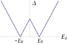
where is the electron spin and is for the K or K’ point (to which we refer also as the K± point). See also the dispersion relation (7) which we derive based on the low-energy effective theory. We emphasize that it is independent of the Rashba SO coupling . The gap (2) vanishes at with
| (3) |
We plot the band gap in the Fig.2.
The gap closes at , where it is a semimetal due to gapless modes. We show the band structure at in Fig.3. It follows from (2) that up-spin () electrons are gapless at the K point (), while down-spin () electrons are gapless at the K’ point (). Namely, spins are perfectly up (down) polarized at the K (K’) point under the uniform electric field .
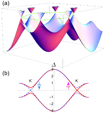
It follows from the gap formula (2) that silicene is an insulator for . In order to tell the difference between the two insulators realized for and , we study the band structure of a silicene nanoribbon with zigzag edges. The gap structure is depicted at two typical points, and , in Fig.4. We see that there are gapless modes coming from the two edges at , as is the demonstration of a topological insulatorLiuPRL . On the other hand, there are no gapless edge modes for , showing that it is a band insulator. We conclude that a topological phase transition occurs between a topological insulator () and a band insulator () as changes.
The reason why gapless modes appear in the edge of a topological insulator is understood as follows. The topological insulator has a nontrivial topological number, the indexKaneMele , which is defined only for a gapped state. When a topological insulator has an edge beyond which the region has the trivial index, the band must close and yield gapless modes in the interface. Otherwise the index cannot change its value across the interface.

III Low-Energy Dirac Theory
We proceed to analyze the physics of electrons near the Fermi energy more in details. The low-energy Dirac theory has been proved to be essential in the study of grapheneSemenoff and its various derivativesBrey73 ; EzawaDirac . It must also be indispensable to explore deeper physics of helical zero modes and promote further researches in silicene.
We may derive the low-energy effective Hamiltonian from the tight binding model (1) around the point asLiuPRB
| (4) |
with
| (5) |
where is the Pauli matrix of the sublattice, m/s is the Fermi velocity, and Å is the lattice constant. It is instructive to write down the Hamiltonian explicitly as
| (6) |
in the basis , where . The two Hamiltonians and are related through the time-reversal operation.
IV Inhomogeneous electric field
The low-energy Dirac theory allows us to investigate analytically the properties of the helical zero mode under inhomogeneous electric field. In so doing we set to simplify calculations. This approximation is justified by the following reasons. First all all, we have numerically checked that the band structure is rather insensitive to based on the tight-binding Hamiltonian (1). Second, appears only in the combination in the Hamiltonian (4), which vanishes exactly at the K± points. Third, the critical electric field is independent of as in (3).
IV.1 Inhomogeneous electric field along -axis
We apply the electric field perpendicularly to a silicene sheet homogeneously in the direction and inhomogeneously in the direction. We may set constant due to the translational invariance along the axis. The momentum is a good quantum number. Setting
| (8) |
we seek the zero-energy solution, where is a four-component amplitude. The particle-hole symmetry guarantees the existence of zero-energy solutions satisfying the relation with . Here, is a two-component amplitude with the up spin and the down spin. Then the eigenvalue problem yields
| (9) |
together with a linear dispersion relation
| (10) |
The equation of motion for reads
| (11) |
We can explicitly solve this as
| (12) |
with
| (13) |
where is the normalization constant. The sign is determined so as to make the wave function finite in the limit . The current is calculated as
| (14) |
This is a reminiscence of the Jackiw-Rebbi modeJakiw proposed for the chiral mode.
The difference between the chiral and helical modes is the presence of the spin factor in the wave function. As we shall see explicitly in some examples in what follows, we find the condition either or for convergence of the wave function. The condition implies that the spin is up () at the K point () and that the spin is down () at the K’ point (). Consequently, the up-spin electrons flow into the positive -direction while the down-spin electrons flow into the negative -direction, implying that the pure spin current flows into the positive -direction. On the other hand, the condition implies that the pure spin current flows into the negative -direction.
Interface between topological and band insulators: We apply an electric field such that
| (15) |
Substituting it to (13), we obtain
| (16) |
where is chosen to make for convergence. The wave function is localized along the two lines taken in the bulk, where the gapless mode emerges since . The currents are helical along these two lines, where along one line and along the other line: The spin currents flow in the opposite directions along these two lines, sandwiched by a band insulator () and a topological insulator (). We illustrate the probability density in Fig.5(a) in the case . Each line may be used as a quantum wire.
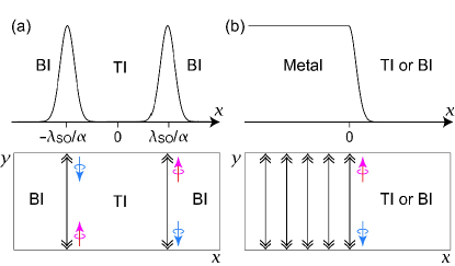
Interface between metal and insulator: We apply an electric field such that
| (17) |
where is the step function: for and for . Substituting it to (13), we obtain
| (18) |
where is chosen to make for convergence. Namely, when we choose , we find
| (19) |
and when we choose , we find
| (20) |
where TI and BI stand for topological and band insulators. In the both cases the region is a metal. Furthermore, it is necessary that for convergence of the wave function, as implies that the current is helical in the metallic region. We illustrate the probability density in Fig.5(b) in the case , which is a constant for .
It is intriguing that there emerge helical zero modes in metal. This is not surprising because the edge of a topological insulator is a sufficient condition but not a necessary condition for the emergence of helical zero modes. The helical zero mode requires the massless Dirac fermion, the time-reversal symmetry and the spin-orbit interaction. Our example shows explicitly that it can appear in regions besides the edge of a topological insulator provided these conditions are satisfied.
IV.2 Inhomogeneous electric field along -axis
We apply a cylindrical symmetric inhomogeneous electric field to a silicene sheet. The equation reads
| (21) |
We solve this for zero-energy states by setting
| (22) |
The equation of motion is transformed into
| (23) |
which we solve as
| (24) |
with
| (25) |
where is the normalization constant and . The sign is determined so as to make the wave function finite in the limit .
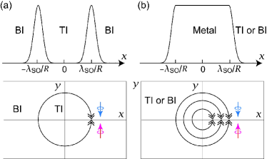
Interface between topological and band insulators: We apply an electric field such that
| (26) |
Substituting it to (25), we have
| (27) |
where is chosen to make for convergence. The wave function is localized along the circle , where . When we choose it is necessary that , and when we choose it is necessary that . In any of the two cases, there emerges helical zero modes and the spin current flows along the circle between a topological insulator () and a band insulator (). The direction of the spin current is opposite for and . We illustrate the probability density in Fig.6(a) in the case . This region may be used as a quantum wire.
Interface between metal and insulator: We apply an electric field such that
| (28) |
where is the step function. Substituting it to (25), we have
| (29) |
where is chosen to make for convergence. It is notable that for and hence the system is metallic there. The wave function describes an interface between a metal for and an insulator for . The insulator is a topological insulator when we choose and a band insulator when we choose . Since it is necessary that for convergence of the wave function, the current is helical in the metallic region (). We show the probability density in Fig.6(b), where constant for . This region may act as a quantum dot.
V Conclusions
Taking advantage of the buckled structure of silicene we have demonstrated that we can control its band structure by applying the electric field . Silicene undergoes a topological phase transition between a topological insulator and a band insulator as crosses the critical point . It is a semimetal at .
A novel phenomenon appears when we apply an inhomogeneous electric field. We have explicitly constructed wave functions of helical zero modes for simple geometrical regions based on the low-energy effective Dirac theory. The results imply in general that helical zero modes can be confined in any regions by tuning the external electric field locally to the critical field (3), . Our system may be the first example in which helical zero modes appear in regions besides the edge of a topological insulator. It is to be emphasized that we can apply an inhomogeneous electric field so that a single silicene sheet contains several regions which are topological insulators, band insulators and metals. Such a structure may open a way for future spintronics. Our results are also applicable to germanene, that is a two-dimensional honeycomb structure made of germanium.
I am very much grateful to N. Nagaosa for many fruitful discussions on the subject. This work was supported in part by Grants-in-Aid for Scientific Research from the Ministry of Education, Science, Sports and Culture No. 22740196.
References
- (1) A.H. Castro Neto, F. Guinea, N.M.R. Peres, K.S. Novoselov and A.K. Geim , Rev. Mod. Phys. 81, 109 (2009).
- (2) M.I. Katsnelson, K.S. Novoselov and A.K. Geim, Nature Physics 2, 620 (2006).
- (3) M. Fujita, K. Wakabayashi, K. Nakada, and K. Kusakabe, J. Phys. Soc. Jpn. 65, 1920 (1996); M. Ezawa, Phys. Rev. B 73, 045432 (2006).
- (4) M. Ezawa, Phys. Rev. B 76, 245415 (2007); J. Fernández-Rossier and J. J. Palacios, Phys. Rev. Lett. 99, 177204 (2007).
- (5) B. Lalmi, H. Oughaddou, H. Enriquez, A. Kara, S. Vizzini, B. Ealet, and B. Aufray, Appl. Phys. Lett. 97, 223109 (2010).
- (6) P.E. Padova, C. Quaresima, C. Ottaviani, P.M. Sheverdyaeva, P. Moras, C. Carbone, D. Topwal, B. Olivieri, A. Kara, H. Oughaddou, B. Aufray, and G.L. Lay, Appl. Phys. Lett. 96, 261905 (2010).
- (7) B. Aufray A. Vizzini, H. Oughaddou, C. Lndri, B. Ealet, and G.L. Lay, Appl. Phys. Lett. 96, 183102 (2010).
- (8) Gian G. Guzmán-Verri and L. C. Lew Yan Voon, Phys. Rev. B 76 (2007) 075131.
- (9) C.-C. Liu, W. Feng, and Y. Yao, Phys. Rev. Lett. 107, 076802 (2011).
- (10) C.-C. Liu, H. Jiang, and Y. Yao, Phys. Rev. B, 84, 195430 (2011).
- (11) M.Z Hasan and C. Kane, Rev. Mod. Phys. 82, 3045 (2010).
- (12) X.-L. Qi and S.-C. Zhang, Rev. Mod. Phys. 83, 1057 (2011).
- (13) C. Wu, B.A. Bernevig and S.-C. Zhang, Phys. Rev. Lett. 96, 106401 (2006).
- (14) C. L. Kane and E. J. Mele, Phys. Rev. Lett. 95, 226801 (2005); ibid 95, 146802 (2005).
- (15) H. Min, J.E. Hill, N.A. Sinitsyn, B.R. Sahu, L. Kleinman, and A.H. MacDonald, Phys. Rev. B 74, 165310 (2006).
- (16) Y. Yao, F. Ye, X.-L. Qi, S.-C. Zhang, and Z. Fang, Phys. Rev. B 75, 041401 (2007).
- (17) J.C. Slonczewski and P.R. Weiss: Phys. Rev. 109, (1958) 272; G.W. Semenoff, Phys. Rev. Lett. 53, 2449 (1984).
- (18) L. Brey and H.A. Fertig, Phys. Rev. B 73, 235411 (2006).
- (19) M. Ezawa, Phy. Rev. B 81, 201402R (2010).
- (20) R. Jackiw and C. Rebbi, Phys. Rev. D 13, 3398 (1976).