Present address: ] i_SW, Arlington, VA 22203, USA.
High mobility two-dimensional hole system on hydrogen-terminated silicon (111) surfaces
Abstract
We have realized a two-dimensional hole system (2DHS), in which the 2DHS is induced at an atomically flat hydrogen-terminated Si(111) surface by a negative gate voltage applied across a vacuum cavity. Hole densities up to cm-2 are obtained, and the peak hole mobility is about cm2/Vs at 70 mK. The quantum Hall effect is observed. Shubnikov-de Haas oscillations show a beating pattern due to the spin-orbit effects, and the inferred zero-field spin splitting can be tuned by the gate voltage.
Metal-oxide-semiconductor (MOS) field-effect transistors (FETs) have long been used to study two-dimensional systems in silicon. While there has been extensive research on two-dimensional electron systems (2DESs) in silicon using MOSFETs over the last several decades,von Klitzing, Dorda, and Pepper (1980); Ando, Fowler, and Stern (1982) comparably little work has been done on two-dimensional hole systems (2DHSs),von Klitzing, Landwehr, and Dorda (1974a, b); Ando, Fowler, and Stern (1982); [][[JETPLett.46; 502(1987)]]Dorozhkin87 primarily due to the fact that holes have lower mobility than electrons, and detailed study was not possible at such low mobility silicon hole devices.
Recently, a new type of silicon FET device has been developed, in which an atomically flat silicon (111) surface is terminated by a monolayer of hydrogen atoms, and a 2DES is induced at the H-Si(111) surface by a positive gate voltage through a vacuum barrier.Eng, McFarland, and Kane (2005) 2DESs in these vacuum FET devices show extremely high mobility.Eng, McFarland, and Kane (2005, 2007); McFarland et al. (2009) In this letter, we report that the vacuum FET technique can be extended to 2DHSs. A peak hole mobility of 104 cm2/Vs is obtained, exceeding by one order of magnitude the mobility in MOS structures and comparable with the mobility of pseudomorphic Si/SiGe heterostructures,Whall et al. (1994); *basaran94; [StrainedGechannelsonSiGevirtualsubstratescanreachahigherholemobilityof$∼$120000cm$^2$/Vsat2K; asshownin][]rossner04 where 2DHSs reside in the SiGe channels. The integer quantum Hall effect (IQHE) is also observed. At lower magnetic fields, Shubnikov-de Haas (SdH) oscillations show a beating pattern, which is due to the zero-field spin splitting.Zawadzki and Pfeffer (2004) In silicon, the spin-orbit effects lift the spin-degeneracy of the heavy hole subband even in a zero external magnetic field. The zero-field spin splitting is from the structure inversion asymmetry (SIA),Winkler (2003) and can be tuned by the external gate. The zero-field spin splitting is of great interest because of its potential use in spintronics devicesDatta and Das (1990) and in studying fundamental physics.Winkler (2003)

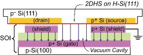
The vacuum FET device includes two pieces, as shown in Fig. 1. One is a p- Si(111) piece (float zone, resistance cm), and the other is a silicon-on-insulator (SOI) piece. First, four p+ contact regions are formed in the Si(111) piece by ion implantation with cm-2, 15 keV boron ions through a 30 nm thick thermal oxide, as shown in the insert of Fig. 2. It is annealed in N2 gas at 1000∘C for 10 minutes to activate dopants and reduce defects. Second, in the SOI piece, the shield and gate conducting layers are formed by double boron ion implantation, and a cloverleaf-shaped cavity is created by dry etching. Finally, the Si(111) piece is H-terminated by immersing it in an ammonium fluoride solution, and then these two pieces are contact bonded in a vacuum chamber. The detailed fabrication processes and the basic operating principle have been discussed elsewhere.Eng, McFarland, and Kane (2005); McFarland (2010) Here the SOI piece acts as a remote gate to induce a 2DHS at the Si(111) surface through the encapsulated vacuum cavity. This cavity also protects the air sensitive H-Si(111) surface. Compared to the Si/SiO2 interface in MOSFETs, the vacuum/H-Si(111) interface is atomically flat and has much fewer defects, leading to a much higher carrier mobility.

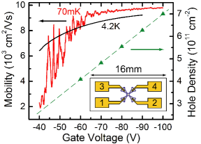
The devices are characterized in a dilution refrigerator with a base temperature of 70 mK. Longitudinal () and Hall () resistances are determined by Van der Pauw measurements with the standard low-frequency AC lock-in technique using a 7 Hz, 100 nA current source. As shown in the insert of Fig. 2, the Van der Pauw geometry consists of a center cloverleaf-shaped 2DHS, which is electric field induced, and four heavily boron-doped contacts (labeled as 1, 2, 3, 4). Four-terminal resistance is defined as , where current is fed from contact i to contact j, and voltage is measured between contacts l and m. The sheet resistance is determined by the standard Van der Pauw technique.van der Pauw (1958) Although the Van der Pauw geometry is symmetric, and are found to differ by 35%, so the sheet resistance, as well as the mobility, is the average of x and y directions.Bierwagen et al. (2004) The anisotropy can be caused by some mechanisms such as miscut, disorder, strain and the non-parabolicity of the valence band,Eng, McFarland, and Kane (2007); McFarland et al. (2009); Ohkawa and Uemura (1975) but the exact sources are yet to be ascertained. Hole density is determined by the magnetic field at the filling factor minimum of the longitudinal resistance curve at T 1 K: , where is the electron charge and is Planck’s constant. The data (triangles) are shown in Fig. 2, and the dashed line is a linear fit. Hole densities up to cm-2 ( V) are obtained. If we use a parallel plate capacitor model, the equivalent depth of the cavity is 759 nm, which is consistent with the measurement result from a profilometer. The extrapolated threshold voltage is V, which indicates the density of the trapped charge at the surface cm-2. The mobility of the 2DHS is also shown in Fig. 2, and the peak mobility is about 9800 cm2/Vs at gate voltage V, T = 70 mK on this device. This is one order of magnitude higher than the hole mobility of a Si(111) MOSFET.von Klitzing, Landwehr, and Dorda (1974b) The contact resistances between the contacts and the 2DHS increase dramatically at V, when the temperature is lowered from 4.2 K to 70 mK. For example, they increase from 20 K to 400 K at V. It is difficult to get reliable measurements at this region, and the calculated mobility shows spurious wild fluctuations at T = 70 mK. Our discussion below will focus on the data at V.

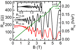
As evidence of the high mobility 2DHS, Fig. 3 shows the longitudinal () and Hall () resistances as a function of perpendicular magnetic field at V ( cm-2) and T = 70 mK. The integer quantum Hall effect (IQHE) is observed. At the vicinity of T, approaches zero, and develops a plateau at . Clear SdH oscillations appear at field above 0.4 T. A close look at the trace of reveals a beating pattern of the SdH oscillations with a node near T, as shown in the insert of Fig. 3. Although the beating pattern has been observed in p-channel Si(110) devices,von Klitzing, Landwehr, and Dorda (1974a); Dorozhkin and Ol’shanetskiǐ (1987) to our best knowledge, this is the first time it has been observed on a Si(111) surface. The beating pattern can be explained by the spin-orbit effects, although different explanations exist. It could be from gross inhomogeneities of the carrier density in the sample.Booth and Ewald (1968) Two samples from different wafers have been measured, and both show a similar beating pattern. At V, the beating node is located at T for the device reported here, and it is at T for the other device. It is therefore highly unlikely that the gross inhomogeneities are the cause.

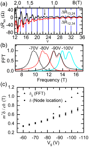
The beating pattern indicates that there are two closely spaced frequency components with similar amplitudes, arising from two populations of holes. The hole subband densities and can be determined by the Fourier analysis of the SdH oscillations with , where is the degeneracy factor, and are the frequencies of the SdH oscillations (Fig. 4(b)).Lu et al. (1998); Winkler et al. (2000) Here vs data in the range T are Fourier transformed after subtraction of a slowly varying background, and peak locations are used as the frequencies of the SdH oscillations. For V (with two well-resolved peaks), must be 1 in order to have the sum of the subband densities equal to the total density, so these two components can only be from one subband with two spin-split levels, i.e. two spin-split subbands.
Landau levels of each spin population give rise to magnetoresistance oscillations with similar amplitude, described by , where is the Fermi energy, is the energy separation between the two spin-split subbands, is , and is the cyclotron frequency.Zawadzki and Pfeffer (2004) The sum of these two components leads to the modulation of the SdH oscillations given by . Beating nodes are located at , etc. Only one node is clearly identified near T (Fig. 3). Fig. 4(a) shows the SdH oscillations in terms of filling factor at V. At , the minima of the SdH oscillations are at the odd numbers of . At , the minima are at the even numbers of . This manifests the transition across the node. We assume that the node corresponds to (highest-field), because the node is most easily observed, and there is no other node up to 6 T.Datta and Das (1990) The node is estimated to be around T, one third of the node, so it is difficult to observe for this device. From the node location , the total spin splitting can be determined by , where is the effective hole mass. In Fig. 4(c), the total spin splitting is described by .
In theories of the spin-orbit interaction, spin splitting can have complicated B dependence.Winkler (2003) The total spin splitting can be expanded as , where is the zero-field spin splitting, is the linear splitting, etc.Zawadzki and Pfeffer (2004) For low magnetic fields, if only the first two terms are considered, then . The frequencies of the SdH oscillations can be used to determined the zero-field spin splitting by . So the zero-field spin splitting can be described by , also shown in Fig. 4(c). There are two important features in the data. First, the zero-field spin splitting increases with increasing perpendicular electric field . Second, at V, , which means that a perpendicular magnetic field can reduce the spin splitting. More detailed analysis is needed to better appreciate the results. These topics will be explored in future studies.
In conclusion, the vacuum FET technique has been demonstrated to create high mobility 2DHSs in Si(111). In these high mobility 2DHSs, we are able to observe the IQHE, and the beating pattern of the SdH oscillations on Si(111) surfaces, which are difficult to reach previously. There are many interesting questions yet to be resolved, such as the non-parabolic valence band structure and the spin-orbit effects. Our high mobility 2DHSs open up new opportunities to explore fundamental physics in the two-dimensional hole systems. In addition, with the ability to create both a 2DES and a 2DHS on a Si(111) surface, it is straightforward to develop a bipolar surface device.
This work was funded by the Laboratory for Physical Sciences. The authors are grateful to Oney Soykal, Charles Tahan, Kevin Eng, and Kei Takashina for insightful discussions and technical help.
References
- von Klitzing, Dorda, and Pepper (1980) K. von Klitzing, G. Dorda, and M. Pepper, Phys. Rev. Lett. 45, 494 (1980).
- Ando, Fowler, and Stern (1982) T. Ando, A. B. Fowler, and F. Stern, Rev. Mod. Phys. 54, 437 (1982), and references therein.
- von Klitzing, Landwehr, and Dorda (1974a) K. von Klitzing, G. Landwehr, and G. Dorda, Solid State Commun. 14, 387 (1974a).
- von Klitzing, Landwehr, and Dorda (1974b) K. von Klitzing, G. Landwehr, and G. Dorda, Solid State Commun. 15, 489 (1974b).
- Dorozhkin and Ol’shanetskiǐ (1987) S. I. Dorozhkin and E. B. Ol’shanetskiǐ, Pis’ma Zh. Eksp. Teor. Fiz. 46, 399 (1987).
- Eng, McFarland, and Kane (2005) K. Eng, R. N. McFarland, and B. E. Kane, Appl. Phys. Lett. 87, 052106 (2005).
- Eng, McFarland, and Kane (2007) K. Eng, R. N. McFarland, and B. E. Kane, Phys. Rev. Lett. 99, 016801 (2007).
- McFarland et al. (2009) R. N. McFarland, T. M. Kott, L. Sun, K. Eng, and B. E. Kane, Phys. Rev. B 80, 161310 (2009).
- Whall et al. (1994) T. E. Whall, A. D. Plews, N. L. Mattey, and E. H. C. Parker, Appl. Phys. Lett. 65, 3362 (1994).
- Basaran et al. (1994) E. Basaran, R. A. Kubiak, T. E. Whall, and E. H. C. Parker, Appl. Phys. Lett. 64, 3470 (1994).
- Rössner et al. (2004) B. Rössner, D. Chrastina, G. Isella, and H. von Känel, Appl. Phys. Lett. 84, 3058 (2004).
- Zawadzki and Pfeffer (2004) W. Zawadzki and P. Pfeffer, Semicond. Sci. Technol. 19, R1 (2004).
- Winkler (2003) R. Winkler, Spin-orbit Coupling Effects in Two-Dimensional Electron and Hole Systems (Springer, Berlin, 2003).
- Datta and Das (1990) S. Datta and B. Das, Appl. Phys. Lett. 56, 665 (1990).
- McFarland (2010) R. N. McFarland, Multi-Valley Physics of Two-Dimensional Electron Systems on Hydrogen-Terminated Silicon (111) Surfaces, PhD dissertation, University of Maryland, Department of Physics (2010).
- van der Pauw (1958) L. T. van der Pauw, Philips Res. Rep. 13, 1 (1958).
- Bierwagen et al. (2004) O. Bierwagen, R. Pomraenke, S. Eilers, and W. T. Masselink, Phys. Rev. B 70, 165307 (2004).
- Ohkawa and Uemura (1975) F. J. Ohkawa and Y. Uemura, Prog. Theor. Phys. Suppl. 57, 164 (1975).
- Booth and Ewald (1968) B. L. Booth and A. W. Ewald, Phys. Rev. 168, 796 (1968).
- Lu et al. (1998) J. P. Lu, J. B. Yau, S. P. Shukla, M. Shayegan, L. Wissinger, U. Rössler, and R. Winkler, Phys. Rev. Lett. 81, 1282 (1998).
- Winkler et al. (2000) R. Winkler, S. J. Papadakis, E. P. De Poortere, and M. Shayegan, Phys. Rev. Lett. 84, 713 (2000).