Planar Superconducting Resonators with Internal Quality Factors above One Million
Abstract
We describe the fabrication and measurement of microwave coplanar waveguide resonators with internal quality factors above at high microwave powers and over at low powers, with the best low power results approaching , corresponding to photon in the resonator. These quality factors are achieved by controllably producing very smooth and clean interfaces between the resonators’ aluminum metallization and the underlying single crystal sapphire substrate. Additionally, we describe a method for analyzing the resonator microwave response, with which we can directly determine the internal quality factor and frequency of a resonator embedded in an imperfect measurement circuit.
High quality factor microwave resonators provide critical elements for superconducting electromagnetic radiation detectors MKID , quantum memories Hofheinz2009 ; Wang2009 , and quantum computer architectures Matteo2011 . Good performance and stability can be achieved for such applications using aluminum resonators patterned on sapphire substrates. Aluminum is a favored material due to its robust oxide and reasonable transition temperature, and sapphire provides an excellent substrate due to its very low microwave loss tangentCreedon2011 and its chemical inertness. However, the quality factors measured in such resonators is lower than expected; recent simulations Wenner2011 and experiments Wisbey2010 suggest that the unexplained loss arises mostly from imperfections at the metal-substrate interface. Using an experimental apparatus with minimal stray magnetic fields and infrared light at the sample Barends2011 , here we show that careful substrate preparation and cleaning yields aluminum-on-sapphire resonators with significantly higher internal quality factors . We also introduce a new method for evaluating the resonator microwave response.
The aluminum for the resonators was deposited on c-plane sapphire substrates in one of three deposition systems: A high vacuum DC sputter system (base pressure Torr), a high vacuum electron-beam evaporator ( Torr) or an ultra-high vacuum (UHV) molecular beam epitaxy (MBE) system ( Torr) with electron-beam deposition. The sapphire substrates were first sonicated in a bath of acetone then isopropanol followed by a deionized water rinse. For the sputter-deposited and e-beam evaporated samples, we further cleaned the substrates prior to Al deposition by Ar ion-milling. For the MBE-deposited samples, we first cleaned the substrates with a load-lock outgassing at 200∘C followed by heating to 850∘C, in UHV or in Torr of activated oxygen (O) generated from a radio-frequency plasma source. After substrate treatment, 100 nm of Al was deposited at room temperature. Specific process parameters are given in Table 1.
| Process111All films deposited at room temperature. | In vacuo | -H | -L | ||
| cleaning | (m) | (GHz) | |||
| A) Sputter | 100 eV Ar+ mill | 3 | 3.833 | ||
| for 2 min | 15 | 6.129 | |||
| B) E-beam | 60 eV Ar+ mill | 3 | 3.810 | ||
| for 10 sec | 15 | 6.089 | |||
| C) MBE | None | 6 | 4.973 | ||
| 15 | 6.120 | ||||
| D) MBE | LL222200∘C anneal in load lock ( Torr). anneal | 3 | 3.773 | ||
| 15 | 6.125 | ||||
| E) MBE | LL222200∘C anneal in load lock ( Torr). & 850∘C anneal | 3 | 3.876 | ||
| 15 | 6.127 | ||||
| F) MBE | LL222200∘C anneal in load lock ( Torr). & 850∘C anneal | 3 | 3.767 | ||
| in O 333Activated oxygen (O) generated from a radio frequency plasma source. | 15 | 6.121 | |||
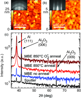
The substrate cleaning process changes the morphology of the deposited Al film, as shown in Fig. 1: No cleaning yields a rough Al film and a diffuse polycrystalline reflected high-energy electron diffraction (RHEED) pattern, while a high-temperature anneal gives a much smoother film and sharp crystalline RHEED. X-ray diffraction scans of all films show strong sapphire substrate peaks as well as an Al(111) peak [Fig. 1(c)], with the MBE-grown samples displaying stronger Al peaks. MBE-grown samples heated to 850∘C with or without O, and MBE samples that underwent only a 200∘C anneal (not shown), had RHEED, atomic-force microscopy, and x-ray diffraction scans that were nearly indistinguishable from one another.

We patterned resonators from the Al films using an optically-patterned resist and etching in a 300 W BCl3/Cl2 inductively-coupled plasma. This step defined sets of 12 quarter-wave coplanar waveguide resonators capacitively-coupled to a single central transmission line Barends2011 . Resonators were designed with one of three center trace widths: = 3 m, 6 m or 15 m. The center trace gap to the ground planes on either side was . The resonator coupling to the central transmission line corresponded to one of the coupling strengths Mazinthesis = , , or ; resonator frequencies ranged from 4 to 8 GHz.
After etching, we stripped the resist and diamond saw-cut the wafers into mm2 dies, placing individual dies in an Al sample box and wiring with 25 m dia. Al wire-bonds. We mounted the sample box on the 50 mK stage of an adiabatic demagnetization refrigerator, enclosed in a copper light-tight shield, surrounded by a magnetic shield at 4 K, as described in Ref. Barends2011, . We note that all screws and coaxial connectors were made of non-magnetic materials. The use of non-magnetic materials inside of the 4 K magnetic shield reduced the residual magnetic field at the sample from 100 mG to 3 mG, which we verified using cryogenic tests similar to Ref. Wang2009, .
We measured the transmission coefficient of the 50 mK resonators with a vector network analyzer (VNA). The cryostat microwave input cable had 40 dB attenuation at room temperature and 30 dB attenuation at the 4 K stage, followed by 50 mK microwave powder filters Barends2011 with 1 dB attenuation before the connection to the sample’s central transmission line. The sample’s output passed through a second 50 mK microwave powder filter followed by a circulator at 4 K, which protects the resonators from noise originating in the high electron mobility transistor (HEMT) amplifier (noise temperature 4.5 K) also located at 4 K.
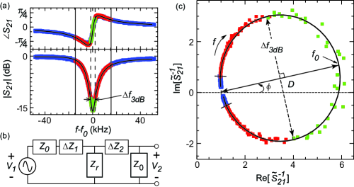
A typical normalized transmission spectrum is shown in Fig. 2(a), displaying a dip in and a step in the phase of near the resonance frequency . Note the slight asymmetry about in both the magnitude and phase, which we attribute to a small impedance mismatch in the central transmission line on either side of the resonatorKhalil2011 , likely originating from the wire-bond connections wirebonds , sample mount imperfections, or the transmission line geometry. Analyzing a circuit that includes small in-line complex impedances and on either side of the resonator [Fig. 2(b)], the transmission is given by
| (1) |
where is the cable impedance, , , , and the impedance of the resonator in series with its coupling capacitor is given by Mazinthesis , for frequencies near resonance,
| (2) |
with , and are the internal and coupling quality factors, respectively. The nearly frequency-independent pre-factor in Eq. (1), of order unity, is absorbed in an off-resonance transmission calibration of the cabling and amplifiers, leaving us with a normalized inverse transmission given by
| (3) |
with the magnitude of absorbed in the re-scaled coupling quality factor .

In Fig. 2(c) we display the data in Fig. 2(a) in the inverse transmission complex plane. In this representation the resonator response is a circle starting and ending at , achieved for frequencies far from resonance. At resonance , is diametrically opposite , with diameter and the circle center rotated from the real axis by the impedance mismatch angle . The two frequency points around the circle from the resonance frequency are the 3 dB points, with their frequency difference the full width at half maximum (FWHM) of , yielding the internal quality factor . Eq. (3) and the plot of Fig. 2(c) not only allow the internal quality factor to be determined directly, these also emphasize how to properly measure and visually scrutinize the data.
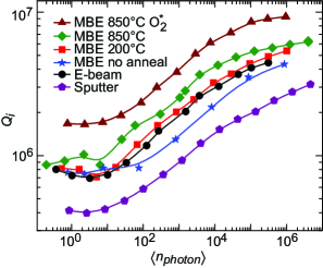
The low-power ’s of 15 m center trace width resonators [Fig. 3] range from for the sputtered film with ion mill substrate cleaning to for the MBE-deposited resonator shown in Fig. 2. We find that as the measurement microwave power is increased [Fig. 3], the internal quality factors remain roughly proportional, with for most resonators increasing by about a factor of ten between high and low powers. The increase in with power is consistent with loss being dominated by interfacial and surface two-level-states (TLS)Wenner2011 ; Sage2011 .
We discovered that for the highest quality factor resonators at the lowest powers, the internal quality factor can fluctuate in time by as much as 30% over a period of several hours, a variation significantly larger than the statistical uncertainty of the fit . We believe this is due to fluctuations in the population of TLS, which we are actively studying. The values for reported in this Letter are long-term averages rather than the highest transient values, and are representative of many different samples.
Most significantly, we see a systematic dependence of on the substrate cleaning and deposition process. We attribute this dependence to changes in the Al-sapphire interface, in agreement with simulations Wenner2011 . The sputtered film resonators had the lowest for all powers, and are comparable to the published literature Wang2009 ; Sage2011 ; Khalil2011 . We believe the lower measured here is due to the pre-deposition ion mill, which may remove most surface contaminants, but may also bury some contaminants as well as leave a damaged substrate surface Day1993 . The ion mill used for e-beam evaporation was lower in energy and duration than that for the sputtered films, and produced resonators with ’s comparable to those deposited by MBE with no substrate anneal.
We obtained better resonator quality factors with MBE-grown Al with pre-deposition annealing, consistent with better surface properties as shown by RHEED and AFM [Fig. 1]. However, the very best quality factors were achieved with high temperature (850∘C) anneals in O, yielding significantly higher even though RHEED and AFM are nearly identical to other MBE-annealed samples. These results are consistent with microscopic theories attributing TLS to surface-bound hydroxyl groups Phillips1987 , which can saturate the sapphire (0001) surface Rabalais1997 , and remain even after annealing at 1100∘C in UHV Rabalais1997 ; Niu2000 . Carbon and hydrogen have also been observed on sapphire after similar annealing processes Niu2000 . The highly reactive activated oxygen used here may remove such surface-bound molecules, more effectively than a simple anneal, and with less damage than with ion milling, although we cannot at present verify these hypotheses.

In summary, we have measured the internal quality factors of superconducting aluminum resonators while varying the substrate preparation, deposition method and measurement power. Cleaning the substrate surface as thoroughly as possible without damaging the underlying crystal leads to the highest at single photon energies, achieved for resonators with m and GHz. The same process also produces the best high-power , but for resonators with m and GHz.
The authors thank B. A. Mazin for stimulating discussions. Devices were fabricated at the UCSB Nanofabrication Facility, a part of the NSF-funded National Nanotechnology Infrastructure Network. M. M. acknowledges support from an Elings Postdoctoral Fellowship. This work was supported by IARPA under ARO award W911NF-09-1-0375.
References
- (1) P. K. Day, H. G. LeDuc, B. A. Mazin, A. Vayonakis, and J. Zmuidzinas, Nature (London) 425, 817 (2003).
- (2) M. Hofheinz, H. Wang, M. Ansmann, R. C. Bialczak, E. Lucero, M. Neeley, A. D. O’Connell, D. Sank, J. Wenner, J. M. Martinis, A. N. Cleland, Nature (London) 459, 546-549 (2009).
- (3) H. Wang, M. Hofheinz, J. Wenner, M. Ansmann, R. C. Bialczak, M. Lenander, E. Lucero, M. Neeley, A. D. O’Connell, D. Sank, M. Weides, A. N. Cleland, and J. M. Martinis, Appl. Phys. Lett. 95, 233508 (2009).
- (4) M. Mariantoni, H. Wang, T. Yamamoto, M. Neeley, R. C. Bialczak, Y. Chen, M. Lenander, E. Lucero, A. D. O’Connell, D. Sank, M. Weides, J. Wenner, Y. Yin, J. Zhao, A. N. Korotkov, A. N. Cleland, J. M. Martinis, Science 334, 61 (2011).
- (5) D. L. Creedon, Y. Reshitnyk, W. Farr, J. M. Martinis, T. L. Duty, M. E. Tobar, Appl. Phys. Lett. 98, 222903 (2011).
- (6) J. Wenner, R. Barends, R. C. Bialczak, Y. Chen, J. Kelly, E. Lucero, M. Mariantoni, A. Megrant, P. J. J. O’Malley, D. Sank, A. Vainsencher, H. Wang, T. C. White, Y. Yin, J. Zhao, A. N. Cleland, and J. M. Martinis, Appl. Phys. Lett. 99, 113513 (2011).
- (7) D. S. Wisbey, J. Gao, M. R. Vissers, F. C. S. da Silva, J. S. Kline, L. Vale, and D. P. Pappas, J. Appl. Phys. 108, 093918 (2010).
- (8) R. Barends, J. Wenner, M. Lenander, Y. Chen, R. C. Bialczak, J. Kelly, E. Lucero, P. J. J. O’Malley, M. Mariantoni, D. Sank, H. Wang, T. C. White, Y. Yin, J. Zhao, A. N. Cleland, J. M. Martinis, and J. J. A. Baselmans, Appl. Phys. Lett. 99, 113507 (2011).
- (9) B. A. Mazin, Ph.D. thesis, California Institute of Technology, 2004.
- (10) M. S. Khalil, F. C. Wellstood, K. D. Osborn, IEEE Transactions on Applied Superconductivity 21, 879 (2011).
- (11) G. J. Grabovskij, L. J. Swenson, O. Buisson, C. Hoffmann, A. Monfardini, and J.-C. Villégier, Appl. Phys. Lett. 93, 134102 (2008).
- (12) J. M. Sage, V. Bolkhovsky, W. D. Oliver, B. Turek, and P. B. Welander, J. Appl. Phys. 109, 063915 (2011).
- (13) M. E. Day, M. Delfino, W. Tsai, A. Bivas, and K. N. Ritz, J. Appl. Phys. 74, 5217 (1993).
- (14) W. A. Phillips, Rep. Prog. Phys. 50, 1657 (1987).
- (15) J. Ahn, J. W. Rabalais, Surf. Sci. 388, 121 (1997).
- (16) C. Niu, K. Shepherd, D. Martini, J. Tong, J. A. Kelber, D. R. Jennison, and A. Bogicevic, Surf. Sci. 465, 163 (2000).