Conductance of a STM contact on the surface of a thin film
Abstract
The conductance of a contact, having a radius smaller than the Fermi wave length, on the surface of a thin metal film is investigated theoretically. It is shown that quantization of the electron energy spectrum in the film leads to a step-like dependence of differential conductance as a function of applied bias . The distance between neighboring steps in equals the energy level spacing due to size quantization. We demonstrate that a study of for both signs of the voltage maps the spectrum of energy levels above and below Fermi surface in scanning tunneling experiments.
pacs:
74.55.+v, 85.30.Hi, 73.50.-hI Introduction
Today a fairly large number of papers have addressed the problem of calculating point-contact conductance for use in analyzing and interpreting scanning tunneling microscopy (STM) experiments (for reviews see, for example, Hofer ; Blanco ). The low symmetry of the problem and the wide variety of objects under study do not allow developing a general theory of STM, and different approaches for specific problems are used. The theory papers on this subject can be divided into two groups: One uses methods taking into account the specific atomic structure of the STM tip and that of the test specimen. These methods make it possible to reproduce the crystallographic structure of the sample surface in the calculated STM images and this is very useful for arriving at a correct interpretation of experimental data. The main deficiency of this approach is the lack of analytical formulas for the STM current-voltage characteristics as numerical calculations must be performed for every specific case. The other group of works exploit simplified models of noninteracting electrons which allows finding relatively simple analytical expressions that describe the STM current qualitatively. For this reason such theoretical results are widely used by experimentalists.
One of the first free-electron models describing STM experiments was proposed by Tersoff and Hamann Tersoff whose theoretical analysis of tunnel current is based on Bardeen’s formalism Bardeen , in which a tunneling matrix element is expressed by means of independent wave functions for the tip and the sample within the barrier region. Using the model wave functions the authors Tersoff showed that the conductance of the system is proportional to the local density of states of the sample at the tip position. In principle it is possible to extract information on subsurface objects (single defects, clusters, interfaces etc.) by STM, but this requires a more detailed theoretical analysis Kobayashi , which takes into account the influence of subsurface electron scattering on the tunneling current.
The physical picture of an electron tunneling through a classically forbidden region is that the electron flow emerging from the barrier is defined by the matching of the wave functions of carriers incident on the barrier and those that are transmitted. For a three dimensional STM geometry the wave functions for electrons transmitted through the vacuum region radically differs from the electron wave functions in an isolated sample and they describe the electron propagation into the bulk from a small region on the surface below the STM tip. In contrast, the theory of Ref. Tersoff and its modifications (see Hofer ; Blanco and references therein) uses unperturbed wave functions of the surface Bloch states. Changes in the wave functions of transmitted electrons due to scattering by subsurface objects provide the information about such scattering in the STM conductance.
In Ref. Avotina2005 it was proposed to introduce in the theory of STM the model by Kulik et al. Kulik . In this model a three dimensional STM tip is replaced by an inhomogeneous barrier in an otherwise nonconducting interface that separates the two conductors. In Ref. Kulik it was shown that under assumption of small transparency of the tunnel barrier the wave function (and thus the current-voltage characteristics) can be found analytically for an arbitrary size of the tunnel area. The results in Avotina2005 for the conductance of the tunnel point-contact were generalized to an arbitrary Fermi surface for the charge carriers in Ref. Avotina06 . In a series of papers the model Kulik has been expanded to describe oscillations of the STM conductance resulting from electron scattering by subsurface defects (for reviews see AKR ; Khotkevych ).
Scanning tunneling microscopes have been widely used for the study of various small-sized objects: islands, thin films deposited on bulk substrates, etc Altfeder1997 -Gasparov . First, a discrete periodic spatial variation of the STM current originating from the quantization of electron states was observed in the quantum wedge: a nanoscale flat-top Pb island on a stepped Si(111) surface Altfeder1997 . Later these authors showed that that the lattice structure of an interface buried under a film of Pb, whose thickness can be as many as 10 times the Fermi wavelength, can be clearly imaged with STM Alt2 . They concluded that the key to the transparency of a metal lies in a highly anisotropic motion of the electrons and the strong quantization of their transverse wave function components. In the paper Jiang the electronic states of thin Ag films grown on GaAs(110) surfaces was investigated by STM with single-layer thickness resolution, and the quantum-well states arising from the confinement geometry of the Ag films have been identified. Quantum size effects, manifested in the formation of new electronic bound states, were investigated by STM on thin Pb islands of varying heights on the Si(111)-(77) surface in Ref.Su . In experiments Alt it was demonstrated that scanning tunneling microscopy and spectroscopy of epitaxial Pb islands on Si(111) reveal adiabatic lateral modulation of the energy spectra of the quantum well, providing remote electronic images of the subsurface reflection phase. In Ref. Hongbin a step structure at the buried Pb on Si(111) 66-Au interface was determined by utilizing the presence of quantum well states. It was demonstrated that the spatial step positions as well as the step heights can be extracted nondestructively and with atomic layer precision by STM. Vertical Friedel oscillations in interface-induced surface charge modulations of Pb islands of a few atomic layers on the incommensurate Si(111)-Pb surface have been observed Jian . Thus, detailed experimental results have been obtained, but a microscopic theory for STM tunneling spectra on samples of finite size has not been reported, which provides the motivation for the present work. Current-voltage characteristics for size quantization in planar thin film geometries of metal-insulator-metal tunneling junctions have been investigated theoretically in Refs. Davis1 ; Khachaturov . Standing electron wave states in thin Pb films have been observed by electron tunneling in early experiments by Lutskii et al. Lutskii .
In this paper we present the differential conductance for small contacts, having a radius smaller than the Fermi wave length where is the Fermi momentum. The contacts are formed on the surface of a thin metal film and we analyze the voltage dependence of and . We focus on the size quantization effects of the electron energy spectrum in the film on .
The organization of this paper is as follows. The model that we use to describe the contact, and the method for obtaining a solution of the three-dimensional Schrödinger equation asymptotic in the small radius of the contact, are described in Sec. II. In Sec. III the current-voltage characteristics and the differential conductance are found on the basis of a calculation of the probability current density through the contact. Sec. IV presents a physical interpretation of the results obtained. In Sec. V we conclude by discussing the possibilities for exploiting these theoretical results for interpretation of electron energy spectroscopy in thin films by STM. In the appendixes we solve the Schrödinger equation for the tunnel point contact in framework of our model (App.I) and for a point contact without barrier (App.II) and find the wave functions for electrons transmitted through the contact. These solutions are used in Sec.III for the calculation of current.
II Model and electron wave function of the system
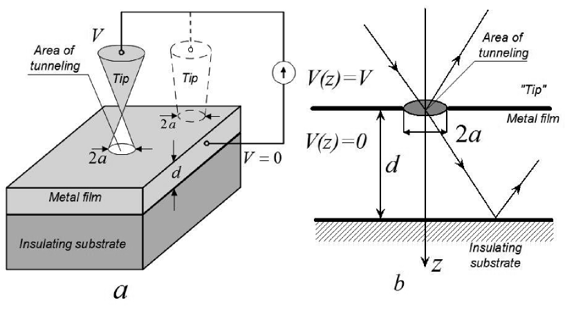
The model that we consider is illustrated in Fig. 1. Electrons can tunnel through an orifice centered at the point in an infinitely thin insulating interface at from a conducting half-space (the tip) into a conducting sheet of thickness (Fig.1(b)). The radius of the contact and the thickness of the film are assumed to be much smaller than the shortest mean free path, i.e we consider a purely ballistic problem.
The wave function satisfies the Schrödinger equation
| (1) |
In Eq.(1) and are electron effective mass and energy, respectively. The inhomogeneous potential barrier in the plane we describe by the function , where is a two dimensional position vector in the plane and , with the Heaviside step function. For such model the wave function satisfies the following boundary conditions at the interface and at the metal sheet surface
| (2) |
| (3) |
| (4) |
Eqs. (1)-(4) can be solved in the limit of a small contact, ( is the absolute value of the electron wave vector ). In the zeroth approximation in the contact diameter the solutions of Eq.(1) for are independent and satisfy the zero boundary condition at the impenetrable interface at The quantum states in the conducting half-space (the tip) are defined by the three components of the electron wave vector , with a two-dimensional vector parallel to the interface. In the metal film the quantum states are characterized by a two-dimensional vector perpendicular to the axis and by the discrete quantum number which results from the finite size of the conductor in the direction. The energy eigenvalues and eigenfunctions for the two disconnected conductors are given by
| (5) | |||
| (6) |
and
| (7) | |||||
| (8) |
where In Eqs. (6) and (8) we use a wave function normalization with unit amplitude of the wave incident to the interface.
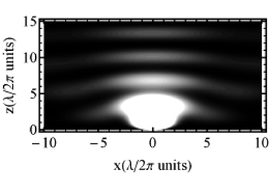
The partial wave for the first order approximation in the small parameter , which describes the transition of electrons from one to the other conductor, is given in the appendices. Appendix I, Eqs. (AI.5) and (AI.6), gives the solution for a tunnel point contact, having a potential barrier of small transparency at the orifice in the plane . Appendix II, Eqs. (AII.6) - (AII.8), gives the solutions for a contact without barrier. Figure 2 illustrates the spacial variation of the square modulus of the wave function for electrons transmitted through the contact into the film.
III Current-voltage characteristic and conductance of a point contact.
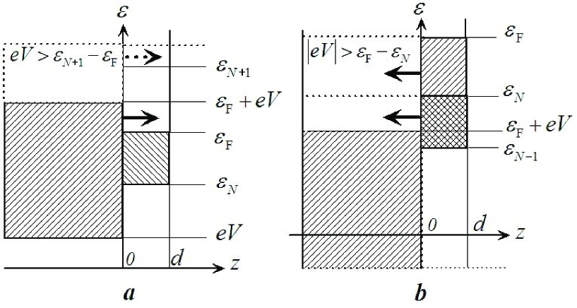
As has been shown in Ref. KOSh for a ballistic point contact of small radius with much smaller than the electron mean free path , the electrical potential drops over a distance from the contact, and in the limit the potential can be approximated by a step function . In this approximation, for the calculation of the electrical current we can take the electron distribution functions at as the Fermi functions with energies shifted by the applied bias ( is the negative electron charge), Figure 3 illustrates the occupied energy states in the two conductors for both signs of the applied bias . At the electrons flow from the bulk conductor (the tip) into the film and, vice-versa, at they flow from the film into the massive conductor.
The total current through the area of the contact can be found by integration over the flux in both directions
| (9) | |||
In Eq. (9) we integrate over the wave vector in the semi-infinite conductor for the current in the negative direction (first term), and integrate over the two-dimensional wave vector and sum over the discrete quantum number for the opposite direction of the current (second term).
For simplicity we will take the temperature to be zero. In this case the electric current is defined by electrons passing the contact in one direction only, depending on the sign of the applied bias. The flux integrated over the area of the contact is calculated in the usual way
| (10) |
where The wave function should be taken as the wave transmitted through the contact, given by equations (AI.5) and (AII.6) with for electron flux from the tip to the sheet, , and by equations (AI.6) and (AII.7) with for fluxes in the opposite direction. The energy shift in the region should be taken into account, which for our choice of the reference point of energy (see Fig. 3) implies that the absolute value of the electron wave vector in the half-space is given by
For the tunnel point contact (tpc) the flux can be expressed in terms of the wave function in the contact plane (AI.1), and we obtain,
| (11) |
and
| (12) |
Here, is the angle between the vector and the axis, and with the integer part of
For a metallic point contact (mpc) without barrier the expressions for the flux are written by means of Eqs. (AII.4), (AII.9)-(AII.11),
| (13) |
and
| (14) |
Substituting Eqs. (11)-(14) into the general expression (9) we find the current-voltage characteristic of the system
| (15) |
and
| (16) | |||
where is the Fermi energy,
| (17) |
| (18) |
is a finite sum of powers of integer numbers,
| (19) |
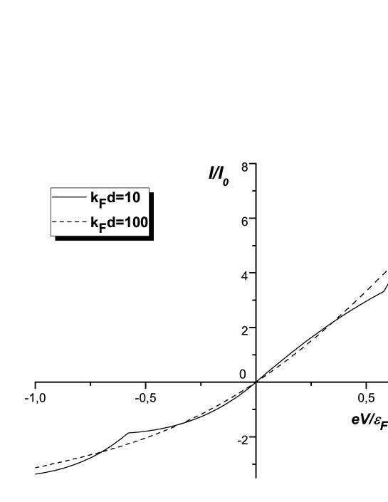
Note that where are generalized harmonic numbers. The current is plotted in Fig. 4 as a function of bias voltage for two choices of the film thickness.
Differentiating Eqs. (15) and (16) with respect to voltage we obtain the differential conductance for a point contact with radius ,
| (20) |
| (21) | |||
In the limit the zero-bias conductance taken from both sides coincides, as it should,
| (22) |
where , and is the conductance of the contact between the bulk conductor (the tip) and a thin film that has only a single energy level available below for the motion along ,
| (23) |
is the conductance of a contact between two conducting unbound half-spaces. For a tunnel point contact this is given by Kulik ; AKR
| (24) |
and for a metallic point contact we have ISh ,
| (25) |
For Eqs. (20) and (21) transform into the known voltage dependence of the conductance for a point contact between unbound conducting half-spaces Avotina08mi ,
| (26) |
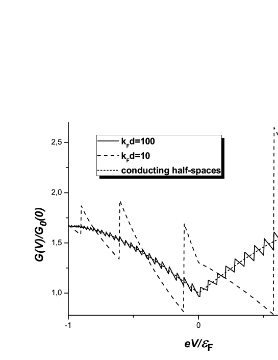
IV Discussion
Thus, in the framework of the model illustrated in Fig. 1 we have obtained the current-voltage characteristic and the differential conductance for a contact on the surface of a thin metal film. Under the assumption that the contact radius is much smaller than the Fermi wave length we found asymptotically exact formulas for the dependence of the total current (Eqs. (15) and (16)) and the contact conductance (Eqs. (20), (21)) on the applied voltage. In the limit of zero temperature and neglecting scattering processes we have demonstrated that the dependence has kinks and undergoes jumps at the same values of applied bias (see Fig.4 and Fig.5) These events result from the size quantization of the electron spectrum in the film.
The results obtained show that even in Ohm’s-law approximation (22), , the conductance is not simply proportional to the electron density of states (DOS) in the isolated film,
| (27) |
It is remarkable that the dependence of the conductance (22) on the number of quantum levels is the same for, both, tunnel and metallic point contacts. This fact shows that such dependence is not sensitive to the model taken for the potential barrier, and that it is the result of the point-contact geometry. Recently, the relationship between the differential conductance and the local density of states has been studied in a tight-binding approximation for tunnel junctions, where the junction geometry can be varied between the limiting cases of a point-contact and a planar junction Berthod . In the framework of a real-space Keldysh formalism the authors of Ref. Berthod have shown that the differential conductance is not, in general, proportional to the sample DOS for planar junctions, although features of the DOS may be present.
From Eqs. (20) and (21) it follows that the the conductance is non-symmetric in the applied bias. This asymmetry can be explained as follows: Let and electrons tunnel from the bulk conductor into the film (Fig. 3a) in which subbands of the size quantization are partially filled. If the bias is smaller than the distance between the Fermi level and the bottom of the next (empty) subband the electron can tunnel into any of the subbands. At tunneling into the -th subband becomes possible and the conductance undergoes a positive jump. Such jumps are repeated for increasing voltage for all higher subbands. For when electrons tunnel from the thin film into bulk metal (Fig. 3b) the situation is somewhat different. If the bias becomes larger than distance between the bottom of the last partially filled subband and Fermi energy, , the contribution of the -th subband to the tunnel current does not depend on the voltage because for any all electrons of this subband can tunnel into the bulk states of the left conductor. For this reason the differential conductance drops for values of coinciding with bottoms of subbands of size quantization in the film. The distance between neighboring jumps of the conductance on the voltage scale equals the distance between energy levels For the number of conductance jumps is finite and equals the number of discrete levels below Fermi surface The asymmetry around and the general shape of the jumps in the conductance can be recognized in the experiments, see e.g. Jiang . In the special case of a 2D electron system, which has only one level in the potential well, there is a single negative jump of Such a jump has been observed in Ref. Burgi by STM investigations of the 2D electron gas at noble-metal surfaces. For the number of conductance jumps formally is not restricted. However, for our approach is no longer applicable and the influence of field emission on the tunnel current must be taken into account Kempen ; Mongenstern
The observation of manifestations of the size quantization in the STM conductance requires a few conditions which must be fulfilled: The distance between the energy levels must be large enough and should satisfy the condition where is the mean scattering time of the electrons in the film and is the temperature. The surfaces of the metal film in the region of the contact must be atomically smooth Tavger . When a finite lifetime of the quantized states becomes relevant, the temperature broadening of the Fermi function, or surface imperfections need to be taken into account this will result in a rounding of the jumps in the curve presented in Fig. 5 (Eqs.20, 21), which was plotted under assumptions of perfectly specular surfaces, and With these restrictions taken into account the current-voltage curves in Fig. 4 give a fair qualitative description of the experimental results of Ref. Alt2 .
It can be easily seen that the results obtained have a more wide domain of applicability than that of a rectangular well for the conducting film. For any model of the potential which restricts the electron motion in one direction the differential conductance has a step-like dependence on the applied bias with distances between the steps equal to the distances between the quantum levels.
V Conclusion.
In summary, we have investigated the conductance of ultra small contacts, for which the radius is smaller than the Fermi wave length, on top of the surface of a thin film. The discreteness of the component of the electron momentum transverse to the film surface is taken into account, where the distance between the electron energy levels due to the size quantization is assumed to be larger than the temperature. Both, a contact with a potential barrier of low transparency, and a contact without barrier have been considered. In framework of our model, using a -function potential barrier, the current-voltage characteristic of the system and differential conductance have been obtained. We predict a sawtooth dependence of on the applied bias and show that the distance between neighboring jumps is equal to the distance between neighboring energy levels of size quantization, i.e. this dependence can be used for spectroscopy of size quantization levels. At the jumps in the conductance are positive and correspond to distances between levels above the Fermi surface, while undergoes negative jumps for , the distances between which are equal to the distances between the levels below the Fermi surface. The predicted quantization of the conductance can be observed in STS experiments, and the shape of the theoretical curves agrees well with experiments.
VI Appendix I: Electron tunneling between the tip and the thin film.
We search a solution to Eq. (1) at in the form of a sum for the incident and backscattered waves, and for the transmitted wave. Here, , as given by Eqs. (6), (8), is the unperturbed wave function that does not depend on the barrier amplitude , while gives the first order correction. Substituting the wave function into the boundary conditions (2) and (3) one should match terms of the same order in As a result the boundary condition (3) becomes Kulik
| (AI.1) |
where when the wave is incident to the contact from the tip side, and when the wave arrives at the contact from the sheet. For we have in the plane of the contact and we can neglect the exponent in the boundary condition (AI.1).
The function can be represented as a Fourier integral
| (AI.2) |
The Fourier components in (AI.2) should satisfy the zero boundary condition at , but are otherwise freely propagating along ,
| (AI.3) |
| (AI.4) |
with From Eqs. (AI.1), (AI.2) it follows that
| (AI.4) |
Substituting this into Eq. (AI.2) we find the wave functions for the electrons transmitted through the contact as,
| (AI.5) |
| (AI.6) |
where is the Bessel function of the first kind.
VII Appendix II: metallic point contact between STM tip and metal film.
Here we consider a point contact without potential barrier in the plane of the interface. When the contact radius is small, , we can use perturbation theory for the electron wave function in the limit In zeroth approximation the wave functions are given by Eqs. (6) and (8). The first order correction, , to the wave function in the plane of the contact can be found by the method proposed in ISh . For distances from the contact we can neglect the second term in the Schrödinger equation (1) and it reduces to the Laplace equation. We express the wave function in coordinates of an oblate ellipsoid of revolution , with and . As a consequence of the cylindrical symmetry of the problem the wave function does not depend on The interface corresponds to and the plane of the orifice is at In these coordinates we obtain the equation
| (AII.1) |
with the boundary condition at the interface
| (AII.2) |
The solution of the boundary problem (AII.1), (AII.2) is
| (AII.3) |
where and are constants. For Eq. (AII.3) gives the function in the plane of the contact
| (AII.4) |
As in Appendix I, we express as a Fourier integral and, using the Eq. (AII.4), we find for the Fourier components,
| (AII.5) |
where is the spherical Bessel function of the first kind. Substituting Eq. (AII.5) into Eq. (AI.2) and using Eqs. (AI.3), (AI.4) we obtain
| (AII.6) |
and
| (AII.7) |
The constant must be found from the boundary condition (3) at , which for this case takes the form
| (AII.8) |
The meaning of the symbol is explained below Eq.(AI.1). Differentiating Eqs. (AII.6) and (AII.7) with respect to and calculating the integrals in the limit of small we find,
| (AII.9) |
| (AII.10) |
where with the integer part of Substituting Eqs. (AII.9) and (AII.10) into (AII.8) in leading approximation in in which only first terms in brackets (proportional to ) should be taken into account, we find for the unknown constant,
| (AII.11) |
References
- (1) W. A. Hofer, A. S. Foster, A. L. Shluger, Rev. Mod. Phys., 75, 1287 (2003).
- (2) J. M. Blanco, F. Flores, Rubén Pérez, Progr. Surface Science, 81, 403 (2006).
- (3) J. Tersoff, D. Hamann, Phys. Rev. Lett. 50 1998 (1983); Phys. Rev. B, 31, 805 (1985).
- (4) J. Bardeen, Phys. Rev. Lett. 6, 57 (1961).
- (5) K. Kobayashi, Phys. Rev. B, 53, 11091 (1996).
- (6) Ye.S. Avotina, Yu.A. Kolesnichenko, A.N. Omelyanchouk, A.F. Otte, and J.M. van Ruitenbeek, Phys. Rev. B 71, 115430 (2005).
- (7) I.O. Kulik, Yu.N. Mitsai, A.N. Omelyanchouk, Zh. Eksp. Theor. Phys. 63, 1051 (1974).
- (8) Ye. S. Avotina, Yu. A. Kolesnichenko, A.F. Otte, and J.M. Ruitenbeek, Phys. Rev. B, 74, 085411 (2006).
- (9) Ye. S. Avotina, Yu. A. Kolesnichenko and J. M. van Ruitenbeek, Low Temp. Phys., 36, 849 (2010) [Fiz. Nizk. Temp., 36, 1066 (2010)].
- (10) N. V. Khotkevych , Yu. A. Kolesnichenko and J. M. van Ruitenbeek, Low Temp. Phys. 37, 53 (2011) [Fiz. Nizk. Temp., 37, 64 (2011)]
- (11) I. B. Altfeder, K. A. Matveev, and D. M. Chen, Phys. Rev. Lett. 78, 2815 (1997).
- (12) I. B. Altfeder, D. M. Chen, and K. A. Matveev, Phys. Rev. Lett. 80, 4895 (1998).
- (13) C.-S. Jiang, H.-B. Yu, X.-D. Wang, C.-K. Shih, and Ph. Ebert, Phys. Rev. B 64, 235410 (2001).
- (14) W. B. Su, S. H. Chang, W. B. Jian, C. S. Chang, L. J. Chen, and Tien T. Tsong, Rev. Lett. 86 5116 (2001).
- (15) I. B. Altfeder, V. Narayanamurti, and D. M. Chen, Phys. Rev. Lett. 88, 206801 (2002).
- (16) Hongbin Yu, C.-S. Jiang, Ph. Ebert and C.-K. Shih, Appl. Phys. Lett., 81, 2005 (2002).
- (17) W. B. Jian, W. B. Su, C. S. Chang, and T.T. Tsong, Phys. Rev. Lett. 90 196603 (2003).
- (18) V. A. Gasparov, Fiz. Nizk. Temp., 37, 1073 (2011).
- (19) L. C. Davis, R. C. Jaklevic, and John Lambe, Phys. Rev. B 12, 798 (1975).
- (20) A. I. Khachaturov, J. Exp. Theor. Phys., 91, 541 (2000).
- (21) V. N. Lutskii, D. N. Korneev, M. I. Elinson, JETP Lett., 4, 179 (1966).
- (22) I.O. Kulik, A.N. Omel’anchuk, and R.I. Shekhter, Fiz. Nizk. Temp., 3, 1543 (1977)[Sov. J. Low Temp. Phys., 3, 740 (1977)]
- (23) I. F. Itskovich and R. I. Shekhter, Fiz. Nizk. Temp., 11, 373 (1985) [Sov. J. Low Temp. Phys., 11, 202 (1985)].
- (24) G. A. Korn, T.M. Korn, ”Mathematical Handbook”, New York: Dover (2000).
- (25) Ye. S. Avotina, Yu. A. Kolesnichenko, and J.M. Ruitenbeek, J. Phys.: Condens. Matter 20, 115208 (2008).
- (26) C. Berthod, T. Giamarchi, Phys. Rev. B 84, 155414 (2011).
- (27) L. Bürgi, N.Knorr, H. Brune, M.A. Schneider, K. Kern, Appl. Phys. A 75, 141 (2002).
- (28) O.Yu. Kolesnychenko, O.I. Shklyarevskii, and H. van Kempen, Phys. Rev. Lett. 83, 2242 (1999).
- (29) C. Pauly, M. Grob, M. Pezzotta, M. Pratzer, and M. Morgenstern, Phys. Rev. B 81, 125446 (2010).
- (30) B. A. Tavger, V. Ya. Demikhovskiĭ, Soviet Physics Uspekhi, 11, 644 (1969).