Length dependence of the resistance in graphite: Influence of ballistic transport
Abstract
Using a linear array of voltage electrodes with a separation of several micrometers on a nm thick and 30 m long multigraphene sample we show that the measured resistance does not follow the usual length dependence according to Ohm’s law. The deviations can be quantitatively explained taking into account Sharvin-Knudsen formula for ballistic transport. This allows us to obtain without free parameters the mean free path of the carriers in the sample at different temperatures. In agreement with recently reported values obtained with a different experimental method, we obtain that the carrier mean free path is of the order of m with a mobility cm2V-1s-1. The results indicate that the usual Ohm’s law is not adequate to calculate the absolute resistivity of mesoscopic graphite samples.
I Introduction
One of the important parameters that determines the electronic transport in a material is the temperature and magnetic field dependent mean free path . Its direct measurement, model and parameter-free independent, is however difficult and only in some special cases possible, like in materials with relatively large mean free path. Among those materials are the ones, which show ballistic transport, at least for a given device channel length like in some carbon nanotubes samples Kong et al. (2001); Liang et al. (2001); Javey et al. (2004). The direct measurement of is possible, for example, with a scanning microscope through the scaling of the channel resistance Parendo et al. (2004) or with a multi terminal method Gao et al. (2005). In Ref.Purewal et al., 2007 the electron mean free path of a carbon nanotube was obtained from a scaling of the resistance with length, getting Km upon the nanotube sample. Large values of were found also in suspended graphene reaching ballistic transport in the micrometer range at low temperatures Bolotin et al. (2008); Du et al. (2008).
Another method to obtain is the constriction method, based on the measurement of the longitudinal resistance as a function of the width of a constriction located between the voltage electrodes García et al. (2008). When the ballistic contribution overwhelms the diffusive ones allowing to obtain without the need of free parameters or arbitrary assumptions. This method has been used to obtain and the mobility in bulk highly oriented pyrolytic graphite (HOPG) samples García et al. (2008) as well as in some tens of nanometers thick and micrometers large multigraphene samples Dusari et al. (2011). The obtained results indicate that the mean free path of the carriers within the graphite layers inside the graphite structure is indeed large, reaching the micrometer range even at room temperature Dusari et al. (2011). However, the constriction method needs to cut part of the sample, i.e. a constriction of the size of the order of the mean free path has to be patterned in the sample middle without affecting its internal structure. Although this is possible using a focused ion beam and a protecting film Barzola-Quiquia et al. (2010), one may still doubt whether the huge increase in resistance observed for constriction widths of the order of several micrometers Dusari et al. (2011) is intrinsic and not due to the influence of the ion beam on the graphite sample. Therefore, it is necessary to obtain the mean free path and other transport parameters like the mobility using more transparent and less invasive methods to check whether the obtained mean free path and mobility in multigraphene are really as large as reported previously.
In this work we present a simple method to obtain in thin, mesoscopic graphite flakes based on the dependence of the longitudinal resistance with the distance between the voltage electrodes on the sample, a method somehow related to those used in Refs. Gao et al. (2005); Purewal et al. (2007). As we show in this work, due to the micrometer large mean free path of the carriers in multigraphene, the ballistic contribution to the measured resistance becomes already appreciable for sample sizes several times larger than . The experimental approach presented in this work represents a more transparent alternative to the constriction method used in previous works and the obtained results support basically the result that Km in highly ordered thin graphite of mesoscopic size and of good quality.
II Experimental details
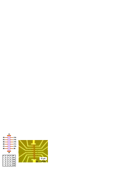
A m long, wide and nm thick multigraphene sample was contacted with 14 electrodes prepared by electron-beam lithography and Pd/Au deposition, see Fig. 1. For the determination of the absolute value of the mean free path the distance between electrodes is of importance; each electrode had a width of m. Taking the distance between the middle point of the electrodes we have then m. The multigraphene sample was prepared by a rubbing and a ultrasound method described in Ref. Barzola-Quiquia et al., 2008 and from a HOPG sample with rocking curve width. Micro-Raman measurements indicate that even samples of 10 nm thickness are of good quality without showing any contribution of the defect-related D-peak at 1350 cm-1 García et al. (2011).
With an AC bridge from Linear Research (LR700) we measured the resistance at different temperatures and at different lengths between voltage electrodes. The inset in Fig. 1 shows the different configuration channels. For example, channel 1 means input current at electrodes 1 and 2 and voltage measurements at electrodes 3 and 4. The results we discuss below are independent whether we take the electrodes array at the right or left of the sample, i.e. 3 and 4 or 14 and 13 (see inset in Fig. 1) indicating a homogeneous behavior of the sample and the current distribution. The used input AC current was A in all the measurements.
III Results
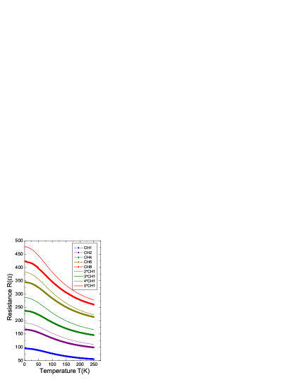
Figures 2 and 3 show the temperature dependence of the absolute and normalized resistance of the sample at different channels, respectively. In Fig. 2 we also show the expected of the channels CH2 to CH8 if the resistance would be just proportional to the distance between voltage electrodes, i.e. , with . As one can clearly recognize in that figure, none of the measured curves follows the expected diffusive Ohmic behavior but are below the one expected. This disagreement is independent of the effective value of , i.e. whether we take it between the middle points of the electrode widths or just between the nearest edges (m).
Taking into account that the width of the sample is not constant but decreases with the channel number, see Fig. 1, the expected and according to Ohm’s law should be even larger, i.e. , where m is the width at channel 1 and an average width between the measured width at electrode 3 () and the width at the corresponding end electrode of the channel . This width can be estimated either by the geometric mean or a simple average, i.e. or , The small differences between the two effective widths change only slightly the absolute estimate of the mean free path and are not relevant.
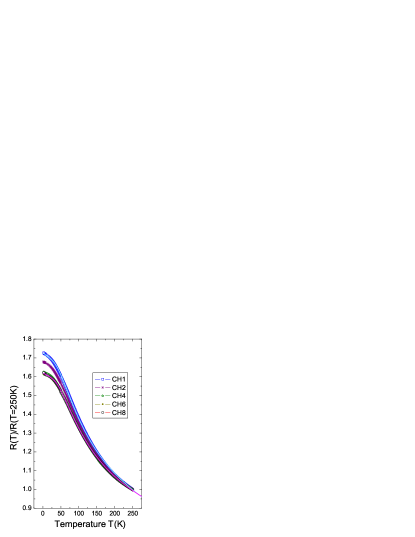
The failure of the diffusive Ohm’s law to describe the data can be also recognized in Fig. 3. In the scale of this figure the larger the distance between electrodes the better is the normalization. As we will see below this is exactly what we expect if the ballistic transport plays a role in the observed behavior. Note that the semiconducting-like behavior with a saturation at low temperatures is observed at all distances between the voltage electrodes indicating that this dependence is intrinsic and not related to the sample size, supporting the conclusions of Ref. García et al., 2011. In fact, using the same parallel resistance model and the exponential temperature dependence appropriate for semiconductors as in Ref. García et al., 2011, the obtained energy gap K is independent of the distance between electrodes.
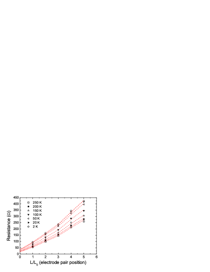
Figure 4 shows the absolute resistance as a function of the channel length at different temperatures. The experimental points appear to be consistently non-linear, curving up with the distance to the first channel. The reason for the observed dependence is explained below and allows us to obtain the carrier mean free path.
According to Sharvin-Knudsen formula and Ohm’s law, the resistance of the sample in terms of geometrical parameters and the resistivity , is given by
| (1) |
where is the mean free path, the thickness, the width of the sample and the distance between the voltage electrodes for each of the selected channels. Defining the ballistic resistance as the first term in Eq. (1), taking into account the effective channel width , assuming homogeneous resistivity and thickness through the whole sample length, this equation can be rewritten as:
| (2) |
where the width at channel 1 is m, ’s are estimated as explained above and .
With the measured widths the experimental data shown in Fig. 4 can be very well fitted using Eq. (2) having as the only free parameter. To obtain the mean free path from we need to calculate the resistivity . This last is obtained from:
| (3) |
and therefore the mean free path is calculated from:
| (4) |
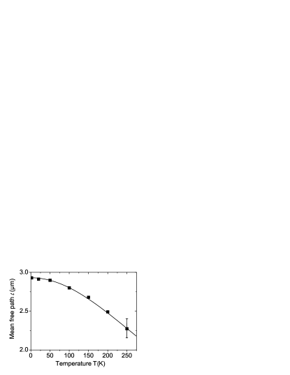
Using Eqs. (3) we obtain Kcm, where the error is due to the errors in the geometry parameters and . The mean free path obtained from Eq. (4) and as a function of the temperature is shown in Fig. 5. Note that the obtained mean free path is independent of the values of the width and thickness of the sample and the statistical error is that of from the fits in Fig. 4. Within experimental error the temperature dependence follows a simple parallel resistance model, i.e. ( in K and in m), with a temperature dependent term given by , similar to that found in HOPG bulk samplesGarcía et al. (2008). This dependence suggests that electron-electron interaction can be the main temperature dependent scattering process.
The error in the absolute value of the mean free path obtained in this work resides mainly in the uncertainty of . One may speculate that the Pd/Au deposited electrodes are invasive and may affect the current distribution and in this case m. On the other hand the electrodes may affect only the upper most graphene layer from the graphene layers inside the rest of the sample. Also, the effective resistance of the polycrystalline Pd film electrode contacting the upper most graphene layer along its m width is not necessarily smaller than the mainly ballistic resistance of the graphene layer. Therefore, taking the electrode width as the maximum uncertainty in we estimate as the largest absolute error in the mean free path.
With the knowledge of the mean free path and the resistivity of the sample we can calculate the Fermi wavelength and the mobility of the carriers using the equations and where is the distance between graphene planes in Bernal graphite and the other parameters are the usual natural constants. At 2 K (250 K) we obtain m and cm2V-1s-1 with a maximum error of 50% in the absolute values.
IV Conclusion
The aim of this experimental work was to show in a single multigraphene sample of large enough length that the resistance does not follow the Ohm law. It does not increase strictly proportional to the distance between voltage contacts, as one would expect from the usual diffusive Ohm law. Instead, we show experimentally that a length independent contribution to the resistance due to the ballistic transport of the carries needs to be considered. From our measurements and with the help of the Sharvin-Knudsen formula for ballistic transport we are able to obtain the mean free path of the carriers at different temperatures and without free parameters. The obtained results support previous results and indicate that the graphene layers within the graphite structure have micrometer large mean free path and Fermi wavelength and mobility cm2V-1s-1 at 300 K. We also conclude that for multigraphene samples of good quality and of size in the micrometer range, a significant error in the estimate of the resistivity is done if the ballistic contribution is not taken into account. Clearly, the results indicate that the Boltzmann-Drude approach to obtain electronic parameters from transport measurements is not adequate.
This work was supported by the DFG under ES 86/16-1. S.D. is supported by the Graduate School of Natural Sciences “BuildMona”.
References
- Kong et al. (2001) J. Kong, E. Yenilmez, T. W. Tombler, W. Kim, H. Dai, R. B. Laughlin, L. Liu, C. S. Jayanthi, and S. Y. Wu, Phys. Rev. Lett. 87, 106801 (2001).
- Liang et al. (2001) W. Liang, M. Bockrath, D. Bozovic, J. H. Hafner, and M. Tinkham, Nature 411, 665 (2001).
- Javey et al. (2004) A. Javey, J. Guo, M. Paulsson, D. Wang, Q. andMann, M. Lundstrom, and H. Dai, Phys. Rev. Lett. 92, 106804 (2004).
- Parendo et al. (2004) K. A. Parendo, L. M. Hernandez, A. Bhattacharya, and A. M. Goldman, Phys. Rev. B 70, 212510 (2004).
- Gao et al. (2005) B. Gao, Y. F. Chen, M. S. Fuhrer, D. C. Glattli, and A. Bachtold, Phys. Rev. Lett. 95, 196802 (2005).
- Purewal et al. (2007) M. S. Purewal, B. H. Hong, A. Ravi, B. Chandra, J. Hone, and P. Kim, Phys. Rev. Lett. 98, 186808 (2007).
- Bolotin et al. (2008) K. I. Bolotin, K. J. Sikes, Z. Jiang, M. Klima, G. Fudenberg, J. Hone, P. Kim, and H. L. Stormer, Solid State Commun. 146, 351 (2008).
- Du et al. (2008) X. Du, I. Skachko, A. Barker, and E. Y. Andrei, Nature Nanotech. 3, 491 (2008).
- García et al. (2008) N. García, P. Esquinazi, J. Barzola-Quiquia, B. Ming, and D. Spoddig, Phys. Rev. B 78, 035413 (2008).
- Dusari et al. (2011) S. Dusari, J. Barzola-Quiquia, P. Esquinazi, and N. García, Phys. Rev. B 83, 125402 (2011).
- Barzola-Quiquia et al. (2010) J. Barzola-Quiquia, S. Dusari, G. Bridoux, F. Bern, A. Molle, and P. Esquinazi, Nanotechnology 21, 145306 (2010).
- Barzola-Quiquia et al. (2008) J. Barzola-Quiquia, J.-L. Yao, P. Rödiger, K. Schindler, and P. Esquinazi, phys. stat. sol. (a) 205, 2924 (2008).
- García et al. (2011) N. García, P. Esquinazi, J. Barzola-Quiquia, and S. Dusari (2011), arXiv:1106.0437.