Magnetic confinement of neutral atoms based on patterned vortex distributions in superconducting disks and rings
Abstract
We propose and analyze neutral atom traps generated by vortices imprinted by magnetic field pulse sequences in type-II superconducting disks and rings. We compute the supercurrent distribution and magnetic field resulting from the vortices in the superconductor. Different patterns of vortices can be written by versatile loading field sequences. We discuss in detail procedures to generate quadrupole traps, self-sufficient traps and ring traps based on superconducting disks and rings. The ease of creating these traps and the low current noise in supercurrent carrying structures makes our approach attractive for designing atom chip interferometers and probes.
pacs:
37.10.Gh, 03.75.Be, 74.78.NaI Introduction
Recently superconducting atom chips have generated a lot of interest due to their attractive properties, such as the Meissner effect for type-I superconductors and vortices for type-II superconductors Cano et al. (2008a, b); Emmert et al. (2009a). Cold atoms have been trapped and manipulated near superconducting surfaces Mukai et al. (2007); Nirrengarten et al. (2006); Emmert et al. (2009a) and Bose-Einstein condensation (BEC) on a superconducting atom chip has been reported recently Roux et al. (2008). Thermal and technical noise in proximity to superconducting surfaces have been shown both theoretically and experimentally to be significantly reduced compared to conventional atom chips Scheel et al. (2005); Skagerstam et al. (2006); Hohenester et al. (2007); Nogues et al. (2009); Hufnagel et al. (2009); Kasch et al. (2010); Emmert et al. (2009b); Fermani et al. (2010). Superconducting atom chips have the potential to coherently interface atomic and molecular quantum systems with quantum solid state devices Tian et al. (2004); André et al. (2006); Tordrup and Mølmer (2008); Verdú et al. (2009); Sørensen et al. (2004). Furthermore, ultracold atoms can be used to probe properties of superconductors, such as the dynamics of vortices in type-II superconductors Scheel et al. (2007); Shimizu et al. (2009).
Previously we reported on the design and realization of several types of magnetic traps involving linear type-II superconducting microstructures Zhang et al. (2010); Müller et al. (2010a, b). These traps are formed by the magnetic field carried by vortices imprinted in the superconductor to confine ultracold atoms. Loading of the vortices is accomplished by tailored external magnetic pulse sequences applied to the superconductor in the mixed state. In a different approach vortex-based magnetic traps have been observed after cooling a superconducting disk through the critical temperature in the presence of an external magnetic field Shimizu et al. (2009).
In this article, we extend our investigation of vortex based microtrap geometries to type-II superconducting disks and rings. To this end we have developed a numerical approach to calculate the vortex patterns imprinted after applying various external magnetic field pulses to the superconducting structure. Using this numerical approach we design quadrupole traps, self-sufficient traps and ring traps in the various superconducting geometries. We demonstrate that, by simple application of an additional bias field, a single quadrupole trap may be deformed into a ring. Considering the low current noise expected from the persistent supercurrents generating these traps, and the low thermal noise expected from superconducting atom chips, this method may be an attractive way to generate low-noise on-chip atom interferometry. Compared to other low noise traps generated by permanent magnets our system retains one desirable feature: The ability to control the trap parameters and geometry from shot to shot.
The paper is organized as follows. Sec. II describes the equations of motion for the sheet current density in a type-II superconducting strip, disk and ring in an external magnetic field. To validate our numerical approach we compute the supercurrents in a superconducting strip, and compare them with analytical results Zhang et al. (2010). For the two-dimensional structures considered in this paper no explicit analytical solution is known. In Sec. III we design several types of traps for cold atoms by tailoring the magnetic field pulses which induce vortex patterns in the superconducting disk and ring. Sec. IV summarizes our results.
II Loading vortices
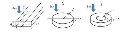
Consider a type-II thin superconducting strip, disk and ring in a magnetic field perpendicular to their surface ( plane) as shown in fig.1. Here denotes the thickness of the superconductors and denotes the half width of the strip and the (outer) radius of the disk and ring. The strip is assumed to be infinitely long along , so that we can restrict our simulation to the plane. Similarly, we can reduce our simulation to the plane for the disk and ring due to rotational symmetry. Throughout the paper we will assume that the temperature of the superconductors is below the critical value and that the thickness is small compared to the other length scales of the system. When the external field exceeds the lower critical field , but lies below the upper critical value , magnetic flux starts to penetrate the superconductor in the form of Abrikosov vortices Abrikosov (2004). To facilitate our numerical analysis we model these vortices together with the screening current as a macroscopic supercurrent . Our approach closely follows the method outlined in Brandt (1994, 1995) which makes use of the continuum approximation where the flux line spacing and the magnetic field penetration depth are small compared to all other relevant length scales considered Brandt (1999). From the distribution of the supercurrent we then compute the total magnetic field outside of the superconductor using the Biot-Savart law. We approximate the current density in the superconductor to be constant over its thickness , which is valid in the thin-film approximation where is smaller than the London penetration depth of the superconductor. The sheet current density is then defined as , where is the local current density.
The perpendicular field component generated in the specimen plane by a constant and by the sheet current along for the strip can be written as Brandt (1994):
| (1) |
For cylindrically symmetric structures, where is circling clockwise, we can write the perpendicular magnetic field component with for disks and for rings as Brandt (1994):
| (2) |
where and are the first and second kind of the complete elliptic integrals with and is the vacuum permeability Brandt (1994, 1995). In order to find an expression for the sheet current density we take into account the time-dependence of and use Maxwell’s equations, to arrive at the equation of motion for the sheet current density of the strip Brandt (1994):
| (3) |
and for disks and rings Brandt (1994):
| (4) |
where
| (5) |
Here, is the nonlinear resistivity with critical value , and where is the characteristic activation energy of the superconductor Blatter et al. (1994). is the critical sheet current density Brandt (1994, 1995), defined as the maximum current density the superconductor can carry without a transition into the normal state. For the scope of this paper we have chosen the value of . This value gives a moderate response of the superconductor to applied fields. The exact value for is material dependent and does not qualitatively alter the characteristic current distributions discussed for the experimentally applicable values.
We approximate the integration in Eq.3 and 4 by a Riemann Sum. First, we discretise the width of the strip and disk (or ring) into N elements with the same size or (), and denote the middle point of each element by or , . Then we rewrite Eq.3 in the form of a Riemann Sum in matrix form
| (6) |
To solve the differential equation, we invert Eq.6 to find an equation for
| (7) |
where is the inverse of the matrix . Now, we can use the Euler method and the initial conditions and to compute the sheet current density at by
| (8) |
where . The same approach can be used for Eq.4. From the above Eq.8, we can see that the final sheet current density is only dependent on the initial conditions and , not on . After we obtain , we compute the field outside of the superconducting film () using the Biot-Savart law.
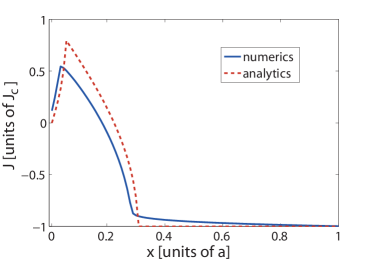
In order to validate our numerical model, we consider the case of vortices induced in a superconducting strip, for which an analytical solution exists Zhang et al. (2010). Applying a magnetic field pulse with a magnitude of perpendicular to the strip surface, the magnetic flux penetrates the strip. We solve Eq.3 numerically and obtain the distribution of supercurrents in the strip plotted in Fig.2 (solid lines). The small difference in the curves arises from the fact that the analytical solution assumes that at the edge, where the magnetic flux penetrates, the sheet current density takes the critical value. For the numerical computation the sheet current density is completely determined by Eq.3.
III Magnetic traps
In this section, we apply Eq.4 to compute the sheet current density induced in the superconducting disk and ring by various loading fields. From the distribution of the sheet current density we then compute the magnetic field carried by the vortices by means of the Biot-Savart law. An intuitive picture of the vortex loading process can be found in Bean (1964).
III.1 Traps generated by a superconducting disk
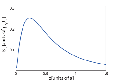
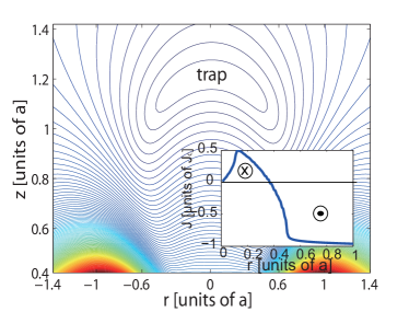
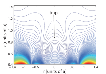
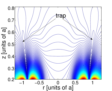
Consider a disk shaped superconductor in the remanent state with a magnetic loading field pulse of . The second critical field in our calculations is approximately . For symmetry reasons the radial component of the total external field is always zero above the disk center. The component of the total external field above the disk center at different heights is plotted in Fig.3. is always zero at the surface center of the disk , because the superconductor prevents any magnetic field perpendicular to its surface at this point. The inset of Fig.4 shows the supercurrent distribution obtained from Eq.4. We see that the supercurrent in the disk is separated into two regions; one with current propagating clockwise and one with current in the counter-clockwise direction. Applying a small bias field on the order of perpendicular to the disk, allows us to cancel at and create a quadrupole trap for low-field seeking atoms. Fig.4 shows such a trap for and . Increasing the bias field will move this trap closer to the disk surface, however in doing so the bias field will also induce currents into the disk, ensuring that the field at the disk surface center remains 0. This puts a dependent limit on the trap depth for traps created very close to the disk surface.
The superconductor has a memory of the history of the external fields. Therefore it is possible to design a pulse sequence in which the role of the bias field is assumed by another induced supercurrent carried by the disk. Here we use two loading pulses with amplitudes of and respectively to write a vortex pattern in the disk, which results in a self-sufficient trap above the disk center, as shown in Fig.5. Choosing typical experimental values for the critical current density of YBCO at liquid Nitrogen temperatures we calculate a self-sufficient trap depth of for a disk with a diameter of . This trap has the feature of transforming into a ring trap by applying an additional perpendicular bias field .
While it is possible to split the self-sufficient trap into a ring, it does not necessarily imply a simple loading procedure with a high transfer efficiency from an external trap via the self-sufficient trap. A more straightforward way of producing a ring trap from an external quadrupole trap is to use a first magnetic field pulse of followed by a second pulse . Due to the nonlinear response of the material, this pulse sequence does not result in a self-sufficient trap, and instead a quadrupole trap can be formed far away from the chip surface by applying an additional bias field . By increasing the value of this trap is brought closer to the chip surface where it eventually deforms into a ring trap.
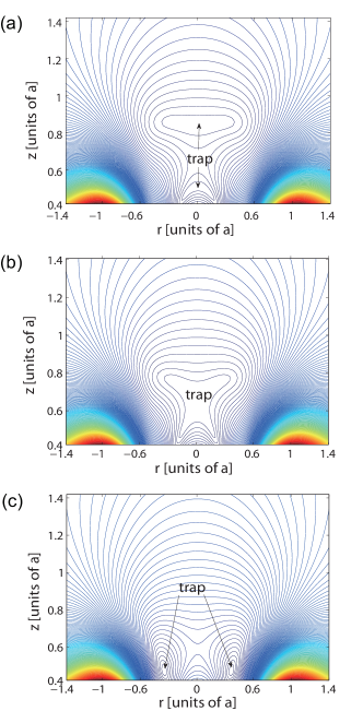
The perpendicular bias field lifts the field zero on the disk surface and lowers the quadrupole trap, producing two traps above the disk center, see Fig.6(a). Increasing the bias field brings the two traps closer together, until they merge at , see Fig.6(b). Increasing further will turn the trap into a ring trap, as shown in Fig.6(c). Continuing to increase increases the radius of the ring trap until the trap is lowered to the surface.
III.2 Traps generated by a superconducting ring
In this section we consider an annular superconductor. The inset of Fig.8(a) shows the supercurrents carried by the vortices in the remanent state, when we apply a field pulse with a magnitude of to a superconducting ring.
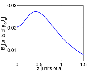
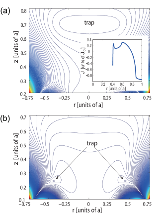
Similar to the superconducting disk, is always zero by symmetry. We plot the component of the magnetic field generated by these supercurrents at different height in Fig.7. If an additional perpendicular field is applied to cancel , a quadrupole trap can be formed at . When a quadrupole trap is formed at , as shown in Fig.8(a). For small bias fields, increasing the magnitude of reduces the trap distance to the chip surface. When , the quadrupole trap transforms into a ring trap, as shown in Fig.8(b). Further increasing the bias field will enlarge the radius of the ring trap until the trap is lowered to the surface.
Alternatively, a ring trap may be formed by applying two field pulses and a bias field as indicated in Fig.9. The first pulse has a magnitude of , the second has a magnitude of and the bias field . The ring trap of Fig.9 has a larger radius and distance to the surface as well as tighter confinement than the one shown in Fig.8(b).
IV Conclusion
We have investigated and designed a variety of confining geometries for ultra cold neutral atoms based on type-II superconducting disk and ring structures. These geometries include quadrupole traps, a self-sufficient trap and ring traps. We have shown that a quadrupole trap above a superconducting disk and ring can be formed by applying a single magnetic field loading pulse and adding an external bias field. Using a double pulse sequence we are able to produce a self-sufficient trap above the disk center. We have developed a procedure for the formation of ring traps based on superconducting disk and ring structures. Furthermore we have shown an efficient loading procedure for these ring traps. Apart from methods outlined in this paper based on superconductors in the mixed state, it is possible to produce quadrupole traps with a ring-shaped superconductor in the Meissner state using flux trapped inside the ring and a bias field. By varying the trapped flux and bias field magnitudes ring traps can be produced. However, the limitations on the imprinted current distribution make it impossible to generate versatile magnetic field patterns Brandt and Clem (2004). The key point of using type-II superconducting structures is that a single microstructured element is capable of generating tailored complex trap geometries for a variety of experimental implementations. This allows us to control the geometry of confining potentials and their parameters without having to fabricate a new atom chip. In addition to this flexibility, superconductors have the intrinsic advantage of a low trap loss rate due to the reduced spin flips of the atoms close to the chip surface. The potential contribution to the spin flip rate by vortex motion in the superconductor has yet to be experimentally investigated.
An additional control over the trap geometries, complementary to the magnetic field pulses, can be obtained by dressing the atomic states with a radio-frequency field Hofferberth et al. (2006); Fernholz et al. (2007). This can help to lift the magnetic field zero intrinsically present in quadrupole traps, thus reducing the Majorana spin flip rate. The low field noise in the proposed ring traps may make them an attractive candidate for the construction of a Sagnac-type interferometer Arnold et al. (2006). A persistent flow of ultracold atoms, even an analog of the superconducting quantum interference device (SQUID), may be realized in these ring traps Ryu et al. (2007); Ramanathan et al. (2011). Taking into account all the intrinsic advantages discussed highlights the potential of magnetic traps for neutral atoms based on patterned vortex distributions in superconducting disks and rings.
Acknowledgements.
We acknowledge financial support from Nanyang Technological University (grant no. WBS M58110036), A-Star (grant no. SERC 072 101 0035 and WBS R-144-000-189-305) and the Centre for Quantum Technologies, Singapore. We thank S.A. Cheong for fruitful discussion.References
- Cano et al. (2008a) D. Cano, B. Kasch, H. Hattermann, D. Koelle, R. Kleiner, C. Zimmermann, and J. Fortágh, Phys. Rev. A 77, 063408 (2008a).
- Cano et al. (2008b) D. Cano, B. Kasch, H. Hattermann, R. Kleiner, C. Zimmermann, D. Koelle, and J. Fortágh, Phys. Rev. Lett. 101, 183006 (2008b).
- Emmert et al. (2009a) A. Emmert, A. Lupaşcu, M. Brune, J.-M. Raimond, S. Haroche, and G. Nogues, Phys. Rev. A 80, 061604(R) (2009a).
- Mukai et al. (2007) T. Mukai, C. Hufnagel, A. Kasper, T. Meno, A. Tsukada, K. Semba, and F. Shimizu, Phys. Rev. Lett. 98, 260407 (2007).
- Nirrengarten et al. (2006) T. Nirrengarten, A. Qarry, C. Roux, A. Emmert, G. Nogues, M. Brune, J.-M. Raimond, and S. Haroche, Phys. Rev. Lett. 97, 200405 (2006).
- Roux et al. (2008) C. Roux, A. Emmert, A. Lupaşcu, T. Nirrengarten, G. Nogues, M. Brune, J.-M. Raimond, and S. Haroche, Eur. Phys. Lett. 81, 56004 (2008).
- Scheel et al. (2005) S. Scheel, P. K. Rekdal, P. L. Knight, and E. A. Hinds, Phys. Rev. A 72, 042901 (2005).
- Skagerstam et al. (2006) B.-S. K. Skagerstam, U. Hohenester, A. Eiguren, and P. K. Rekdal, Phys. Rev. Lett. 97, 070401 (2006).
- Hohenester et al. (2007) U. Hohenester, A. Eiguren, S. Scheel, and E. A. Hinds, Phys. Rev. A 76 (2007).
- Nogues et al. (2009) G. Nogues, C. Roux, T. Nirrengarten, A. Lupaşcu, A. Emmert, M. Brune, J. M. Raimond, S. Haroche, B. Plaçais, and J.-J. Greffet, Europhys. Lett. 87, 13002 (2009).
- Hufnagel et al. (2009) C. Hufnagel, T. Mukai, and F. Shimizu, Phys. Rev. A 79, 053641 (2009).
- Kasch et al. (2010) B. Kasch, H. Hattermann, D. Cano, T. E. Judd, S. Scheel, C. Zimmermann, R. Kleiner, D. Kölle, and J. Fortágh, New. J. Phys. 12, 065024 (2010).
- Emmert et al. (2009b) A. Emmert, A. Lupaşcu, G. Nogues, M. Brune, J.-M. Raimond, and S. Haroche, Eur. Phys. J. D 51, 173 (2009b).
- Fermani et al. (2010) R. Fermani, T. Müller, B. Zhang, M. J. Lim, and R. Dumke, J. Phys. B (2010), 43, 095002 (2010).
- Tian et al. (2004) L. Tian, P. Rabl, R. Blatt, and P. Zoller, Phys. Rev. Lett. 92, 247902 (2004).
- André et al. (2006) A. André, D. DeMille, J. M. Doyle, M. D. Lukin, S. E. Maxwell, P.Rabl, R. J. Schoelkopf, and P. Zoller, Nature Phys. 2, 636 (2006).
- Tordrup and Mølmer (2008) K. Tordrup and K. Mølmer, Phys. Rev. A 77, 020301(R) (2008).
- Verdú et al. (2009) J. Verdú, H. Zoubi, Ch. Koller, J. Majer, H. Ritsch, and J. Schmiedmayer, Phys. Rev. Lett. 103, 043603 (2009).
- Sørensen et al. (2004) A. S. Sørensen, C. H. van der Wal, L. I. Childress, and M. D. Lukin, Phys. Rev. Lett. 92, 063601 (2004).
- Scheel et al. (2007) S. Scheel, R. Fermani, and E. A. Hinds, Phys. Rev. A 75, 064901 (2007).
- Shimizu et al. (2009) F. Shimizu, C. Hufnagel, and T. Mukai, Phys. Rev. Lett. 103, 253002 (2009).
- Zhang et al. (2010) B. Zhang, R. Fermani, T. Müller, M. J. Lim, and R. Dumke, Phys. Rev. A 81, 063408 (2010).
- Müller et al. (2010a) T. Müller, B. Zhang, R. Fermani, K. S. Chan, Z. W. Wang, C. B. Zhang, M. J. Lim, and R. Dumke, New. J. Phys. 12, 043016 (2010a).
- Müller et al. (2010b) T. Müller, B. Zhang, R. Fermani, K. S. Chan, Z. W. Wang, C. B. Zhang, M. J. Lim, and R. Dumke, Phys. Rev. A 81, 053624 (2010b).
- Abrikosov (2004) A. A. Abrikosov, Rev. Mod. Phys. 76, 975 (2004).
- Brandt (1994) E. H. Brandt, Phys. Rev. B 50, 4034 (1994).
- Brandt (1995) E. H. Brandt, Phys. Rev. B 52, 15442 (1995).
- Brandt (1999) E. H. Brandt, Physical Review B 59, 3369 (1999).
- Blatter et al. (1994) G. Blatter, M. V. Feigel’man, V. B. Geshkenbein, A. I. Larkin, and V. M. Vinokur, Reviews of Modern Physics 66, 1125 (1994).
- Bean (1964) C. Bean, Rev. Mod. Phys. 36 (1964).
- Brandt and Clem (2004) E. H. Brandt and J. R. Clem, Physical Review B 69, 184509 (2004).
- Hofferberth et al. (2006) S. Hofferberth, I. Lesanovsky, B. Fischer, J. Verdu, and J. Schmiedmayer, Nature Physics 2, 710 (2006).
- Fernholz et al. (2007) T. Fernholz, R. Gerritsma, P. Krüger, and R. J. C. Spreeuw, Physical Review A 75, 063406 (2007).
- Arnold et al. (2006) A. S. Arnold, C. S. Garvie, and E. Riis, Phys. Rev. A 73, 041606 (2006).
- Ryu et al. (2007) C. Ryu, M. F. Andersen, P. Cladé, V. Natarajan, K. Helmerson, and W. D. Phillips, Phys. Rev. Lett. 99, 260401 (2007).
- Ramanathan et al. (2011) A. Ramanathan, K. C. Wright, S. R. Muniz, M. Zelan, W. T. Hill, C. J. Lobb, K. Helmerson, W. D. Phillips, and G. K. Campbell, Phys. Rev. Lett. 106, 130401 (2011).