Intermediate state switching dynamics in magnetic double layer nanopillars grown by molecular beam epitaxy
Abstract
We observe a stable intermediate resistance switching state in the current perpendicular to plane geometry for all Co/Cu/Co double layer nanopillar junctions grown by molecular beam epitaxy. This novel state has a resistance between the resistances of the parallel and antiparallel alignment of both Co-layer magnetizations. The state, which originates from an additional in-plane magnetic easy axis, can be reached by spin transfer torque switching or by an external magnetic field. In addition to spin torque-induced coherent small-angle spin wave modes we observe a broad microwave emission spectrum. The latter is attributed to incoherent magnetic excitations that lead to a switching between the intermediate state and the parallel or antiparallel alignment of both ferromagnetic layers. We conclude that the additional magnetic easy axis suppresses a stable trajectory of coherent large-angle precession, which is not observed in our samples.
keywords:
1 Introduction
A spin-polarized current passing through a ferromagnetic layer can exert a spin transfer torque on its magnetization [1, 2, 3, 4, 5]. The torque is of particular interest, since it opens the way to an efficient control of the magnetic moments of a nanomagnet in applications such as nonvolatile magnetic memories and tunable microwave oscillators. Most previous work has been focused on polycrystalline nanopillars consisting of ferromagnet/normal metal/ferromagnet (FM/NM/FM) layered systems with unequal FM layer thicknesses. The thicker FM layer is used to spin-polarize the current when flowing in the perpendicular-to-plane direction. The second NM/FM interface may exhibit a net spin torque on the thinner FM due to the absorption of a transverse spin component. Depending on both the current and the external magnetic field the spin torque can either switch the thin FM layer hysteretically between the parallel (P) and antiparallel (AP) alignment of both magnetizations [6] or excite the thin layer in a variety of distinguishable dynamical modes [7, 8, 9]. In epitaxial bilayer samples, however, magneto-crystalline anisotropy can reveal an additional anisotropy axis resulting in two-step magnetization switching effects [10, 11].
In this work, we study Co/Cu/Co-nanopillars grown by molecular beam epitaxy (MBE) using quasi-static and high-frequency resistance measurements at room temperature. The goal is to establish a field-current phase diagram of the differential resistance and the microwave emission of theses junctions. We observe a stable intermediate resistance state (IS) in between the P and the AP alignment of both ferromagnetic layers. We discuss the origin of the IS and its effect on the magnetization dynamics of the thin Co layer. We find that the novel IS suppresses coherent large-angle precessional magnetization dynamics favoring incoherent magnetization excitations.
2 Materials and methods
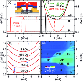
Samples have been fabricated using focused ion-beam assisted nanostencil masks [12, 13]. The thin film stack of Co(3 nm)/Cu/Co(15 nm) is deposited by MBE in prefabricated undercut templates on top of a sputtered Pt bottom electrode (BE) (Fig. 1(a), inset). The presented experimental data have been obtained from a nanopillar with an elliptical cross section of and a 15 nm thick Cu spacer. While we focus in this paper on the results obtained on a single sample, the existence of the intermediate resistance state is independent of the Cu spacer thickness ( nm) and the cross sectional area ( to ). The device is connected to microwave probes and a DC current is injected via a bias-tee, along with a AC current (). The high frequency components of the resistance changes due to magnetization dynamics are analyzed using a spectrum analyzer with a bandwidth between 0.1 and . All measurements are performed at 300 K with an in-plane magnetic field aligned along the easy axis due to the shape anisotropy. For each microwave power spectrum we have subtracted a background spectrum. We define electrons flowing from the thin to the thick Co layer as positive current.
3 Results
Fig. 1(a) shows a typical field-driven magnetoresistance (MR) measurement at small positive current. When is reduced from kOe (red solid line) the dipolar coupling between both Co layers causes the thin layer to switch abruptly already at Oe from the low resistance P state to a higher resistance state. In contrast to previous studies [12, 14] this higher resistance state does not correspond to the AP state but to a novel stable IS with a resistance value lower than the AP state. The latter state is only reached at Oe, which is the coercive field of the thick layer. As the negative is increased further the thin layer switches at Oe in one step to the reversed P configuration. From the switching fields and we can extract [15] the coupling strength between the two FM layers Oe and the coercive field of the thin layer Oe, consistent with previous studies of Co-based nanopillars [7, 14].
In Fig. 1(b) we depict the differential resistance of the junction as a function of for representative values of . The system was first set into the P state at and kOe. For Oe we clearly observe current induced hysteretic switching. In comparison with the field-driven MR (Fig. 1(a)) it is obvious that the high resistance state is not the AP state but rather corresponds to the IS. Note that even for current values up to 15 mA the AP state is not accessible (not shown). Such a behavior has not been observed for sputtered samples [6, 12, 16]. We observe a similar behavior in all our junctions.
For large positive currents and fields we observe the well known peaks in the differential resistance (in Fig. 1(c)), which indicate the onset of spin wave generation in the thin layer [7]. At small magnetic fields (see Oe curve in Fig. 1(b) and (c)) pronounced non-hysteretic dips are seen in the curves. As our sample is in the IS and not in the AP state, it will be interesting to explore the spin wave dynamics in this regime. As the field polarity is inverted (see, e.g., Oe in Fig. 1(b)) the system switches into the AP state. In this state only a small resistance decrease appears at negative .
The current induced transport is summarized in a transport phase diagram in Fig. 1(d). The three distinct resistance states (P, IS, AP) and the expected dynamics regions (D) are marked. The major difference compared to previous phase diagrams of sputtered Co/Cu/Co samples [14, 17] is that our samples can be driven by current only into the IS and not into the AP state. Otherwise the phase diagrams looks quite similar.
To further explore the magnetic configuration of the IS, we have varied the in-plane orientation of the magnetic field. We find that the switching in the field-driven MR always occurs via the IS, independent of the angle between and the magnetic easy axis of the Co layer shape anisotropy (data not shown). Furthermore the IS does not change its resistance value near . This demonstrates that the IS is given by a well defined magnetization configuration of both FM layers and does not originate from a multidomain configuration or a vortex state. A multidomain configuration is also not plausible as we observe the IS in every sample. It is therefore indicative that the magneto-crystalline anisotropy (MCA) of the FM layers might be related to the IS, which becomes relevant in epitaxial layers [18].
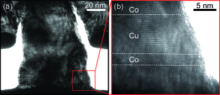
To investigate the crystallinity of our MBE grown nanopillars, we use transmission electron microscopy (TEM). A typical result is shown in Fig. 2 for a layer sequence of Cu(5 nm)/Co(3 nm)/Cu(10 nm)/Co(15 nm)/Cu(70 nm) deposited on top of a Pt bottom electrode. The presented side view image (Fig. 2(a)) demonstrates that the IS does not originate from an artefact of the extended layer stack on top of the Pt hard mask because theses layers are separated from the magnetic nanopillar due to its tapered sidewalls. The high crystallinity of the MBE grown films is visible in the high resolution TEM image in Fig. 2(b) over the full layer stack. Although we cannot determine the in-plane crystal orientation of the layers inside the nanopillar, this result supports the notion that the MCA of the FM layers is relevant for the magnetic switching. From the [111] texture of the Co layers [19] we conclude the existence of additional magnetic easy axes in the layer plane, non-collinear with the easy axis of the shape anisotropy.
Consequently, the magnetic switching of the thin Co layer from the P state into the IS is consistent with switching between the easy axis direction due to the shape anisotropy and an easy axis direction of the MCA. In order to estimate the resulting angle in between both Co-magnetization directions in the IS configuration we use for simplicity the -dependence of the giant magnetoresistance effect for symmetrical systems consisting of 2 identical ferromagnetic layers [20]. For the resistance value of the IS in Fig. 1 (a) this gives an angle of . It is important to emphasize that the relative resistance of the IS does vary from junction to junction for otherwise identical layer stacks. This indicates a variation of the MCA axis relative to the shape anisotropy direction for different junctions which is probably related to a random growth orientation on the sputtered Pt bottom electrode.
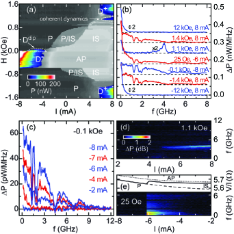
We next focus on the spin torque-induced spin wave dynamics. In Fig. 3 we present frequency domain studies of microwave emission detected near the current induced magnetization instabilities as previously identified in the vs. curves in Fig. 1(b),(c). The correlation between the differential resistance changes and the integrated microwave power is displayed in the microwave emission phase diagram (Fig. 3(a)). It shows different regimes of excitations depending on both current and magnetic field polarity [28]. On the one hand, we observe microwave emission at negative currents in both the dip regime Ddip for small positive fields (Fig. 1(c)) and the D--regime. On the other hand, we detect magnetic excitations at large positive currents and magnetic fields kOe (D+-regimes). These excitations are linked to peaks in (Fig. 1(c)), i.e. to an increase in junction resistance.
In Fig. 3(c) we depict microwave spectra for various negative currents at a small magnetic field of kOe (D--regime). For currents below the emission threshold of mA, we detect microwave emission spectra extending from 100 MHz up to 9 GHz. Their overall amplitude increases with increasing negative current values (Fig. 3(c)), but surprisingly, there is no frequency shift neither with current nor with magnetic field. Note that the sharp minima in observed at several frequencies are visible in all measured spectra independent of current. They are not related to the sample but are rather due to absorption in the high frequency electrical circuit.
Similarly broad emission spectra are also observed in the D+-regimes (see kOe, mA in Fig. 3(b)) as well as in the dip regime Ddip (see Oe emission data in Fig. 3(b) and in Fig. 3(e) with a continuum at low frequencies). In the latter case the microwave emission abruptly disappears near mA when the magnetization configuration switches from the IS into the P state. This switching is reflected in the corresponding change in resistance vs. included in Fig. 3(e). We interpret these broad microwave emission spectra (Fig. 3(b,c,e)) as a result of incoherent spin-wave excitations due to spin transfer torque that lead to a switching [22, 23] between the intermediate state IS and the P or AP state of both ferromagnetic layers. The incoherence is attributed to inhomogeneities in local fields giving rise to distributions of local precession frequencies [8]. Hence, we conclude that the additional easy axis due to the MCA of the thin Co layer suppresses a stable trajectory, i.e. a well defined mode frequency of the coherent large-angle dynamics, which was previously found in polycrystalline samples [17, 7]. Note that the observed incoherent magnetization dynamics has not been reported in frequency domain studies on single-crystalline nanopillars [24].
In addition to the incoherent magnetization dynamics we also observe coherent small angle precessional dynamics of the thin Co layer in a small range of positive magnetic fields for positive currents slightly above the hysteretic switching regime (see kOe, 5 mA mA in Fig. 3(a,b,d)). The spectra have a typical linewidth of MHz. Independent of the magnetic field we only observe spin wave frequencies which increase with increasing current magnitude. Such behavior is characteristic of out-of-plane precessional modes [25]. In contrast, we do not observe in-plane precessions which could be identified by a decrease of their excitation frequency with increasing current [25]. These findings support the notion that in-plane precession of the thin layer magnetization is inhibited by the intermediate state.
For high magnetic fields kOe and large positive currents the microwave emission continuously evolves into a spectrum resembling 1/f noise without any high-frequency peaks. The reason lies in the chaotic character of the incoherent spin wave excitations [8] as seen in Fig. 3(b) for kOe. This regime is correlated with an increase in junction resistance (Fig. 1(c)). The so-called static high resistance state has also been observed previously in systems without an intermediate resistance state [26] and has its origin in an out-of-plane tilted magnetization of the thin Co layer, where the spin torque and the torque by the external magnetic field compensate each other [27, 28, 29]. The out-of-plane tilted magnetization therefore yields a transition to a regime of dynamics not affected by the in-plane anisotropies.
4 Conclusions
In conclusion, MBE-grown Co/Cu/Co magnetic double layer nanopillar junctions show a stable intermediate resistance state with a resistance value between the resistances of the parallel and antiparallel alignments of both Co layers. It results from magnetic switching of the thin Co layer into an additional in-plane easy axis, which is non-collinear with the shape anisotropy axis. We have shown that the additional easy axis may originate from a magneto-crystalline anisotropy due to the texture or enhanced crystallinity of the layer stack. For magnetic fields smaller than the coercive field of the thin Co layer, we observe hysteretic switching between the parallel magnetization configuration and the intermediate resistance state. However, no current induced transitions into the AP state have been observed. Although the current induced resistance changes agree qualitatively with dipolar coupled double magnetic layer nanopillars without an intermediate state, no coherent large-angle precessional motion of the thin-layer magnetization has been observed. Instead we detect broad microwave emission spectra, which we attribute to incoherent excitations that lead to switching between the intermediate state and the parallel or antiparallel magnetization configurations.
We acknowledge useful discussions with B. Özyilmaz. This work was supported by DFG through SPP 1133 and by HGF.
References
- [1] J. C. Slonczewski, J. Magn. Magn. Mater 159 (1996) L1.
- [2] L. Berger, Phys. Rev. B 54 (1996) 9353.
- [3] M. Tsoi, A. G. M. Jansen, J. Bass, et al., Phys. Rev. Lett. 80 (1998) 4281.
- [4] E. B. Myers, D. C. Ralph, J. A. Katine, et al., Science 285 (1999) 867.
- [5] M. D. Stiles, A. Zangwill, Phys. Rev. B 66 (2002) 014407.
- [6] J. A. Katine, F. J. Albert, R. A. Buhrman, et al., Phys. Rev. Lett. 84 (2000) 3149.
- [7] S. I. Kiselev, J. C. Sankey, I. N. Krivorotov, et al., Nature 425 (2003) 380.
- [8] K.-J. Lee, A. Deac, O. Redon, et al., Nature Mat. 3 (2004) 877.
- [9] S. I. Kiselev, J. C. Sankey, I. N. Krivorotov, et al., Phys. Rev. Lett. 93 (2004) 036601.
- [10] H. Dassow, R. Lehndorff, D. E. Bürgler, et al., Appl. Phys. Lett. 89 (2006) 222511.
- [11] R. Lehndorff, M. Buchmeier, D. E. Bürgler, et al. Phys. Rev. B 76 (2007) 214420.
- [12] B. Özyilmaz, G. Richter, N. Müsgens, et al., J. Appl. Phys. 101 (2007) 063920.
- [13] N. Müsgens, E. Maynicke, M. Weidenbach, et al., J. Phys. D 41 (2008) 164011.
- [14] S. Urazhdin, H. Kurt, J. W. P. Pratt, et al., Appl. Phys. Lett. 83 (2003) 114.
- [15] ; .
- [16] F. J. Albert, J. A. Katine, R. A. Buhrman, et al., Appl. Phys. Lett. 77 (2000) 3809.
- [17] J. C. Sankey, I. N. Krivorotov, S. I. Kiselev, et al., Phys. Rev. B 72 (2005) 224427.
- [18] R. Lehndorff, D. E. Bürgler, S. Gliga, et al., Phys. Rev. B 80 (2009) 054412.
- [19] XRD measurements (not shown) of extended Pt/Cu/Co/Cu layers do reveal a faint [111] texture perpendicular to the layer plane. Similar texture has been observed for Co1-xPtx alloys on Pt layers by D. Weller et al., Appl. Phys. Lett. 61, 2726 (1992). The texture gives rise to a hexagonal symmetry of the Co layer.
- [20] J. C. Slonczewski, J. Magn. Magn. Mater. 247 (2002) 324.
- [21] J. Xiao, A. Zangwill, M. D. Stiles, Phys. Rev. B 72 (2005) 014446.
- [22] S. Urazhdin, N. O. Birge, W. P. Pratt, et al., Phys. Rev. Lett. 91 (2003) 146803.
- [23] A. Fábián, C. Terrier, S. S. Guisan, X. Hoffer, et al., Phys. Rev. Lett. 91 (2003) 257209.
- [24] R. Lehndorff, D. Burgler, A. Kakay, et al., IEEE Transact. on Magn. 44 (2008) 1951.
- [25] M. D. Stiles, J. Miltat, Topics in Applied Physics 101 (2006) 225.
- [26] S. I. Kiselev, J. C. Sankey, I. N. Krivorotov,et al., Phys. Rev. B 72 (2005) 064430.
- [27] Z. Li, S. Zhang, Phys. Rev. B 68 (2003) 024404.
- [28] J. Xiao, A. Zangwill, M. D. Stiles, Phys. Rev. B 70 (2004) 172405.
- [29] A. N. Slavin, V. S. Tiberkevich, Phys. Rev. B 72 (2005) 094428.