First-principles study of native point defects in topological insulator Bi2Se3
Abstract
The p-type Bi2Se3 is much desirable as a promising thermoelectric material and topological insulator, while the naturally grown Bi2Se3 is always n-type doped by native point defects. Here we use first-principles calculations to identify the origin of the n-type tendency in bulk Bi2Se3: The Se vacancies (V and V) and Se antisite dominate the donorlike doping with low formation energy, while the predisposed Bi defect results in the pair of V and Bi interstitial, which is also a donor rather than an acceptor. Moreover, for Bi2Se3(111) surface, we find that the band structures modulated by the defects explicitly account for the existing experimental observations of n-type preference.
pacs:
71.20.-b, 71.70.Ej, 73.20.AtBecause of their excellent thermoelectric performance at room temperature, the layered compound Bi2X3 (X=Se, Te), have long been attracting great interest for decades in condensed-matter physics Mahan1998 ; Kanatzidis2001 . Recently, these materials have been drawing renewed attention by their novel properties as topological insulators, which possess insulating gaps in the bulk and gapless states on surfaces Xia2009 ; Zhang2009 ; Chen2009 ; Tong2009 . Specially, the defects in Bi2Se3 or Bi2Te3 dramatically dominate its thermoelectric and topological properties. For Bi2Te3, it can be simply made n or p type through variation in the Bi:Te ratio. For Bi2Se3, however, one of the major issues has been the difficulty in making the material p type. As revealed by angle resolved photoemission spectroscopy (ARPES), the as-grown Bi2Se3 samples without doping are n-type semiconductors Urazhdin2002 ; Urazhdin2004 ; Xia2009 , mainly owing to the Se vacancies (V defects), or Se substituted defects on Bi sites (Se antisite defects). While the acceptor-like defects such as Bi antisite defect, are rarely observed. Only through doping with extrinsic Ca on the Bi site, one can realize the formation of p-type material Hor2009 .
There have been several existing literatures dealing with the defects in Bi2Se3 Hor2009 ; Urazhdin2002 ; Urazhdin2004 , while previous studies did not investigate its defect structure and formation energy in detail. Therefore a comprehensive studying of the native point defect formation in this material is still lacking. Particularly, the influence of the native point defects on the topological surface states of this material is not much clear yet. In order to deeply understand the novel properties of Bi2Se3, it is instructive to investigate the formation of native defects, which is not only of fundamental conceptual importance, but also paves the way for realizing promising application of Bi2Se3 as a novel topological insulator.
In this letter, by means of first-principles calculations, we present a comprehensive study of native point defects in Bi2Se3, including V vacancies, Se and Bi antisite defects. The structure and formation energy of such defects in bulk Bi2Se3, as well as their band structures, are calculated and discussed in detail, confirming the n-type preference of Bi2Se3. Besides, by analyzing the surface charge distribution and band structure of Bi2Se3(111) surface with various defects, we present the influence of native point defects on the topological surface states.
The calculations are performed within density functional theory using the Vienna ab-initio simulation package (VASP) VASP . The PBE PBE generalized gradient approximation and the projector-augmented wave potential PAW are employed to describe the exchange-correlation energy and the electron-ion interaction, respectively. The spin-orbit interaction (SOI), which has been confirmed to play an important role in the electronic structure of the topological insulator, is included during the calculation.
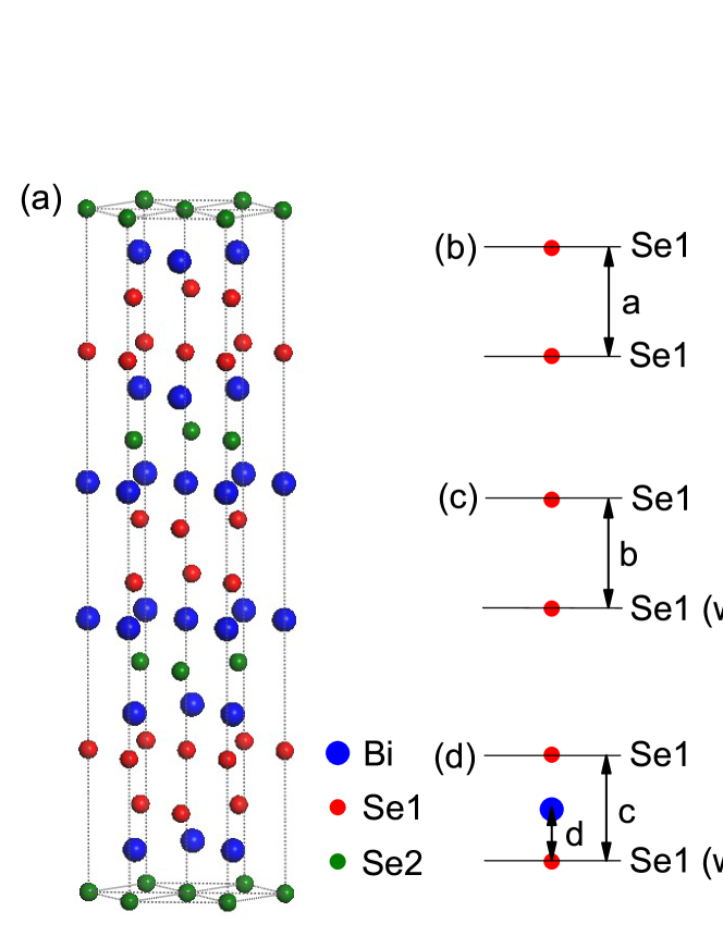
The crystal structure of Bi2Se3 is rhombohedral with the space group (). Equivalently, it can be represented in terms of a hexagonally arranged layer structure, which is shown in Fig. 1(a). The hexagonal unit cell has three sets of quintuple layers, where each quintuple layer consists of five atoms, forming a stable unit Se1-Bi-Se2-Bi-Se1 with strong intrabilayer bonds, while the inter-layer bonding is much weaker. Defect calculations are performed in a 331 supercell with 135 atoms, and integration over the Brillouin zone is done using the Monkhorst-Pack scheme Monkhorst1976 with 552 grid points. The cutoff energy for the plane wave expansion is set to 400 eV, and the structure is fully optimized until the maximum residual ionic force is below 0.02 eV/Å. For the surface calculations, the slabs are modeled by a 6-quintuple layer with the defects adjacent to the surface. The calculated structure parameters of perfect Bi2Se3 are Å, Å, which are close to experimental data Å, ÅNakajima1963 .
The formalism describing the formation energy of point defects in materials has been well established, which depends on the chemical potentials as well as the Fermi level for charged defects. The ranges of chemical potentials for Bi and Se should be evaluated as
| (1) |
| (2) |
where and are chemical potentials for Bi and Se in Bi2Se3, and are chemical potentials of pure Bi and Se, respectively, and is the formation enthalpy of Bi2Se3. The formation energy of a defect X in charge state q is defined as Zhang1991
| (3) |
where is the total energy of the system containing the point defect , is the elemental chemical potential with a positive sign for vacancies and a negative sign for interstitial defects. and are the total energy and valence-band maximum (VBM) of the perfect supercell, respectively. The correction term is added to align the reference potential in the defect supercell with that in the perfect bulk, and is the Fermi level referenced to . Apparently the defect formation energy is function of the atomic chemical potential and Fermi level.

| Defect | Charge | = | = | |||
|---|---|---|---|---|---|---|
| 0 | 0.57 | -0.59 | ||||
| V | +1 | 0.64 | -0.52 | |||
| +2 | 0.68 | -0.48 | ||||
| 0 | 0.94 | -0.23 | ||||
| V | +1 | 0.99 | -0.18 | |||
| +2 | 1.06 | -0.10 | ||||
| 0 | -0.14 | 2.77 | ||||
| Se | +1 | -0.13 | 2.78 | |||
| +2 | -0.03 | 2.88 | ||||
| 0 | 1.54 | -1.37 | ||||
| Bi | -1 | 1.68 | -1.23 | |||
| -2 | 1.85 | -1.06 | ||||
| 0 | 3.05 | 0.14 | ||||
| Bi | -1 | 3.06 | 0.15 | |||
| -2 | 3.07 | 0.15 |
Table 1 summarizes the formation energy of native point defects in various charge state in Bi2Se3 at the VBM (=0 eV) at the Se-rich limit (=) and Bi-rich limit (=), respectively. It is noticeable that for a specific defect the differences in formation energy between different charge states are very tiny, which means that the defects in Bi2Se3 are not evidently charged. Actually, by applying Bader analysis Bader1990 , we can determine the ionic charges of Bi and Se atoms. The value of the calculated Bader charge of the individual Bi, Se1 and Se2 atoms in perfect Bi2Se3 are 0.95e, -0.55e and -0.80e, respectively. It is seen that the differences in electronegativities of these atoms are not large enough to induce charged defect states, quite different from that in other typical semiconductor materials such as ZnO zhang2001 . Therefore, in the following discussion we will only focus on the neutrally charged defect states.
We can find from table 1 that at the Se-rich limit there is only one stable defect, i.e., the Se antsite that has negative formation energy -0.14 eV, consist with the previous experimental observation Urazhdin2002 . At the Bi-rich limit, obviously the Se vacancies with negative formation energy are stable, and V (-0.59 eV) is more energetic favorable than V (-0.23 eV). Correspondingly, stronger structural relaxation in the vicinity of V can be found compared with that of V. For V the inter-layer distance is enlarged to be 3.02 Å(see Fig. 1(c)) compared with 2.99 Å(see Fig. 1(b)) of perfect bulk. While surprisingly, the Bi antisite defect at the Bi-rich limit, which has been considered as the p-type defect thus difficult to form Urazhdin2004 ; Lovett1977 , possesses of the lowest formation energy -1.37 eV. As illustrated in Fig. 1(d), an outwards relaxation of about 1.44 Å for the substituted Bi atom with respect to the Se1 layer is observed, therefore actually the predisposed Bi defect results in a pair of V and Bi interstitial.

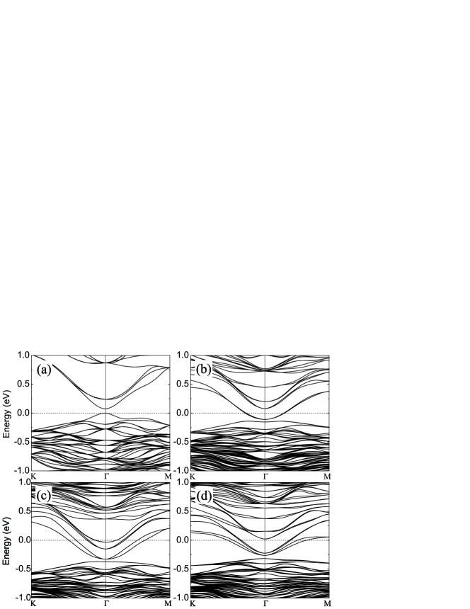
In the following we present the electronic-structure results for bulk Bi2Se3. Figure 2 shows the electronic band structure with and without point defects. For the perfect bulk, our calculation yields a direct band gap of 0.08 eV at point (see Fig. 2(a)), where the difference with the experimental value of 0.2-0.3 eV Mooser1956 ; Black1957 may arise from the deficiency of pseudopotentials adopted. When defects introduced, it is clear that the gap remains robust, while the Fermi level of the system undergoes an evident shift in energy, presenting somewhat metallic behavior. For the bulk with defects V and Se, the Fermi level shifts up for 0.18 and 0.40 eV, respectively (see Fig. 2(b) and (c)). These results are consistent with previous conclusions that Bi2Se3 is naturally n doped Urazhdin2002 ; Urazhdin2004 ; Xia2009 . While for the predisposed Bi defect, the Fermi level shifts up as high as 0.34 eV, implying that Bi2Se3 is also n-type doped. Keeping in mind the much low formation energy and the atomic structure of this kind of defect mentioned above, it is much similar to that in some II-VI semiconductuors Chadi1994 ; Chadi1999 , the pair of V and Bi interstitial in Bi2Se3 forms a stable donor complex (DX) rather than an acceptor.
| Defect | = | = | ||||
|---|---|---|---|---|---|---|
| V | 1.55 | 0.39 | ||||
| Bi | 2.57 | -0.34 | ||||
| Se | 0.35 | 3.26 |
Now that the basic properties of the native point defects in bulk Bi2Se3 have been established. We may ask how these defects affect its topological surface states, as the key important properties of this topological insulator. There exists a rigid difference of the chemical potential by about 200 meV between the experimental result for the naturally n-type sample and theoretical calculation for the stoichiometric Bi2Se3(111) surface Xia2009 . The physic behind this difference is desirable to be investigated. Urazhdin et al. Urazhdin2002 have observed regular clover-shaped features on Bi-doped Bi2Se3(111) surface, and attributed them to the antisite Bi at the bottom of the first quintuple layer. Nevertheless, we believe that there must be other type of defect on the surface. Based on the results about the defects in bulk Bi2Se3, we calculate the atomic and electronic structures of the surfaces with various defects, including V, Se, Bi, as well as the perfect Bi2Se3. In table 2 we list the formation energy of the selected defects on Bi2Se3(111) surface for neutral charge state. It can be seen that Se at Se-rich limit (0.35 eV) and V at Bi-rich limit (0.39 eV) turn out to be unstable compared with that in bulk Bi2Se3. While the defect Bi possesses the lowest formation energy (-0.34 eV) at Bi-rich limit. Moreover, it is noticeable that for Bi, unlike in bulk which forms a DX-like pair, the Bi atom takes the position of Se1 atom, forming the surface antisite defect Bi.
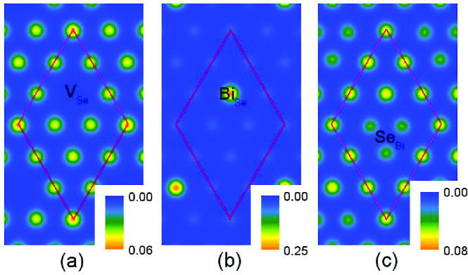
Figure 3 presents the surface charge density distributions of various defects near the surfaces. It is clear that there exists an electron density depletion at the position of V (see Fig. 3(a)). While for the Bi (see Fig. 3(b)), the substituted Bi atom on Se1 position can be easily identified by the electron density accumulation. Because of the low formation energies on (111) surface, and stabilities in bulk Bi2Se3, these two kinds of defects should be easily observed by STM experiment in Bi-doped sample. As for the Se-doped Bi2Se3(111) surface, the Se defect appears as a regular clover-shaped feature (see Fig. 3(c)), with a clear depletion of electron density compared with the perfect surface, which can also be identified by experimental measurements.

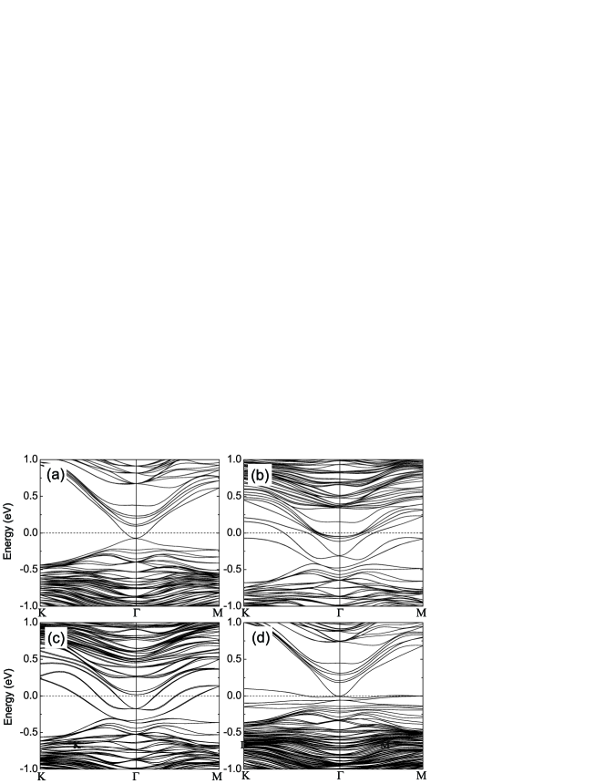
In Fig. 4, we plot the calculated band structures of the Bi2Se3(111) surface with various defects. It can be seen that for the perfect surface without any defect (see Fig. 4 (a)), the topological surface states form a single Dirac cone at the point, implying non-trivial nature of this material. Moreover, the Fermi level is -0.07 eV below the Dirac cone, hence keeping far away from the bulk conduction band, which is much different from the recent ARPES experimental observation that the Fermi level resides in the conduction band Xia2009 , exhibiting naturally n-type feature and presenting the existence of intrinsic defects. To elucidate the experimentally observed shifts of the Fermi level, let us investigate the band structures of the systems with defects. For the V (see Fig. 4 (b)) and Se (see Fig. 4 (c)), the Fermi level of the systems result in rigid shifts up about 0.24 and 0.10 eV compared with the perfect surface, respectively, reaching into the bulk conduction band, hence presenting as donors. Nevertheless, for Bi, the Fermi level almost overlaps with the Dirac point, therefore it does not present evident electron-donor or -acceptor feature. The difference with that in bulk Bi2Se3 may arise from that here the substituted Bi atom just takes the position of Se atom, rather than forming the Bi-V pair.

In conclusion, we have systematically studied the properties of native point defects in topological insulator Bi2Se3. For bulk Bi2Se3, V and Bi defects at the Bi-rich limit were identified to be energetic stable. And the existence of defects strongly modulate the band structures of Bi2Se3. Moreover, we found that such defects have dramatically influence on the surface states of this material, with responsibility for the n-type preference of Bi2Se3(111) surface.
References
- (1) G. D. Mahan, Solid State Physics (Academic Press, Orlando, 1998). Vol. 51.
- (2) M. G. Kanatzidis, Semicond. Semimetals 69, 51 (2001).
- (3) H. Zhang, C. X. Liu, X. L. Qi, X. Dai, Z. Fang, and S. C. Zhang, Nat. Phys. 5, 438 (2009).
- (4) Y. L. Chen, J. G. Analytis, J.-H. Chu, Z. K. Liu, S.-K. Mo, X.-L. Qi, H. J. Zhang, D. H. Lu, X. Dai, Z. Fang, S. C. Zhang, I. R. Fisher, Z. Hussain, and Z.-X. Shen, Science 325, 178 (2009).
- (5) T. Zhang, P. Cheng, X. Chen, J.-F. Jia, X. Ma, K. He, L. Wang, H. Zhang, X. Dai, Z. Fang, X. Xie, and Q.-K. Xue, Phys. Rev. Lett. 103, 266803 (2009).
- (6) Y. Xia, D. Qian, D. Hsieh, L. Wray, A. Pal, H. Lin, A. Bansil, D. Grauer, Y. S. Hor, R. J. Cava, and M. Z. Hasan, Nature Phys. 5, 398 (2009).
- (7) S. Urazhdin, D. Bilc, S. H. Tessmer, and S. D. Mahanti, Phys. Rev. B 66, 161306(R) (2002).
- (8) S. Urazhdin, D. Bilc, S. D. Mahanti, and S. H. Tessmer, Phys. Rev. B 69, 085313 (2004).
- (9) Y. S. Hor, A. Richardella, P. Roushan,2 Y. Xia, J. G. Checkelsky, A. Yazdani, M. Z. Hasan, N. P. Ong, and R. J. Cava, Phys. Rev. B 79, 195208 (2009).
- (10) G. Kresse and J. Furthmuller, Phys. Rev. B 54, 11169 (1996) and references therein.
- (11) J. P. Perdew, K.Burke, and M. Ernzerhof, Phys. Rev. Lett. 77, 3865 (1996).
- (12) G. Kresse and D. Joubert, Phys. Rev. B 59, 1758 (1999).
- (13) M. Weinert and J. W. Davenport, Phys. Rev. B 45, 13709 (1992).
- (14) H. J. Monkhorst and J. D. Pack, Phys. Rev. B 13, 5188 (1976).
- (15) S. Nakajima, Acta. Cryst. 24, 479 (1963).
- (16) S. B. Zhang and J. E. Northrup, Phys. Rev. Lett. 67, 2339 (1991).
- (17) R. F. W. Bader, Atoms in Molecules: A Quantum Theory (Clarendon, Oxford, 1990).
- (18) S. B. Zhang, S.-H. Wei, and A. Zunger, Phys. Rev. B 63, 075205 (2001).
- (19) D. R. Lovett, Semimetals and Narrow-Bandgap Semiconductors (Pion Limited, London, UK, 1977).
- (20) D. J. Chadi, Phys. Rev. Lett. 72, 534 (1994).
- (21) D. J. Chadi, Phys. Rev. B 59, 15181 (1999).
- (22) E. Mooser and W. B. Pearson, Phys. Rev. 101, 492 (1956).
- (23) J. Black, E. M. Conwell, L. Seigle, and C. W. Spencer, J. Phys. Chem. Solids 2, 240 (1957).