Scanning microscopies of superconductors at very low temperatures
Abstract
We discuss basics of scanning tunneling microscopy and spectroscopy (STM/S) of the superconducting state with normal and superconducting tips. We present a new method to measure the local variations in the Andreev reflection amplitude between a superconducting tip and the sample. This method is termed Scanning Andreev Reflection Spectroscopy (SAS). We also briefly discuss vortex imaging with STM/S under an applied current through the sample, and show the vortex lattice as a function of the angle between the magnetic field and sample’s surface.
keywords:
Scanning Tunneling Microscopy and Spectroscopy, Vortex lattice, dichalcogenides.1 Introduction
Using Scanning Tunneling Microscopy and Spectroscopy (STM/S), one can, in principle, image many features of superconductors. In particular, the position of vortices and the symmetry of the lattice, as well as the spectroscopy inside and around vortex cores[1, 2]. A vortex consists of supercurrents surrounding a magnetic core, and the Cooper pair wavefunction slips its phase by 2 in a ring around its center [3, 4, 5]. The quantized finite circulation implies that the supercurrent velocity has to diverge at the center of the vortex. This divergence is avoided as the Cooper pair wavefunction drops continuously towards the center and becomes zero exactly at the vortex core. Materials Science and nanostructuring have been used to highlight different aspects of vortices, giving new physics or applications. For example, vortex lattice elasticity studies treat vortices as ropes with a rigid center in 3D or as disks in 2D, and are important in explaining vortex lattice disorder and melting [6, 7, 8, 9]. In anisotropic superconductors, non-local physics leads to anomalous vortex lattice symmetries[10, 11]. Magnetism may increase vortex density or change its symmetry[12, 13]. Conductance or Tc oscillations, observed in regular arrays of dots or other nanostructures, highlight vortex pinning in terms of force balance[14]. The observation of peaks in the density of states in the center of the vortex cores is understood in terms of the smooth changes of the Cooper pair wavefunction when approaching the center of the vortex[15, 16, 17, 18].
In this paper we review some aspects of tunneling spectroscopy relevant for the study of superconductors, and discuss recent developments enabling new imaging possibilities, such as Scanning Andreev Reflection Spectroscopy. Measurements have been taken in several dilution and 3He refrigerator STM/S set-ups described elsewhere[2, 19, 20].
2 Spectroscopy with superconducting tips
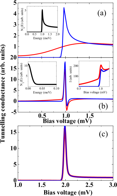
One objective of a tunneling spectroscopy imaging experiment in a superconductor is to obtain with highest precision the energy dependence of the density of states of the superconductor as a function of the position at all temperatures or magnetic fields. The tunneling current between tip and sample can be written as , and is the result of the convolution of the densities of states of tip and sample , weighted by the Fermi function [1, 21]. When the tip is made of a non superconducting metal, is energy-independent, and the differential tunneling conductance is simply smeared by the Fermi function[1, 22]. When is low enough, is practically equal to , but when increasing the temperature, the tunneling conductance may be significantly smeared (Fig.1 a), and measurement uncertainty coming from noise significantly influences the final de-convolution[23].
Consider now, for example, a tip with a function like sharp peak at the Fermi level, in an otherwise finite and energy independent density of states, such as the one produced by a localized state close to the tip[24, 25]. In that case, the I(V) curve directly reflects the density of states of the sample, with a peak at the gap edge. The conductance has correspondingly pronounced maxima and minima, and passes through zero exactly at the position of the peak in I(V). When increasing temperature, the current below the gap edge increases exponentially, reflecting the thermal behavior of the tail of the Fermi function[26], but features in at the gap edge are largely unaffected (Fig.1 b). If the density of states of the tip is well known and independent of temperature, then the de-convolultion of the sample’s density of states from the I-V curve or from the tunneling conductance remains precise when increasing temperature. Localized state features which give peak shaped densities of states have been observed in some cases close to defects or impurities[24, 25, 27, 28]. Tips with impurities located close to the apex could therefore give interesting results, although they still need to be realized in a controlled way.
A superconducting tip leads to even better results. The form and properties of the density of states of tips made of well known superconductors have been previously reported with detail[2, 29, 30, 31, 32, 33, 34, 35, 36, 37]. The quasiparticle peaks located at the gap edge lead to a sharp anomaly at the sum of the tip and sample’s superconducting gaps (Fig.1c). When increasing temperature, the width of the corresponding anomaly does not change, making the determination of the LDOS of the sample through de-convolution accurate at all temperatures [38, 39].
3 Scanning Andreev Reflection Spectroscopy with superconducting tips.
Superconducting tips also allow, on the other hand, to probe the Josephson effect at the local level[30, 40, 41], and they could enable designing, in future, local phase sensitive experiments[2, 42]. There is yet another important feature which has not been explored until now. In particular, at the lowest temperatures, the current due to thermal excitations at voltages below the superconducting gap is exponentially small. Andreev reflection between tip and sample is always present, and the corresponding current depends exponentially on the tunneling barrier[43]. Therefore, reducing the tunnel barrier at the lowest temperatures leads to the observation of a small current at bias voltages below the superconducting gap which exponentially grows when the distance between tip and sample is reduced[44]. For instance, using a superconducting tip and a normal sample, with a tunneling conductance of around some tens of S (i.e. some 0.1 G0, where G0 is the quantum of conductance), the Andreev reflection accounts for the observation of a tunneling conductance of some per cent the high voltage conductance. When scanning with a superconducting tip a superconducting sample, Andreev reflection is further suppressed, as the process requires bouncing back and forth four electronic states, instead of the two states involved in a N-S Andreev reflection process[45].
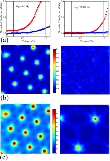
Thus, scanning with, e.g. a superconducting tip of Pb, on a sample with superconducting and normal areas, leads to a conductance at a finite voltage below the superconducting gap which changes as a function of the position, being significantly larger on top of the normal areas. Of course, the experiment needs to be made at low enough temperatures to ensure that the result does not come from thermal excitations. Moreover, local variations in the magnetic field may result in changes in the tip’s density of states which induce pair breaking effects, producing similarly a higher low bias conductance[31]. Changing the tip-sample distance is the most effective way to separate Andreev processes from other variations of the low bias voltage conductance as a function of the position. In Fig.2 we show results taken at a conductance of 17 S (left panels of Fig.2), and compare them with results taken at a conductance of 0.5 S (right panels of Fig.2), which is around 0.39% G0. While thermal excitations or pair breaking depend on the actual density of states of the tip and should be present at all tunneling tip-sample distances, Andreev reflections will decrease exponentially with distance. The left panel of Fig.2b shows the vortex lattice of NbSe2 at 0.1 T viewed by plotting as a function of the position the value of the Andreev conductance. The signature of vortices is washed out when images are taken at low tunneling conductance, below S, as shown in the right panel of Fig.2b. When the image is built from the value of the conductance at 1 mV the observed features are due to changes in the local density of states, and have been discussed previously[2, 29, 30, 31, 32, 33, 34, 35, 36]. Namely, the density of states at the center of the vortex core is high and leads to high conductance at 1mV when using a superconducting tip of Pb, and the characteristic star-shape found in NbSe2 is observed in-between vortices. This observation is independent of the value of the tunneling conductance, as is shown in Fig.2c.
This demonstrates that the localized electronic states inside the vortex cores can carry an Andreev current, which peaks at the vortex core. Note that Andreev reflection between a conventional s-wave superconductor and a metal with full spin polarization is not allowed. Thus, Scanning Andreev Spectroscopy can be developed in future as an effective tool to study local spin polarization of materials at very low temperatures.
4 Current drive scanning tunneling microscopy and spectroscopy.
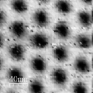
It is also important to image varying relevant thermodynamic and transport parameters, such as an applied current. Several STM/S experiments have been designed for topography measurements under an applied current. The arrangement requires to ground one side of the sample and apply a bias to the other side, with a current fixed by the resistance of the sample and the bias voltage[20, 46]. In order to study a superconductor, one requires knowledge of the full dependence. Recently, we have developed new STM/S circuitry and methods to be able to make I-V measurements as a function of the position and the current using normal tips[20]. In Fig.3 we show a vortex lattice image of NbSe2 obtained by measuring at each position a full I-V curve, and applying a current of 10 mA through the sample, at 4.2 K. Corresponding current density is of 0.4 104A/m2. Current flow can be expected to be homogeneous, because the London penetration depth is much larger than the coherence length [18]. Here we plot the normalized zero voltage conductance as a function of the position[2]. The vortex lattice is clearly viewed, so that the current is below the de-pinning value. We image therefore the pinned vortex lattice. Further measurements at lower temperatures, and as a function of the current and the magnetic field are under way.
5 Scanning tunneling microscopy and spectroscopy in a vector magnetic field.
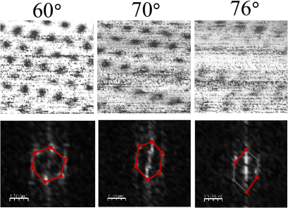
The control over the direction of the magnetic field is another important aspect which allows studying highly anisotropic samples. In particular, the vortex lattice in layered compounds is expected to show many peculiar features related to the modifications of intervortex potential when the magnetic field is turned from being perpendicular to the layers[47, 48, 49]. Recently, we have developed a dilution refrigerator three-axis vector magnet STM/S set-up, and could measure the angular dependence of the vortex lattice in NbSe2. The density of vortices decreases when the z-axis component of the magnetic field drops, following , with being the misalignment of the normal to the surface of the sample with respect to the z component of the magnetic field (here ). As observed previously in Ref.[48], the vortex lattice buckles, losing hexagonal symmetry, because it tries to orient one of the three high symmetry axis of the hexagon along the planar component of the magnetic field vector. Gradually, the hexagon is elongated and a zig-zag structure which ends up in stripe-like vortex arrangements is found. Although the vortices have been observed (Fig.4), more precise and clear measurements are needed to show this interesting feature of the tilted vortex lattice.
6 Summary and outlook.
Scanning tunneling spectroscopy has evolved as a very efficient and complete microscopy of the superconducting state. Work in superconducting tips allow to increase considerably the precision in measuring the density of states of the sample, and provides for new modes of operation. Scanning Andreev Spectroscopy (SAS) appears as an efficient way to probe Andreev reflection at the very local level, and should lead to new imaging technique sensitive to the spin polarization of the tunneling current. Further developments in measurements as a function of an applied current (CD/STS), and in a vector magnetic field, will enable new imaging possibilities. The full potential of Materials Science, with anisotropies of single crystalline materials, and of engineered Nanoscience, with phenomena related to vortex flow in different geometries and arrangement of nanostructures in superconducting samples, come into the realm of the imaging possibilities of STM/S.
References
- [1] O. Fischer, M. Kugler, I. Maggio-Aprile, C. Berthod, Scanning tunneling spectroscopy of high-temperature superconductors, Review of Modern Physics 79 (2007) 353.
- [2] J.G. Rodrigo, H. Suderow, S. Vieira, E. Bascones, F. Guinea, Superconducting nanostructures fabricated with the scanning tunnelling microscope, J. Phys.: Condens. Matter 16 (2004) R1151.
- [3] A. Abrikosov, On the Magnetic Properties of Superconductors of the Second Group, Sov. Phys. JETP 5 (1957) 1174.
- [4] G. Blatter, M.V. Feigel’man, V.B. Geshkenbein, A.I. Larkin, V.M. Vinokur, Vortices in high-temperature superconductors, Rev. Mod. Phys. 66 (1994) 1125.
- [5] E.H. Brandt, The flux-line lattice in superconductors, Rep. Prog. Phys. 58 (1995) 1465.
- [6] Nanoscience and Engineering in Superconductivity, (Eds.) V. Moshchalkov, R. Woerdenweber, W. Lang. (Springer, Berlin 2010).
- [7] T. Giamarchi, S. Bhattacharya, Vortex phases, in (Eds.) C. Berthier, L.P. Levy and G. Martinez , High Magnetic Fields: Applications in Condensed Matter Physics and Spectroscopy (Springer, Berlin 2002) p.314, cond-mat/0111052.
- [8] S.S. Banerjee, S. Goldberg, A. Soibel, Y. Myasoedov, M. Rappaport, E. Zeldov, F. de la Cruz, C.J. van der Beek, M. Konczykowski, T. Tamegai, V.M. Vinokur, Vortex Nanoliquid in High-Temperature Superconductors, Phys. Rev. Lett. 93 (2004) 097002.
- [9] I. Guillamon, H. Suderow, A. Fernandez-Pacheco, J. Sese, R. Cordoba, J.M. De Teresa, M.R. Ibarra, S. Vieira, Direct observation of melting in a two-dimensional superconducting vortex lattice, Nature Physics 5 (2009) 651.
- [10] H. Sakata, M. Oosawa, K. Matsuba, N. Nishida, H. Takeya, K. Hirata, Imaging of a Vortex Lattice in YNi2B2C by Scanning Tunneling Spectroscopy, Phys. Rev. Lett. 84 (2000) 1583.
- [11] M.R. Eskildsen, A.B. Abrahamsen, V.G. Kogan, P.L. Gammel, K. Mortensen, N.H. Andersen, P.C. Canfield, Temperature dependence of the Flux Line Lattice Transition into Square Symmetry in Superconducting LuNi2B2C, Phys. Rev. Lett. 86 (2001) 5148.
- [12] M.R. Eskildsen, K. Harada, P.L. Gammel, A.B. Abrahamsen, N.H. Andersen, G. Ernst, A.P. Ramirez, D.J. Bishop, K. Mortensen, D.G. Naugle, K.D.D. Rathnayaka, P.C. Canfield, Intertwined symmetry of the magnetic modulation and the flux-line lattice in the superconducting state of TmNi2B2C, Nature 393 (1998) 242.
- [13] I. Guillamon, M. Crespo, H. Suderow, S. Vieira, J. Brison, S.L. Bud’ko, P.C. Canfield, Atomic resolution and vortex lattice studies of magnetic superconductors: A first approach in the nickel borocarbide TmNi2B2C, Physica C 470 (2010) 771.
- [14] A.V. Silhanek, J. Van de Vondel, V.V. Moshchalkov, Guided Vortex Motion and Vortex Ratchets in Nanostructured Superconductors, in (Eds.) V. Moshchalkov, R. Woerdenweber, W. Lang., Nanoscience and Engineering in Superconductivity (Springer, Berlin 2010) p.1.
- [15] H.F. Hess, R.B. Robinson, J.V. Waszczak, Vortex-core structure observed with a scanning tunnelling microscope, Phys. Rev. Lett. 64 (1990) 2711.
- [16] N. Hayashi, T. Isoshima, M. Ichioka, K. Machida, Low-lying quasiparticle excitations around a vortex core in quantum limit, Phys. Rev. Lett. 80 (1998) 2921.
- [17] H. Nishimori, K. Uchiyama, S. Kaneko, A. Tokura, H. Takeya, K. Hirata, N. Nishida, First Observation of the Fourfold-symmetric and Quantum Regime Vortex Core in YNi2B2C by Scanning Tunneling Microscopy and Spectroscopy, J. Physs. Soc. Japan 73 (2004) 3247.
- [18] I. Guillamón, H. Suderow, F. Guinea, S. Vieira, Intrinsic atomic-scale modulations of the superconducting gap of 2H-NbSe2, Phys. Rev. B 77 (2008) 134505.
- [19] H. Suderow, I. Guillamon, S. Vieira, Compact very low temperature scanning tunneling microscope with mechanically driven horizontal linear positioning stage, Rev. Sci. Inst. 82 (2011) 033711.
- [20] A. Maldonado, I. Guillamon, H. Suderow, S. Vieira, Scanning tunneling spectroscopy under large current flow through the sample, Rev. Sci. Inst. 82 (2011) 073710.
- [21] C. Berthod, T. Giamarchi, Electron tunneling and the local density of states, arXiV:1102.3895v1.
- [22] Y.J. Song, A.F. Otte, V. Shvarts, Z. Zhao, Y. Kuk, S.R. Blankenship, A. Band, F.M. Hess, J.A. Stroscio, A 10mk scanning probe microscopy facility, Rev. Sci. Inst. 81 (2010) 121101.
- [23] M. Crespo, H. Suderow, S. Vieira, S. Bud’ko, P.C. Canfield, Local Superconducting Density of States of ErNi2B2C, Phys. Rev. Lett. 96 (2006) 027003.
- [24] A.V. Balatsky, I. Vekhter, J. Zhu, Impurity-induced states in conventional and unconventional superconductors, Rev. Mod. Phys. 78 (2006) 373.
- [25] M. Ternes, A.J. Heinrich, W. Schneider, Spectroscopic manifestations of the Kondo effect on single adatoms, J. Phys.: Condens. Matter 21 (2009) 053001.
- [26] A. Maldonado, H. Suderow, S. Vieira, Thermometry with a nearly temperature independent sensitivity using a normal-superconducting tunnel diode biased close to the superconducting gap, Cryogenics 50 (2010) 397.
- [27] A.R. Schmidt, M.H. Hamidian, P. Wahl, F. Meier, A.V. Balatsky, J.D. Garret, T.J. Williams, G.M. Luke, J.C. Davis, Imaging the Fano lattice to hidden order transition in URu2Si2, Nature 465 (2010) 570.
- [28] P.A. Aynajian, E.H. da Silva Neto, C.V. Parker, Y. Huang, A. Pasupathy, J. Mydosh, A. Yazdani, Visualizing the formation of the Kondo lattice and the hidden order in URu2Si2, Proc. Natl. Acad. Sci. USA 107 (2010) 10383.
- [29] J.G. Rodrigo, H. Suderow, S. Vieira, Superconducting nanobridges under magnetic fields, Phys. Stat. Sol. (b) 237 (2003) 386.
- [30] J.G. Rodrigo, H. Suderow, S. Vieira, On the use of STM superconducting tips at very low temperatures, Euro. Phys. J. B 40 (2004) 483.
- [31] I. Guillamón, H. Suderow, S. Vieira, P. Rodiere, Scanning tunneling spectroscopy with superconducting tips of Al, Physica C 468 (2008) 537.
- [32] H. Suderow, V. Crespo, I. Guillamon, S. Vieira, F. Servant, P. Lejay, J.P. Brison, J. Flouquet, A nodeless superconducting gap in Sr2RuO4 from tunneling spectroscopy, New Journal of Physics 11 (2009) 093004.
- [33] S.H. Pan, E.W. Hudson, J.C. Davis, Vacuum tunneling of superconducting quasiparticles from atomically sharp scanning tunneling microscope tips, Appl. Phys. Lett. 73 (1998) 2992.
- [34] O. Naaman, W. Teizer, R.C. Dynes, Fluctuation Dominated Josephson Tunneling with a Scanning Tunneling Microscope, Phys. Rev. Lett. 87 (2001) 97004.
- [35] N. Bergeal, V. Dubost, Y. Noat, W. Sacks, D. Roditchev, N. Emery, C. H?rold, J. Mareche, P. Lagrange, G. Loupias, Scanning Tunneling Spectroscopy on the Novel Superconductor CaC6, Phys. Rev. Lett. 97 (2006) 077003.
- [36] Y. Noat, T. Cren, F. Debontridder, D. Roditchev, W. Sacks, P. Toulemonde, A. San Miguel, Signatures of multigap superconductivity in tunneling spectroscopy, Phys. Rev. B 82 (2010) 014531.
- [37] H. Suderow, E. Bascones, A. Izquierdo, F. Guinea, S. Vieira, Proximity effect and strong-coupling superconductivity in nanostructures built with an STM, Phys. Rev. B 65 (2002) 100519(R).
- [38] J.G. Rodrigo, S. Vieira, STM study of multiband superconductivity in NbSe2 using a superconducting tip, Physica C 404 (2004) 306.
- [39] V. Crespo, J.G. Rodrigo, H. Suderow, S. Vieira, D.G. Hinks, I.K. Schuller, Evolution of the Local Superconducting Density of States in ErRh4B4 Close to the Ferromagnetic Transition, Phys. Rev. Lett. 102 (2009) 237002.
- [40] N. Bergeal, Y. Noat, T. Cren, Th. Proslier, V. Dubost, F. Debontridder, A. Zimmers, D. Roditchev, W. Sacks, J. Marcus, Mapping the superconducting condensate surrounding a vortex in superconducting VSi using a superconducting MgB2 tip in a scanning tunneling microscope, Phys. Rev. B 78 (2008) 140507(R).
- [41] J.G. Rodrigo, H. Suderow, S. Vieira, Scanning Tunnelling Spectroscopy of Vortices with Normal and Superconducting tips, in (Eds.) V. Moshchalkov, R. Woerdenweber, W. Lang., Nanoscience and Engineering in Superconductivity (Springer, Berlin 2010) p.257.
- [42] T. Hanaguri, Y. Kohsaka, M. Ono, M. Maltseva, P. Coleman, I. Yamada, M. Azuma, M. Takano, K. Ohishi, H. Takagi, Coherence Factors in High- Cuprate Probed by Quasi-Particle Scattering Off Vortices, Science 323 (2009) 923.
- [43] A.F. Andreev, Thermal conductivity of the intermediate state of superconductors, Sov. Phys. JETP 19 (1964) 1228.
- [44] G.E. Blonder, M. Tinkham, T.M. Klapwijk, Transition from metallic to tunneling regimes in superconducting microconstrictions: Excess current, charge imbalance, and supercurrent conversion, Phys. Rev. B 25 (1982) 4515.
- [45] M. Octavio, M. Tinkham, G.E. Blonder, T.M. Klapwijk, Subharmonic energy-gap structure in superconducting constrictions, Phys. Rev. B 27 (1983) 6739.
- [46] J.R. Kirtley, S. Washburn, M.J. Brady, Direct measurement of potential steps at grain boundaries in the presence of current flow, Phys. Rev. Lett. 60 (1988) 1546-1549.
- [47] E.H. Brandt, Tilted and curved vortices in anisotropic superconducting films, Phys. Rev. B 48 (1993) 6699.
- [48] H.F. Hess, C.A. Murray, J.V. Waszczak, Flux lattice and vortex structure in 2-NbSe2 in inclined fields, Phys. Rev. B 50 (1994) 16528.
- [49] A.I. Buzdin, A.S. Melnikov, A.V. Samokhvalov, T. Akashi, T. Matsuda, S. Tajima, H. Tadatomo, A. Tonomura, Crossover between magnetic vortex attraction and repulsion in thin films of layered superconductors, Phys. Rev. B 79 (2009) 094510.