Atomic-scale effects behind structural instabilities in Si lamellae during ion beam thinning
Abstract
The rise of nanotechnology has created an ever-increasing need to probe structures on the atomic scale, to which transmission electron microscopy has largely been the answer. Currently, the only way to efficiently thin arbitrary bulk samples into thin lamellae in preparation for this technique is to use a focused ion beam (FIB). Unfortunately, the established FIB thinning method is limited to producing samples of thickness above 20 nm. Using atomistic simulations alongside experiments, we show that this is due to effects from finite ion beam sharpness at low milling energies combined with atomic-scale effects at high energies which lead to shrinkage of the lamella. Specifically, we show that attaining thickness below 26 nm using a milling energy of 30 keV is fundamentally prevented by atomistic effects at the top edge of the lamella. Our results also explain the success of a recently proposed alternative FIB thinning method, which is free of the limitations of the conventional approach due to the absence of these physical processes.
Since atomic-scale building blocks determine functionality in nanotechnology, understanding physical processes at this scale is crucial for the discipline. One of the most important means for achieving this knowledge is aberration-corrected high-resolution transmission electron microscopy (AC-HRTEM),Rose1990 ; Haider1998 a method which allows determining the positions of atomic columns of a structure with accuracy higher than interatomic distance in solids.Jia2003 ; Zhang2009 HRTEM requires thin, unbent samples which ideally should contain no amorphous surface layer. Moreover, in nanotechnology, it is mandatory to achieve sample preparation with a sub-m precision in all dimensions. These standards cannot be reached using traditional mechanical preparation methods such as mechanical milling, and thus the focused ion beam (FIB) technique, where the sample is milled into a thin lamella through sputtering, needs to be used instead.
The current development in AC-HRTEM is to lower the voltage from the usual 200–300 kV to well below 100 kV,Meyer2011 ; Chuvilin2009 ; Suenaga2009 ; Huang2011 ; Sasaki2011 ; Kaiser2011 in order to minimize displacement damage in fragile samples.444For example, voltages below 50 kV are required to prevent displacement of atoms at graphene edges or next to vacancies.Kotakoski2012 So far, predominantly low-dimensional materials such as grapheneMeyer2011 ; Huang2011 ; Kaiser2011 , hexagonal boron nitrideChuvilin2009 , and carbon nanotubesSuenaga2009 have been studied at low electron beam voltages by HRTEM. In the future, however, there will be a demand to extend these low-voltage studies to conventional materials, which similarly suffer from knock-on damage at higher voltages. This trend of lowering voltage entails an increasingly stringent requirement for sample thickness, which must not surpass the extinction length of the electron beam (few nm). However, the conventional FIB thinning method is limited to thicknesses above 20 nm. The dominant effect behind this limitation is the shrinkage of the lamella in height during milling: Thinning a lamella down to a thickness of 20 nm may induce several m of shrinkage in the vertical direction.Kang2010 The underlying physical reasons for this observation are currently not known, because an atomic-scale description of the thinning process has hitherto not been presented. Additionally, the conventional method is hampered by specimen warping, an uneven thickness profile, and often heavy amorphization.
Although irradiation effects in Si have been studied for decades, the work has concentrated on bulk Si samples.Cha97 ; Pos00b ; Nor97f ; Ric07 Moreover, earlier computational work on FIB processing of similar nanosystems has been restricted to simulation setups which severely reduce the applicability of the obtained results to the problem addressed in the present study. On the one hand, some studies have employed less detailed models based on Monte Carlo simulation of sputtering and redeposition on a three-dimensional grid.Katardjiev1994 ; Kim2007 Unfortunately, such models lack real atomic resolution and hence do not account for, e.g., amorphization, which alone renders them powerless for the topic at hand. On the other hand, previous molecular dynamics (MD) simulations motivated by FIB milling have employed geometries restricted to a single surface with no deformation of the sample allowed,Russo2008 ; Pastewka2009 ; Giannuzzi2009 thus yielding comparatively limited insight into the process. To uncover the mechanisms responsible for the deleterious effects on the lamella under conventional FIB thinning, we performed a classical MD study of the FIB thinning process in conjunction with experiments. Using the findings from our experiments and simulations, we show that the empirically observed limit of 20 nm for the conventional thinning method is a result of geometric sputtering effects due to the finite sharpness of the ion beam, dominant at low energies (1 keV), and of atomic-scale effects at the very top part of the lamella, significant at high energies (30 keV). We further explain why these mechanisms are not present in a recently proposed double-tilt method,Lechner2011 which thus allows the thinning process to proceed beyond the conventional limit.
The experimental setup and the conventional FIB thinning method are described in Appendix A. The effect of ion beam tails, discussed below, is demonstrated in Appendix B. Here, we focus first on studying experimentally the deleterious shrinkage effect on a lamella during FIB thinning. In principle, creating a wedge-shaped lamella would show shrinkage versus thickness in a straightforward experiment. However, the structural stability of such a geometry is reduced fast during thinning, and warping of the sample occurs. Therefore, we instead thinned a co-planar Si lamella in a double-wedge configuration (Fig. 1): Material was removed from one side by milling at a horizontal tilt of 4∘ and from the other side at 1∘ but with a vertical rotation of 0.5∘. The resulting lamella thus gets gradually thinner from bottom to top and from right to left with the very thin areas restricted to the top edge to limit warping. Milling parameters for the fabrication were identical to the single-edge experiment of Appendix B. For a given material and set beam conditions the absolute thickness of the lamella can be estimated from scanning electron microscope (SEM) image contrast.Salzer:2009jq In the secondary electron SEM image of Fig. 1, the thickness gradient of the lamella manifests in a contrast gradient with the thin areas appearing lighter.
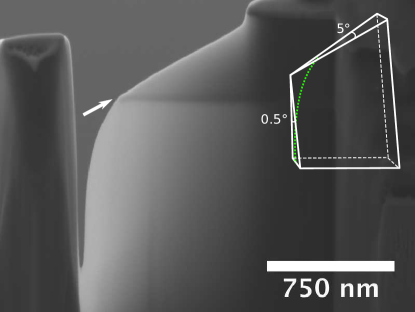
Based on purely the milling geometry, the thin top-edge of the created double-wedge lamella should be straight, as shown in the schematic illustration of Fig. 1. Instead, we observe a strongly falling edge indicating that the removal of lamella material in the vertical direction is greatly increased when the thickness drops below a certain threshold. Furthermore, very thin areas ( nm) are notably absent in the wedge lamella. In fact, we could not find any experimental conditions that would have allowed us to create a very thin Si edge using 30 keV Ga ions. We tried shortening the line dwell time/milling depth to reduce the corner rounding – to no avail. Reducing the beam current and thus sharpening the beam did not prove a viable option either since the resulting milling times were excessive, leading to problems from stage drift. Consequentially, we can unfortunately not draw any quantifiable conclusions from the thinning experiments except that we were not able to create very thin areas, and that there is a thickness-dependent vertical shrinkage effect for the thinnest parts of the structure. 555Similarly, we find that it seems not possible to create tips, e.g., from tungsten, with a radius smaller 20 nm.
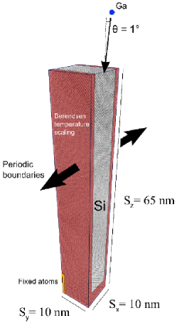
In order to understand the unexpected shrinkage of the lamella below the threshold thickness, an atomic-level description of the irradiation process is required. Our MD simulation setup, designed for studying ion irradiation effects on the top edge of a short section of a thin Si lamella, is visualized in Fig. 2. In all simulations, the studied system size was 65 nm in the vertical () direction and 10 nm in width (-direction), periodic boundaries being applied in the latter dimension to mimic a much wider lamella edge. The beam, assuming a Gaussian distribution with a standard deviation of 2.5 nm in both the and -direction, was directed at the edge of the lamella at an angle of . The thickness of the edge was controlled by the size of the system in the -direction ( nm). The simulation setup is further detailed in Appendix C, and the performed runs are described in Appendix D.
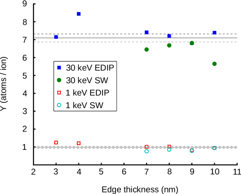
In Fig. 3, we plot sputtering yield as a function of edge thickness for 1 keV and 30 keV Ga+ irradiation as given by two different Si–Si interaction potentials (Appendix C). The data is clearly grouped by the beam energy: The thickness of the system seems to have no systematic effect on the results. On average, the 30 keV beam produces a of atoms/ion, whereas the 1 keV beam gives atoms/ion, as averaged over all system sizes and potentials. To better understand whether the irradiation energy leads to other differences beyond those in during the milling, we carried out an extensive analysis of different physical effects occuring during the process. For all simulated cases, the initial positions of sputtered atoms were determined after each irradiation event. Secondly, the center of mass of the system in the -direction was calculated as a function of the -coordinate. Thirdly, the degree of amorphization of each system was determined likewise as a function of using structure factor analysis.Nor96d
Our analysis shows that the 1 keV beam results in the smoothening of the initially abrupt upper corner of the edge, which would lead to milling of the edge upon continued irradiation. The corner is amorphized, and sputtering is mainly from the impact region. However, the effect of the 30 keV beam, as presented in Fig. 4, is more interesting. At this beam energy, the 7 nm structures bend toward the edge onto which the beam is aimed. This is verified by the diagrams showing the center of mass in the -direction as a function of the edge height, which clearly reflect what is seen in the snapshot of the final state of each system. Also, the apparent amorphization seen in the snapshots is confirmed by the quantitative amorphization analysis. Sputtering is induced over the entire front face of the system and somewhat at the back face also. For edges 7 nm, however, almost no bending is observed at the dose of 500 ions. Instead, the system simply shrinks vertically as a result of the ion bombardment. Correspondingly, sputtering for the thinnest structures is no longer predominantly off the front face but also significant off the back of the structure.
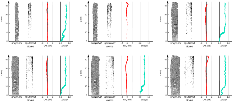
Based on the results presented above, it would seem that the 30 keV beam induces mainly bending and modest shrinking in the thicker edges (7 nm) and predominantly shrinking in the thinnest edges. This inference is supported by studying the evolution of the atomic structure of the 10 and 3 nm edges as a function of the 30 keV irradiation dose, as presented in Figs 5(a,b), respectively. As the dose increases, the 10 nm system bends toward the corner where the beam is incident, whereas the 3 nm system shrinks by nearly 10 nm in height as the dose is brought to 1000 ions. The explanation for these two distinct modes of behavior can be found by considering the positions of sputtered atoms in each case and taking into account the resulting surface tension. As noted above and as seen in Fig. 4, sputtering for the 7 nm edges occurs mainly off the front face of the structure. Therefore, the system will relax, i.e., minimize its free energy to a local minimum, by contracting the front face in the vertical dimension, hence pulling the structure into a forward-bent position. Correspondingly, when atoms are sputtered evenly off both the front and back faces, as for the 7 nm edges, the bending behavior is taken over by the shrinkage of the system in the vertical direction, as the structure relaxes by contracting along the entire thickness.
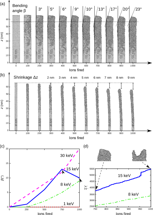
Note that the above-described bending is not the same phenomenon as the deleterious warping observed experimentally in the sample during conventional FIB thinning. The empirical warping happens in the opposite direction relative to the beam, and throughout the bulk of the lamella. Perhaps counterintuitively, the bending as described by our simulations will actually appear as shrinkage of the lamella top in the experiments. This is because the tilted structure is etched away more efficiently by the incoming ions than the originally straight-standing one. Obviously, this erosion process is very difficult to observe experimentally, and has therefore not been detected before. One example of how the erosion might proceed is presented below in Fig. 5(d). Here a large density of deposited energy on the top of the bent structure causes hundreds of atoms to sputter with a single ion hit and leads to the subsequent straightening of the lamella edge. For the extreme case of lamella edges 7 nm, sputtering from both the front and back faces simply constitutes another mechanism of shrinkage.
Focusing on the described bending of the edge in more detail, it can be seen in Fig. 5(c) that an 8 keV ion beam is energetic enough to induce bending in the 10 nm structure, whereas at 1 keV the edge is left standing upright. Looking at the bent structures in Figs 4 and 5(a), it can be discerned that the top part of the bent structure is as if bent around a hinge at a well-defined height on the back face of the structure, as illustrated explicitly by the horizontal line in Fig. 5(a). This point is roughly around the area where the amorphization starting from the front face of the structure reaches the back face, which is where the originally rigid crystalline back wall gives way to the contracting force on the front face of the system. Such a mechanism is functional only when the system is thin enough to allow for the amorphization to proceed all the way through the structure. For sufficiently thick structures this does not happen. We emphasize that this does not require a complete amorphization of the structure. Instead, it is enough if the damage reaches the back face at one location. This may happen outside the collision cascade, as was shown recently.Pothier2011
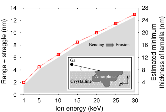
To predict the minimum attainable thickness of the lamella top edge according to this erosion mechanism, we performed a set of SRIM runs with Ga+ incident on a Si target at an angle of at energies from 1 to 30 keV. To quantify the effect of the ions in the -direction, we calculated the sum of ion range and straggle for the different energies (Fig. 6). To first assess how these results compare with MD data, we noted that for the 10 nm thick edge, the thickness of the amorphous layer in our MD simulations in the -direction is 3 to 5 nm for 1 keV ions, and for 8 keV ions the thickness already surpasses 10 nm. A comparison of these two points to the SRIM results in Fig. 6 shows that the SRIM results give roughly half the thickness of the amorphous layer. The difference is due to the fact that in the SRIM calculations only ions incident on the front face of the structure are included, whereas in the MD runs, ions incident on the very top of the structure are simulated as well. Another factor possibly contributing to this discrepancy is a recently predicted damage flow mechanism in amorphous Si.Pothier2011 Taking into account this factor of two difference leads to the prediction that at 30 keV, lamella edges of thicknesses 26 nm will be subjected to bending into the beam and hence catastrophic erosion. This explains why very thin lamella edges were completely absent in our experiments using the 30 keV Ga ion beam.
Regarding the warping seen in the experiment, the likely explanation for the phenomenon is to be found from previous studies of Si wafer curvature as brought on by ion implantation:Volkert91 As the FIB is used to mill the face of the lamella, the surface region is amorphized, which causes the region to expand and hence to bend the lamella in the observed manner. The relevant scale for the effect is much larger than that in the present MD simulations. Furthermore, the mechanism relying on surface tension producing the bending toward the beam is dominant in our study over volume changes due to amorphization. The volume change of Si upon amorphization is predicted to be positive (as in experiment) for EDIP and negative for SW,Nord02 but nevertheless both potentials reproduce the bending of the top part of the lamella edge in the same direction. In our simulations, this is due to the small size of the structures; the smaller a system is, the higher its surface area to volume ratio, and hence any surface effects are pronounced in smaller systems.
In conclusion, we have experimentally demonstrated the well-known fact that a FIB milling energy of 30 keV cannot be used to create very thin lamellae ( nm) within the conventional thinning approach. Our simulations reveal that this limitation is a fundamental one, being due to atomic-scale effects at the top edge of the lamella which lead to the erosion of the structure under the ion beam. Specifically, we predict that an edge of thickness 26 nm will be subject to catastrophic erosion through the lamella top edge bending into the beam. This effect can be reduced by lowering the beam energy, but the lower the energy, the more significant the effects of the beam tails become (Appendix B). Together these two mechanisms of shrinkage lead to the lower limit of nm for the thickness of the lamella during conventional FIB thinning. Our results explain why the alternative double-tilt approach (Appendix E) is free of these harmful effects, and can be used for preparing extremely thin samples of good quality for current and future AC-HRTEM studies.
ACKNOWLEDGEMENTS
The theoretical research for this study was supported by the Academy of Finland Center of Excellence in Computational Molecular Science and the Helsinki Institute of Physics. EH is grateful to Michael Moseler and Karsten Albe for valuable comments. Generous grants of computer time from the Center for Scientific Computing in Espoo, Finland are thankfully acknowledged. The experimental research was funded by the German Research Foundation (DFG) and the State of Baden-Württemberg through the SALVE (Sub-Ångström Low-Voltage Electron Microscopy) project.
APPENDIX A: CONVENTIONAL FIB THINNING METHOD
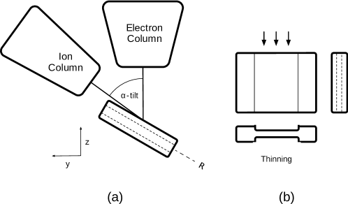
Throughout the study, sample fabrication was performed in a Zeiss NVision 40 CrossBeam FIB instrument incorporating a Ga liquid metal ion source and in-situ scanning electron microscopy (SEM) imaging using a thermal field emission source. The energy of the Ga ions can be varied in the range from 1 to 30 keV. Figure 7(a) shows a schematic drawing of the microscope. TEM lamella preparation by the FIB lift-out method is carried out in four steps:Langford:2004ea (1) Rough milling of a lamella, (2) lift-out, (3) thinning, and (4) polishing. During rough milling, a free-standing structure containing the region of interest is created by removing material around it through FIB milling. Then, for lift-out, a manipulator is attached to the structure using ion beam induced deposition (IBID). Subsequently, the structure is cut free from the bulk. Using the manipulator, the resulting lamella is transferred to a special TEM lift-out grid. Once it is firmly attached by IBID it can be thinned further using high energy ion beam milling. In order to reduce the resulting damage layer (30 nm for 30 keV Ga ions in Si) the Ga ion energy is reduced for one or more polishing step(s). Figure 7(b) shows a schematic drawing of the lamella during the thinning and polishing process of the conventional in-situ lift-out technique. The lamella faces are milled under a glancing angle of 1 to 3∘ (depending on milling current) to obtain co-planar surfaces. In conventional thinning, material is removed top–down from one or both sides of the lamella. Polishing is done analogously, until the desired final thickness is reached.
APPENDIX B: SPUTTERING GEOMETRY
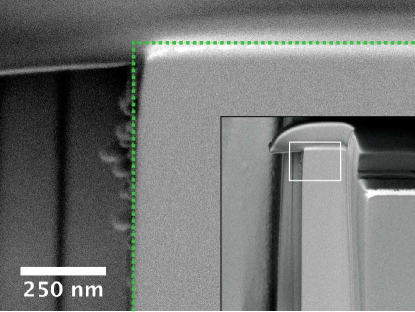
In order to understand the different effects leading to the shrinking behavior of the lamella in the conventional FIB method, we studied the sputtering geometry resulting from finite beam sharpness effects on a single edge. Fig. 8 shows an SEM image of the cross-section through a FIB-prepared thick Si lamella. The sidewalls of the lamella were milled using a 30 kV Ga ion beam with a current of 10 pA at 1∘ incidence angle. The beam diameter (FWHM) was 20 nm and the milling depth was set to 10 m. The beam was repeatedly scanned quickly on the same line until the desired milling depth was reached. The resulting edge is perpendicular to the sample surface but with a rounded top. As seen in the figure, the rounding effect is already in the 10 nm range at a beam voltage of 30 kV, and should become much worse at lower voltages due to chromatic lens aberrations.
APPENDIX C: SIMULATION METHOD
As obtaining an atomic-level description of the FIB thinning process involves following the time evolution of hundreds of thousands of atoms for thousands of time steps for each ion impact event, MD simulation with analytical interatomic potentials, which also provides a reasonably accurate atomistic description, is currently the only feasible method for the investigation. In addition to MD, we carried out a set of calculations within the binary collision approximation scheme as implemented in the SRIM code.SRIM-2008 ; SRIMbook These simulations were performed in order to get an estimate of how some of our MD results could be extrapolated to larger system sizes utilizing the simpler physical model of SRIM, as explained above.
Arguably, the most critical part in designing an MD simulation is selecting the interaction model. For Si, more than 30 analytical potentials have been published.Baz97 Out of these, the most common and well-established potentials for studying radiation damage are the Stillinger-Weber (SW),SW , Tersoff (TS),Ter88c , and Environment-Dependent Interatomic Potential (EDIP).Jus98 Regarding irradiation effects, the displacement threshold energy and the sputtering yield can be considered to be the decisive properties in describing the relevant processes. Unfortunately, all of the three mentioned potentials have been shown to underestimate as compared to density-functional theory calculations.Holmstrom09 SW produces the highest average of 29 eV, whereas EDIP gives the lowest value of 16 eV. TS falls between these two extremes with 19 eV. The DFT value is as high as 35–36 eV. Additionally, given by EDIP has been shown to give the closest match with experiment for Ar ions with energies up to 20 keV,Samela2007 whereas SW and TS agree well with each other but somewhat underestimate the experimental results. Thus, as SW gives the best value for , whereas EDIP describes sputtering in best accordance with experiments, we started our simulations using EDIP and SW in parallel. However, it turned out that there were no significant differences in the results between these two potentials, and hence the work was completed using EDIP.
For modeling the Ga–Si interaction, a purely repulsive ZBL potential ZBL was used, because the Coulombic interaction between the nuclei is the overwhelmingly dominating effect in high-energy collisions, and the finer chemistry between the two types of atoms can be neglected. Indeed, chemical effects should affect irradiation results only when the projectile energy is very low ( 100 eV).Ahlgren2011 We have previously used a similar approach to model Ga impacts on graphene in the keV energy range.Lehtinen2011 To realistically model high-energy Si–Si collisions brought on by the up to 30 keV ion impacts, a separate ZBL high-energy part was smoothly splined to the repulsive part of the Si–Si potentials at small interatomic distances.Nor94 Finally, to account for electronic stopping of energetic atoms, a frictional, velocity-dependent drag force was applied to all atoms with a kinetic energy higher than 5 eV.
To model the dissipation of energy deposited into the irradiated structure by an incident ion, the system was coupled to a Berendsen thermostat Ber84 at a temperature of 10 K with a time constant of 300 fs in a region with a thickness of 0.8 nm at the periodic boundaries and 1.5 nm from the bottom of the structure. As those parts of the system which are coupled to the thermostat constitute an effective boundary in the periodic -direction, the system was translated over the periodic boundaries for each ion impact event so that the impact point in the -direction was always halfway between the regions where temperature was being scaled. Also, to prevent the entire structure from moving as a result of the ion impacts, a small segment encompassing 3000 atoms in the lower back face of the system was fixed. Each ion impact simulation was carried out for 15 ps, which was enough to model the ballistic phase of the irradiation event. After this, the temperature of the system was slowly decreased to the initial simulation temperature of 10 K before the next impact. All simulations were performed using the parcas MD code.PARCAS
APPENDIX D: SIMULATION RUNS
The first set of runs consisted of simulating edges of thicknesses 3–10 nm. 66610 nm is the maximum thickness that could be modeled with our approach in a reasonable computation time. In order to simultaneously study both the role of thickness and that of beam energy, we carried out these simulations for irradiation energies of 1 keV and 30 keV up to a total beam dose of 500 ions. We also performed the same set of runs using a beam energy of 500 eV, but found no noteworthy differences to the 1 keV case.
Due to the differences observed for the 1 keV and 30 keV irradiations (as described above), we performed another set of simulations to investigate intermediate energies. These complementary runs with beam energies of 8 and 15 keV were performed on the 10 nm edge. To make sure we weren’t missing any important effects due to too low a dose, we at this point increased the total dose to 1000 ions. Finally, we extended the earlier simulations for the 3 and 10 nm edges up to this same dose. It is worth noting that even these ’high’ doses are far from the experimental ones. However, the simulations therefore allow us to detect effects which may disappear too fast in the experiment to be directly observed.
APPENDIX E: ATTAINING THE THINNEST POSSIBLE LAMELLA
It has always been best practice to reduce the ion beam energy as the lamella becomes progressively thinner. After all, the goal of TEM sample preparation is to retain as much pristine material as possible inside the lamella. Despite this, no ultra-thin lamellae have been produced using the conventional method. The problem ultimately lies in the dominating effect of chromatic lens aberrations at low acceleration voltages which significantly increase the beam diameter. During thinning and polishing, the resulting wide beam tails result in the rounding of the edges of the lamella top. When a lamella is thinned from both sides, these tails may overlap causing shrinkage. Besides shrinkage, these tails cause the top edge to become significantly thinner than the rest of the lamella. This thin edge is eroded away through bending into the beam and sputtering from both sides, as described above by our simulations. Reducing the beam energy further does decrease these top edge effects (as seen in Fig. 6), but in turn also increases geometric shrinking of the bulk of the lamella. The resulting trade-off seems to set a fundamental lower limit of 20 nm to lamella thickness attainable using the conventional thinning method.
However it was shown recently that the conventional limit can be overcome using the double-tilt method.Lechner2011 Within this approach, the detrimental formation of a sharp edge during thinning is omitted by milling perpendicular grooves in the front and the back sides of the sample. The thin transparent area of the lamella is formed where the grooves overlap. Geometric and top edge effects are thus effectively suppressed since there is no free edge, independent of the lamella’s final thickness. In addition, amorphization of the lamella surface can be reduced to a minimum since no trade-off between beam energy, milling angle, and tolerable focus spread has to be made. Even low-kV Ar ion polishing, typically featuring beam diameters of 10 to 100 m, can be performed at grazing incidence. Last but not least, the mechanical stability of the resulting lamella is much higher than that obtained with the conventional method since the transparent window is surrounded on all sides by a thick frame of material. These points explain why the double-tilt method can be used to obtain results superior to those of the conventional method.
References
- (1) H. Rose, Optik 85, 19 (1990).
- (2) M. Haider, S. Uhlemann, E. Schwan, H. Rose, B. Kabius, and K. Urban, Nature 392, 768 (1998).
- (3) C. L. Jia, M. Lentzen, and K. Urban, Science 299, 870 (2003).
- (4) Z. Zhang and U. Kaiser, Ultramicroscopy 109, 1114 (2009).
- (5) J. C. Meyer, S. Kurasch, H.-J. Park, V. Skakalova, D. Künzel, A. Groß, A. Chuvilin, G. Algara-Siller, S. Roth, T. Iwasaki, U. Starke, J. H. Smet, and U. Kaiser, Nature Materials 10, 209 (2011).
- (6) A. Chuvilin, J. C. Meyer, G. Algara-Siller, and U. Kaiser, New Journal of Physics 11, 083019 (2009).
- (7) K. Suenaga, Y. Sato, Z. Liu, H. Kataura, T. Okazaki, K. Kimoto, H. Sawada, T. Sasaki, K. Omoto, T. Tomita, T. Kaneyama, and Y. Kondo, Nature Chemistry 1, 415 (2009).
- (8) P. Y. Huang, C. S. Ruiz-Vargas, A. M. van Der Zande, W. S. Whitney, M. P. Levendorf, J. W. Kevek, S. Garg, J. S. Alden, C. J. Hustedt, Y. Zhu, J. Park, P. L. McEuen, and D. A. Muller, Nature 469, 389 (2011).
- (9) T. Sasaki, H. Sawada, F. Hosokawa, Y. Shimizu, T. Nakamichi, S. Yuasa, M. Kawazoe, T. Kaneyama, and Y. Kondo, Microsc. Microanal. 17, 1530 (2011).
- (10) U. Kaiser, J. Biskupek, J. C. Meyer, J. Leschner, L. Lechner, H. Rose, M. Stöger-Pollach, A. N. Khlobystov, P. Hartel, H. Müller, M. Haider, S. Eyhusen, and G. Benner, Ultramicroscopy 111, 1239 (2011).
- (11) For example, voltages below 50 kV are required to prevent displacement of atoms at graphene edges or next to vacancies.Kotakoski2012 .
- (12) H.-J. Kang, J. H. Kim, J. W. Oh, T. S. Back, and H. J. Kim, Microscopy and Microanalysis 16, 170 (2010).
- (13) E. Chason, S. T. Picraux, M. Poate, J. O. Borland, M. I. Current, T. Diaz de la Rubia, D. J. Eaglesham, O. W. Holland, M. E. Law, C. W. Magee, J. W. Mayer, J. Melngailis, and A. F. Tasch, J. Appl. Phys 81, 6513 (1997).
- (14) M. Posselt, Mater. Sci. Semicond. Process. 3, 317 (2000).
- (15) K. Nordlund, M. Ghaly, R. S. Averback, M. Caturla, T. Diaz de la Rubia, and J. Tarus, Phys. Rev. B 57, 7556 (1998).
- (16) M.-I. Richard, T. H. Metzger, V. Holy, and K. Nordlund, Phys. Rev. Lett. 99, 225504 (2007).
- (17) I. V. Katardjiev, G. Carter, M. J. Nobes, S. Berg, and H.-O. Blom, J. Vac. Sci. Tech. A 12, 61 (1994).
- (18) H.-B. Kim, G. Hobler, A. Steiger, A. Lugstein, and E. Bertagnolli, Nanotech. 18, 145303 (2007).
- (19) M. F. Russo, M. Maazouz, L. A. Giannuzzi, C. Chandler, M. Utlaut, and B. J. Garrison, Appl. Surf. Sci. 255, 828 (2008).
- (20) L. Pastewka, R. Salzer, A. Graff, F. Altmann, and M. Moseler, Nucl. Inst. Meth. Phys. Res. B. 267, 3072 (2009).
- (21) L. A. Giannuzzi and B. J. Garrison, J. Vac. Sci. Tech. A 25, 1417 (2007).
- (22) L. Lechner, J. Biskupek, and U. Kaiser, Microsc. Microanal. 17, 628 (2011).
- (23) R. Salzer, A. Graff, M. Simon, and F. Altmann, in Microscopy and Microanalysis (Cambridge University Press, 2009) pp. 340–341.
- (24) Similarly, we find that it seems not possible to create tips, e.g., from tungsten, with a radius smaller 20 nm.
- (25) A. Stukowski, Modelling Simul. Mater. Sci. Eng. 18, 015012 (2010).
- (26) K. Nordlund and R. S. Averback, Phys. Rev. B 56, 2421 (1997).
- (27) J.-C. Pothier, F. Schiettekatte, and L. J. Lewis, Phys. Rev. B 83, 235206 (2011).
- (28) C. A. Volkert, J. Appl. Phys. 70, 3521 (1991).
- (29) J. Nord, K. Nordlund, and J. Keinonen, Phys. Rev. B 65, 165329 (2002).
- (30) R. Langford and C. Clinton, Micron 35, 607 (Oct. 2004).
- (31) J. F. Ziegler, SRIM-2008 software package, available online at http://www.srim.org.
- (32) J. F. Ziegler, J. P. Biersack, and M. D. Ziegler, SRIM - The Stopping and Range of Ions in Matter (SRIM Co., Chester, Maryland, USA, 2008).
- (33) M. Z. Bazant, E. Kaxiras, and J. F. Justo, Phys. Rev. B 56, 8542 (1997).
- (34) F. A. Stillinger and T. A. Weber, Phys. Rev. B 31, 5262 (1985).
- (35) J. Tersoff, Phys. Rev. B 38, 9902 (1988).
- (36) J. F. Justo, M. Z. Bazant, E. Kaxiras, V. V. Bulatov, and S. Yip, Phys. Rev. B 58, 2539 (1998).
- (37) E. Holmström, A. V. Krasheninnikov, and K. Nordlund, in Ion Beams and Nano-Engineering, MRS Symposium Proceedings, Vol. 1181, edited by D. Ila, J. K. N. Lindner, P. K. Chu, J. Baglin, and N. Kishimoto (MRS, Warrendale, PA, USA, 2009) pp. DD05–02.
- (38) J. Samela, K. Nordlund, J. Keinonen, and V. N. Popok, Nucl. Instr. Meth. Phys. Res. B 255, 253 (2007).
- (39) J. F. Ziegler, J. P. Biersack, and U. Littmark, The Stopping and Range of Ions in Matter (Pergamon, New York, 1985).
- (40) E. H. Åhlgren, J. Kotakoski, and A. V. Krasheninnikov, Phys. Rev. B 83, 115424 (2011).
- (41) O. Lehtinen, J. Kotakoski, A. V. Krasheninnikov, and J. Keinonen, Nanotech. 22, 175306 (2011).
- (42) K. Nordlund, J. Keinonen, and A. Kuronen, Physica Scripta T54, 34 (1994).
- (43) H. J. C. Berendsen, J. P. M. Postma, W. F. van Gunsteren, A. DiNola, and J. R. Haak, J. Chem. Phys. 81, 3684 (1984).
- (44) K. Nordlund(2006), parcas computer code. The main principles of the molecular dynamics algorithms are presented in Nor97f ; Gha97 . The adaptive time step and electronic stopping algorithms are the same as in Nor94b .
- (45) 10 nm is the maximum thickness that could be modeled with our approach in a reasonable computation time.
- (46) J. Kotakoski, D. Santos-Cottin, and A. V. Krasheninnikov, ACS Nano 6, 671 (2012).
- (47) M. Ghaly, K. Nordlund, and R. S. Averback, Phil. Mag. A 79, 795 (1999).
- (48) K. Nordlund, Comput. Mater. Sci. 3, 448 (1995).