Ferrite cavities
Abstract
Ferrite cavities are used in synchrotrons and storage rings if the maximum RF frequency is in the order of a few MHz. We present a simple model for describing ferrite cavities. The most important parameters are defined, and the material properties are discussed. Several practical aspects are summarized, and the GSI SIS18 ferrite cavity is presented as an example.
0.1 Introduction
The revolution frequency of charged particles in synchrotrons or storage rings is usually lower than . Even if we consider comparatively small synchrotrons (e.g., HIT/HICAT in Heidelberg, Germany, or CNAO in Pavia, Italy, of about diameter, both used for tumour therapy), the revolution time will be greater than since the particles cannot reach the speed of light. Since, according to
the RF frequency is an integer multiple of the revolution frequency, the RF frequency will typically be lower than if only small harmonic numbers are desired. For such an operating frequency, the spatial dimensions of a conventional RF resonator would be far too large to be used in a synchrotron. One way to solve this problem is to reduce the wavelength by filling the cavity with magnetic material. This is the basic idea of ferrite-loaded cavities [1]. Furthermore, this type of cavity offers a simple means to modify the resonant frequency in a wide range (typically up to a factor of ) and in a comparatively short time (typically at least cycle time). Therefore, ferrite cavities are suitable for ramped operation in a synchrotron.
Owing to the low operating frequencies, the transit-time factor of traditional ferrite-loaded cavities is almost and therefore not of interest.
0.2 Permeability of magnetic materials
In this article, all calculations are based on permeability quantities for which
holds. In material specifications, the relative permeability is given which means that we have to multiply with to obtain . This comment is also valid for the incremental/differential permeability introduced in the following.
In RF cavities, only so-called soft magnetic materials which have a narrow hysteresis loop are of interest since their losses are comparatively low (in contrast to hard magnetic materials which are used for permanent magnets111No strict separation exists between hard and soft magnetic materials.).
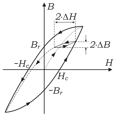
Figure 1 shows the hysteresis loop of a ferromagnetic material. It is well known that the hysteresis loop leads to a residual induction if no magnetizing field is present and that some coercive magnetizing field is needed to set the induction to zero.
Let us now assume that some cycles of the large hysteresis loop have already passed and that is currently increasing. We now stop increasing the magnetizing field in the upper right part of the diagram. Then, is decreased by a much smaller amount , afterwards increased again by that amount , and so forth222The factor of was assumed in order to have the same total change of as in the equation which is usually used for harmonic oscillations.. As the diagram shows, this procedure will lead to a much smaller hysteresis loop where changes by . We may therefore define a differential or incremental permeability333In a strict sense, the differential permeability is the limit for .
which describes the slope of the local hysteresis loop. It is this quantity which is relevant for RF applications. One can see that can be decreased by increasing the DC component of . Since is generated by currents, one speaks of a bias current that is applied in order to shift the operating point to higher inductions leading to a lower differential permeability .
If no biasing is applied, the maximum is obtained which is typically in the order of a few hundred or a few thousand times .
The hysteresis loop and the AC permeability of ferromagnetic materials can be described in a phenomenological way by the so-called Preisach model which is explained in the literature (cf. [2]). Unfortunately, the material properties are even more complicated since they are also frequency-dependent. One usually uses the complex permeability
| (1) |
in order to describe losses (hysteresis loss, eddy current loss and residual loss). The parameters and are frequency-dependent. In the following, we will assume that the complex permeability describes the material behaviour in rapidly alternating fields as does the above-mentioned real quantity when a biasing field is present. However, we will omit the index for the sake of simplicity.
0.3 Magnetostatic analysis of a ferrite cavity
Figure 2 shows the main elements of a ferrite-loaded cavity. The beam pipe is interrupted by a ceramic gap. This gap ensures that the beam pipe may still be evacuated but it allows a voltage to be induced in longitudinal direction. Several magnetic ring cores are mounted in a concentric way around the beam and beam pipe (five ring cores are drawn here as an example). The whole cavity is surrounded by a metallic housing which is connected to the beam pipe.
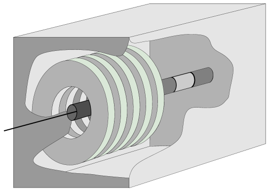
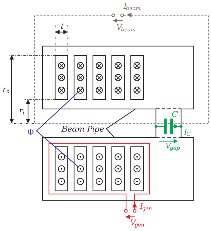
Figure 3 shows a cross-section through the cavity. The dotted line represents the beam which is located in the middle of a metallic beam pipe (for analysing the influence of the beam current, this dotted line is regarded as a part of a circuit that closes outside the cavity, but this is not relevant for understanding the basic operation principle). The ceramic gap has a parasitic capacitance, but additional lumped-element capacitors are usually connected in parallel — leading to the overall capacitance . Starting at the generator port located at the bottom of the figure, an inductive coupling loop surrounds the ring core stack. This loop was not shown in Fig. 2.
Note that due to the cross-section approach, we get a wire model of the cavity with two wires representing the cavity housing. This is sufficient for the practical analysis, but one should remember that the currents are distributed in reality.
All voltages, currents, field, and flux quantities used in the following are phasors, i.e., complex amplitudes/peak values for a given frequency .
Let us consider a contour which surrounds the lower left ring core stack. Based on Maxwell’s second equation in the time domain (Faraday’s law)
we find
| (2) |
in the frequency domain. If we now use the complete lower cavity half as integration path, one obtains
Hence we find
| (3) |
Here we assumed that the stray field in the air region is negligible in comparison with the field inside the ring cores (due to their high permeability). Finally, we consider the beam current contour:
For negligible displacement current we have Maxwell’s first equation (Ampère’s law)
We use a concentric circle with radius around the beam as integration path:
| (4) |
This leads to
| (5) |
with
| (6) |
For the flux through one single ring core we get
With the complex permeability
and assuming that ring cores are present, one finds
Therefore we obtain
| (7) |
if
| (8) |
| (9) |
are defined. Here,
| (10) |
is the quality factor (or Q factor) of the ring core material. Using Eq. (6) we find
| (11) |
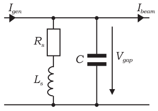
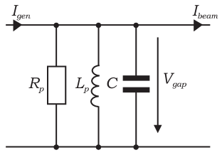
This equation corresponds to the equivalent circuit shown in Fig. 5. In the last step we defined
In the literature one often finds a different version of Eq. (11) where has the same sign as . This corresponds to both currents having the same direction (flowing into the circuits in Figs. 5 and 5). In any case, one has to make sure that the correct phase between beam current and gap voltage is established.
0.4 Parallel and series lumped element circuit
In the vicinity of the resonant frequency, it is possible to convert the lumped element circuit shown in Fig. 5 into a parallel circuit as shown in Fig. 5. The admittance of both circuits shall be equal:
A comparison of real and imaginary part yields:
(12) (13)
For the inverse relation, we modify the first equation according to
and use this result in the second equation:
Equations (12) and (13) directly provide
| (14) |
which leads to
Since it is suitable to use both types of lumped element circuit, it is also convenient to define the complex in a parallel form:
| (15) |
This is an alternative representation for the series form shown in Eq. (1) which leads to
Comparing the real and imaginary parts of the last two equations, we find:
| (16) |
| (17) |
These two equations lead to
Together with Eqs. (9), (10), and (14) we conclude:
| (18) |
With these expressions, we may write Eqs. (16) and (17) in the form
| (19) |
| (20) |
If we use Eq. (18)
we may rewrite Eqs. (12) and (13) in the form
(21) (22)
By combining Eqs. (21) and (9) we find
With the help of Eqs. (18) and (19) one gets
The last two equations lead to
This shows that is proportional to the product which is a material property. The other parameters refer to the geometry. Therefore, the manufacturers of ferrite cores sometimes specify the product (for the sake of simplicity, we define ).
For , we may use the approximations
which then have an error of less than .
0.5 Frequency dependence of material properties
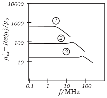
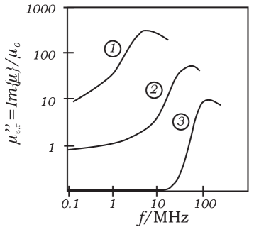
As an example, the frequency dependence of the permeability is shown in Figs. 7 and 7 for the special ferrite material Ferroxcube 4 assuming small magnetic RF fields without biasing. All the data presented for this material are taken from Ref. [3]. It is obvious that the behaviour depends significantly on the choice of the material. Without biasing, a constant may only be assumed up to a certain frequency (see Fig. 7). Increasing the frequency from upwards, the Q factor will decrease (compare Figs. 7 and 7). Figure 8 shows the resulting frequency dependence of the product.
If the magnetic RF field is increased, both and will decrease in comparison with the diagrams in Figs. 7 to 8. The effective incremental permeability will increase for rising magnetic RF fields as one can see by interpreting Fig. 1. Therefore, it is important to consider the material properties under realistic operating conditions (the maximum RF B-field is usually in the order of ).
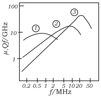
If biasing is applied, the curve shown in Fig. 8 will be shifted to the lower right side; this effect may approximately compensate the increase of with frequency [3]. Therefore, the product may sometimes approximately be regarded as a constant if biasing is used to keep the cavity at resonance for all frequencies under consideration.
0.6 Quality factor of the cavity
The quality factor of the equivalent circuit shown in Fig. 5 is obtained if the resonant (angular) frequency
is inserted into Eq. (18):
In general, all parameters , , , , , , , , and are frequency-dependent. It depends on the material whether the parallel or the series lumped element circuit is the better representation in the sense that its parameters may be regarded as approximately constant in the relevant operating range. In the following, we will use the parallel representation.
We briefly show that is in fact the quality factor defined by
where is the stored energy and is the power loss (both time-averaged):
| (23) |
At resonance, we have which leads to
as expected. The parallel resistor defined by Eq. (23) is often called shunt impedance.
0.7 Impedance of the cavity
The impedance of the cavity
may be written as
The Laplace transformation yields
which may be found in the literature in the form
if
is defined.
0.8 Length of the cavity
In the previous sections, we assumed that the ferrite ring cores can be regarded as lumped-element inductors and resistors. This is of course only true if the cavity is short in comparison with the wavelength.
As an alternative to the transformer model introduced above, one may therefore use a coaxial transmission line model. For example, the section of the cavity that is located on the left side of the ceramic gap in Fig. 3 may be interpreted as a coaxial line that is homogeneous in longitudinal direction and that has a short-circuit at the left end. The cross section consists of the magnetic material of the ring cores, air between the ring cores and the beam pipe, and air between the ring cores and the cavity housing. This is of course an idealization since cooling disks, conductors and other air regions are neglected. Taking the SIS18 cavity at GSI as an example, the ring cores have at an operating frequency of . The ring cores have a relative dielectric constant of , but this is reduced to an effective value of since the ring cores do not fill the full cavity cross section. These values lead to a wavelength of . Since 64 ring cores with a thickness of are used, the effective length of the magnetic material is (which corresponds to a phase of ). In this case, the transmission line model leads to deviations of less than 10% with respect to the lumped-element model. The transmission line model also shows that the above-mentioned estimation for the wavelength is too pessimistic; it leads to which corresponds to a cavity length of only .
This type of model makes it understandable why the ferrite cavity is sometimes referred to as a shortened quarter-wavelength resonator.
Of course, one may also use more detailed models where subsections of the cavity are modeled as lumped elements. In this case, computer simulations can be performed to calculate the overall impedance. In case one is interested in resonances which may occur at higher operating frequencies, one should perform full electromagnetic simulations.
In any case, one should always remember that some parameters are difficult to determine, especially the permeability of the ring core material under different operating conditions. This uncertainty may lead to larger errors than simplifications of the model. Measurements of full-size ring cores in the requested operating range are inevitable when a new cavity is developed. Also parameter tolerances due to the manufacturing process have to be taken into account.
In general, one should note that the total length and the dimensions of the cross-section of the ferrite cavity are not determined by the wavelength as for a conventional RF cavity. For example, the SIS18 ferrite cavity has a length of flange-to-flange although only are filled with magnetic material. This provides space for the ceramic gap, the cooling disks, and further devices like the bias current bars. In order to avoid resonances at higher frequencies, one should not waste too much space, but there is no exact size of the cavity housing that results from the electromagnetic analysis.
0.9 Cavity filling time
The equivalent circuit shown in Fig. 5 was derived in the frequency domain. As long as no parasitic resonances occur, this equivalent circuit may be generalized. Therefore, we may also analyse it in the time domain (allowing slow changes of with time):
| (24) |
| (25) |
Here we used the definition
The product is also present in the expression for the quality factor:
Under the assumption (), the approach (with a complex constant ) for the homogeneous solution of Eq. (25) actually leads to
with the exponential decay time and the oscillation frequency
This leads to even for moderately high (error less than 4%).
The time is the time constant for the cavity which also determines the cavity filling time. Furthermore, the time constant is relevant for phase jumps of the cavity (see, e.g., Ref. [4]).
0.10 Power amplifier
Up to now, we only dealt with the so-called ‘unloaded Q factor’ of the cavity. An RF power amplifier that feeds the cavity may often be represented by a voltage-controlled current source (e.g., in the case of a tetrode amplifier). The impedance of this current source will be connected in parallel to the equivalent circuit thereby reducing the ohmic part . Therefore, the loaded Q factor will be reduced in comparison with the unloaded Q factor. Also the cavity filling time will be reduced due to the impedance of the power amplifier.
It has to be emphasized that for ferrite cavities impedance matching is not necessarily used in general. The cavity impedance is usually in the order of a few hundred ohms or a few kilo-ohms. Therefore, it is often more suitable to directly connect the tetrode amplifier to the cavity. Impedance matching is not mandatory if the amplifier is located close to the cavity. Short cables have to be used since they contribute to the overall impedance/capacitance. Cavity and RF power amplifier must be considered as one unit; they cannot be developed individually in the sense that the impedance curves of the cavity and the power amplifier influence each other.
0.11 Cooling
Both the power amplifier and the ferrite ring cores need active cooling. Of course, the Curie temperature of the ferrite material (typically ) must never be reached. Depending on the operating conditions (e.g., CW or pulsed operation), forced air cooling may be sufficient or water cooling may be required. Cooling disks in-between the ferrite cores may be used. In this case, one has to make sure that the thermal contact between cooling disks and ferrites is good.
0.12 Cavity tuning
We already mentioned in Section 0.2 that a DC bias current may be used to decrease which results in a higher resonant frequency. This is one possible way to realize cavity tuning. Strictly speaking, one deals with a quasi-DC bias current since the resonant frequency must be modified during a synchrotron machine cycle if it is equal to the variable RF frequency. Such a tuning of the resonant frequency to the RF frequency is usually desirable since the large allows one to generate large voltages with moderate RF power consumption.
Sometimes, the operating frequency range is small enough in comparison with the bandwidth of the cavity that no tuning is required.
If tuning is required, one has at least two possibilities to realize it:
-
1.
Bias current tuning
-
2.
Capacitive tuning
The latter may be realized by a variable capacitor (see, e.g., Refs. [5, 6]) whose capacitance may be varied by a stepping motor. This mechanical adjustment, however, is only possible if the resonant frequency is not changed from machine cycle to machine cycle or even within one machine cycle.
In the case of bias current tuning, one has two different choices, namely perpendicular biasing (also denoted as transverse biasing) and parallel biasing (also denoted as longitudinal biasing). The terms parallel and perpendicular refer to the orientation of the DC field in comparison with the RF field .
Parallel biasing is simple to realize. One adds bias current loops which may in principle be located in the same way as the inductive coupling loop shown in Fig. 3. If only a few loops are present, current bars with large cross sections are needed to withstand the bias current of several hundred amperes. The required DC current may of course be reduced if the number of loops is increased accordingly (keeping the ampere-turns constant). This increase of the number of bias current windings may be limited by resonances. On the other hand, a minimum number of current loops is usually applied to guarantee a certain amount of symmetry which leads to a more homogeneous flux in the ring cores.
Perpendicular biasing is more complicated to realize; it requires more space between the ring-cores, and the permeability range is smaller than for parallel biasing. The main reason for using perpendicular biasing is that lower losses can be reached (see, e.g., Ref. [7]). One can also avoid the so-called Q-loss effect or high loss effect. The Q-loss effect often occurs when parallel biasing is applied and if the bias current is constant or varying only slowly. After a few milliseconds, one observes that the induced voltage breaks down by a certain amount even though the same amount of RF power is still applied (see, e.g., Refs. [8, 9]). For perpendicular biasing, the Q-loss effect was not observed. The Q-loss effect is not fully understood yet. However, there are strong indications that it may be caused by mechanical resonances of the ring cores induced by magnetostriction effects [10]. It was possible to suppress the Q-loss effect by mechanical damping. For example, in some types of ferrite cavities, the ring cores are embedded in a sealing compound [11] which should damp mechanical oscillations. Not only the Q-loss effect but also further anomalous loss effects have been observed [8].
When the influence of biasing is described, one usually defines an average bias field for the ring cores. For this purpose, one may use the magnetic field
located at the mean radius
Of course, this choice is somewhat arbitrary from a theoretical point of view, but it is based on practical experience.
A combination of bias current tuning and capacitive tuning has also been applied to extend the frequency range [12].
0.13 Further complications
We already mentioned that the effective differential permeability depends on the hysteresis behaviour of the material, i.e., on the history of bias and RF currents. It was also mentioned that, owing to the spatial dimensions of the cavity, we have to deal with ranges between lumped-element circuits and distributed elements. The anomalous loss effects are a third complication. There are further points which make the situation even more complicated in practice:
-
•
If no biasing is applied, the maximum of the magnetic field is present at the inner radius . One has to make sure that the maximum ratings of the material are not exceeded.
-
•
Bias currents lead to an dependency of the induced magnetic field . Therefore, biasing is more effective in the inner parts of the ring cores than in the outer parts resulting in a which increases with . According to Eq. (5), this will modify the dependency of the magnetic RF field. As a result, the dependence on may be much weaker than without bias field.
-
•
The permeability depends not only on the frequency, on the magnetic RF field, and on the biasing. It is also temperature-dependent.
-
•
Depending on the thickness of the ferrite cores, on the conductivity of the ferrite, on the material losses and on the operating frequency, the magnetic field may decay from the surface to the inner regions reducing the effective volume.
-
•
At higher operating frequencies with strong bias currents, the differential permeability will be rather low. This means that the magnetic flux will not be perfectly guided by the ring cores anymore. The fringe fields in the air regions will be more important, and resonances may occur.
0.14 Cavity configurations
A comparison of different types of ferrite cavities can be found in Refs. [13, 14, 15]. We just summarize a few aspects here that lead to different solutions.
-
•
Instead of using only one stack of ferrite ring cores and only one ceramic gap as shown in Fig. 3, one may also use more sections with ferrites (e.g., one gap with half the ring cores on the left side and the other half on the right side of the gap — for reasons of symmetry) or more gaps. Sometimes, the ceramic gaps belong to different independent cavity cells which may be coupled by copper bars (e.g., by connecting them in parallel). Connections of this type must be short to allow operation at high frequencies.
-
•
One configuration that is often used is a cavity consisting of only one ceramic gap and two ferrite stacks on both sides. Figure-of-eight windings surround these two ferrite stacks (see, e.g., Ref. [16]). With respect to the magnetic RF field, this leads to the same magnetic flux in both stacks. In this way, an RF power amplifier that feeds only one of the two cavity halves will indirectly supply the other cavity half as well. This corresponds to a 1:2 transformation ratio. Hence, the beam will see four times the impedance compared with the amplifier load. Therefore, the same RF input power will lead to higher gap voltages (but also to a higher beam impedance). The transformation law may be derived by an analysis that is similar to the one in Section 0.3.
-
•
Instead of the inductive coupling shown in Fig. 3, one may also use capacitive coupling if the power amplifier is connected to the gap via capacitors. If a tetrode power amplifier is used, one still has to provide it with a high anode voltage. Therefore, an external inductor (choke coil) is necessary which allows the DC anode current but which blocks the RF current from the DC power supply. Often a combination of capacitive and inductive coupling is used (e.g., to influence parasitic resonances). The coupling elements will contribute to the equivalent circuit.
-
•
Another possibility is inductive coupling of individual ring cores. This leads to lower impedances which ideally allow a impedance matching to a standard solid-state RF power amplifier (see, e.g., Ref. [17]).
-
•
In case a small relative tuning range is required, it is not necessary to use biasing for the ferrite ring cores inside the cavity. One may use external tuners (see, e.g., Refs. [18, 19]) which can be connected to the gap. For external tuners, both parallel and perpendicular biasing may be applied [20].
No general strategy can be defined as to how a new cavity is designed. Many compromises have to be found. A certain minimum capacitance is given by the gap capacitance and the parasitic capacitances. In order to reach the upper limit of the frequency range, a certain minimum inductance has to be realized. If biasing is used, this minimum inductance must be reached using the maximum bias current but the effective permeability should still be high enough to reduce stray fields. Also the lower frequency limit should be reachable with a minimum but non-zero bias current. There is a maximum RF field (about ) which should not be exceeded for the ring cores. This imposes a lower limit for the number of ring cores. The required tuning range in combination with the overall capacitance will also restrict the number of ring cores. As mentioned above, the amplifier design should be taken into account from the very beginning, especially with respect to the impedance. The maximum beam impedance that is tolerable is defined by beam dynamics considerations. This impedance budget also defines the power that is required. If more ring cores can be used, the impedance of the cavity will increase, and the power loss will decrease for a given gap voltage.
0.15 The GSI ferrite cavities in SIS18
As an example for a ferrite cavity, we summarize the main facts about GSI’s SIS18 ferrite cavities (see Figs. 9 and 10). Two identical ferrite cavities are located in the synchrotron SIS18.
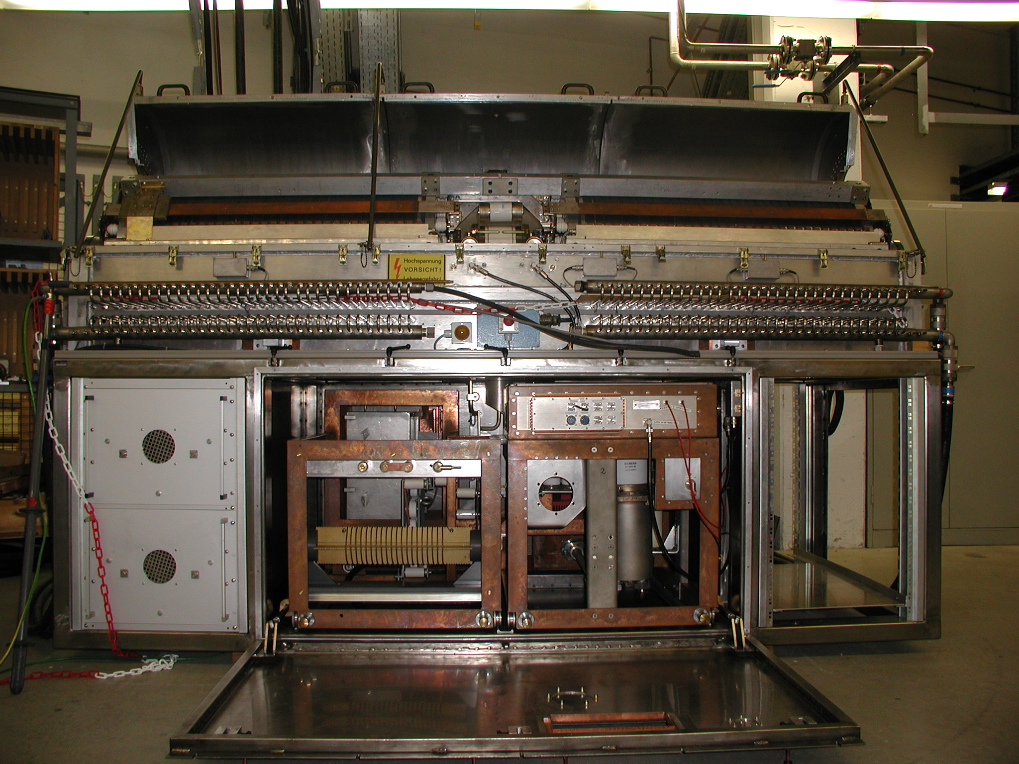
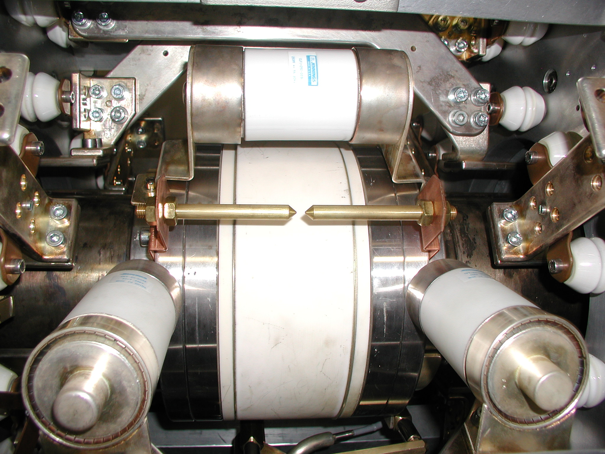
The material Ferroxcube FXC 8C12m is used for the ferrite ring cores. In total, ring cores are used per cavity. Each core has the following dimensions:
For biasing,
figure-of-eight copper windings are present. The total capacitance amounts to
including the gap, the gap capacitors, the cooling disks, and other parasitic capacitances. The maximum voltage that is reached under normal operating conditions is .
| Resonant frequency | |||
|---|---|---|---|
| Relative permeability | |||
| Magnetic bias field at mean radius | |||
| Bias current | |||
| product | |||
| Q-factor | |||
| Cavity time constant |
Table 1 shows the main parameters for three different frequencies. All these values are consistent with the formulas presented in the paper at hand. It is obvious that both and do not vary strongly with frequency justifying the parallel equivalent circuit. This compensation effect was mentioned at the end of Section 0.5.
All the parameters mentioned here refer to the beam side of the cavity. The cavity is driven by an RF amplifier which is coupled to only one of two ferrite core stacks (consisting of 32 ring cores each). The two ring core stacks are coupled by the bias windings. Therefore, a transformation ratio of 1:2 is present from amplifier to beam. This means that the amplifier has to drive a load of about . For a full amplitude of at the power loss in the cavity amounts to .
The SIS18 cavity is supplied by a single-ended tetrode power amplifier using a combination of inductive and capacitive coupling.
It has to be emphasized that the values in Table 1 do not contain the amplifier influence. Depending on the working point of the tetrode, will be reduced significantly, and all related parameters vary accordingly.
0.16 Further practical considerations
For measuring the gap voltage, one needs a gap voltage divider in order to decrease the high-voltage RF to a safer level. This can be done by capacitive voltage dividers. Gap relays are used to short-circuit the gap if the cavity is temporarily unused. This reduces the impedance seen by the beam which may be harmful for beam stability. If cycle-by-cycle switching is needed, semiconductor switches may be used instead of vacuum relays. Another possibility to temporarily reduce the beam impedance is to detune the cavity.
The capacitance/impedance of the gap periphery devices must be considered when the overall capacitance and the other elements in the equivalent circuit are calculated. Also further parasitic elements may be present.
On the one hand, the cavity dimensions should be as small as possible since space in synchrotrons and storage rings is valuable and since undesired resonances may be avoided. On the other hand certain minimum distances have to be kept in order to prevent high-voltage spark-overs. For EMC reasons, RF seals are often used between conducting metal parts of the cavity housing to reduce electromagnetic emission.
In order to fulfil high vacuum requirements, it may be necessary to allow a bakeout of the vacuum chamber. This can be realized by integrating a heating jacket that surrounds the beam pipe. One has to guarantee that the ring cores are not damaged by heating and that safety distances (for RF purposes and high-voltage requirements) are kept.
In case the cavity is used in a radiation environment, the radiation hardness of all materials is an important topic.
0.17 Magnetic materials
A large variety of magnetic materials is available. Nickel-Zinc (NiZn) ferrites may be regarded as the traditional standard material for ferrite-loaded cavities. The following material properties are of interest for the material selection and may differ significantly for different types of material:
-
•
permeability
-
•
magnetic losses
-
•
saturation induction (typically for NiZn ferrites)
-
•
maximum RF inductions (typically mT for NiZn ferrites)
-
•
relative dielectric constant (in the order of for NiZn ferrites but very high for MnZn ferrites, for example) and dielectric losses (usually negligible for typical NiZn applications)
-
•
maximum operating temperature, thermal conductivity, and temperature dependence in general
-
•
magnetostriction
-
•
specific resistance (very high for NiZn ferrites, very low for MnZn ferrites).
In order to determine the RF properties under realistic operating conditions (large magnetic flux, biasing), thorough reproducible measurements in a fixed test setup are inevitable.
Amorphous and nanocrystalline magnetic alloy (MA) materials have been used to build very compact cavities that are based on similar principles to those of classical ferrite cavities (see, e.g., Refs. [21, 15, 22, 6, 23]). These materials allow a higher induction and have a very high permeability. This means that a smaller number of ring cores is needed for the same inductance. MA materials typically have lower Q factors in comparison with ferrite materials. Low Q factors have the advantage that frequency tuning is often not necessary and that it is possible to generate signal forms including higher harmonics instead of pure sine signals. MA cavities are especially of interest for pulsed operation at high field gradients. In case a low Q-factor is not desired, it is also possible to increase it by cutting the MA ring cores.
Acknowledgements
The author would like to thank all the GSI colleagues with whom he discussed several RF cavity issues during the past years, especially Priv.-Doz. Dr. Peter Hülsmann, Dr. Hans Günter König, Dr. Ulrich Laier, and Dr. Gerald Schreiber. He is also grateful to the former staff members of the ring RF group, especially Dr. Klaus Blasche, Dipl.-Phys. Martin Emmerling, and Dr. Klaus Kaspar for transferring their RF cavity know-how to their successors. Last but not least, the author thanks Dr. Rolf Stassen (FZ Jülich) for reviewing the manuscript.
It is impossible to provide a complete list of references. The following list cites only a few references regarding the most important aspects. Many other important publications exist.
References
- [1] J. M. Brennan, in Handbook of Accelerator Physics and Engineering, Eds. A. W. Chao and M. Tigner (World Scientific, Singapore, 1999), pp. 570–2.
- [2] I. D. Mayergoyz, Mathematical Models of Hysteresis and Their Applications, 2nd ed., e-book (Elsevier, San Diego, 2003).
- [3] F. G. Brockman, H. van der Heide, and M. W. Louwerse, Ferroxcube für Protonensynchrotrons, Philips Technische Rundschau, 30 (1969/70) 323–342.
- [4] S. Papureanu, Ch. Hamm, A. Schnase, and H. Meuth, Performance test of a ferrite-loaded cavity under operation conditions, in 15th IEEE Particle Accelerator Conference, Washington, DC, USA, 1993 (IEEE, Piscataway, NJ, 1994), pp. 962–4.
- [5] M. Morvillo, R. Garoby, D. Grier, M. Haase, A. Krusche, P. Maesen, M. Paoluzzi, and C. Rossi, The PS 13.3–20 MHz RF system for LHC, in 20th IEEE Particle Accelerator Conference, Portland, OR, USA, 2003, Ed. J. Chew (JACoW, Geneva, 2003), pp. 1724–6.
- [6] P. Hülsmann, G. Hutter, and W. Vinzenz, The bunch compressor system for SIS18 at GSI, in EPAC, Luzern, 2004, pp. 1165–7.
- [7] W. R. Smythe and T. G. Brophy, RF cavities with transversely biased ferrite tuning, IEEE Trans. Nucl. Sci. NS-32 (1985) 2951–3.
- [8] J. E. Griffin and G. Nicholls, A review of some dynamic loss properties of Ni-Zn accelerator RF system ferrite, IEEE Trans, Nucl. Sci. 26 (1979) 3965–7.
- [9] K. Kaspar, H. G. König, and T. Winnefeld, Studies on maximum RF voltages in ferrite-tuned accelerating cavities, in EPAC, Luzern, 2004, pp. 985–7.
- [10] H. G. König and S. Schäfer, Reduction of Q-loss effects in ferrite-loaded cavities, in EPAC, Genoa, Italy, 2008, pp. 985–7.
- [11] V. S. Arbuzov et al., Accelerating RF station for HIRFL-CSR, Lanzhou, China, in RuPAC XIX, Dubna, 2004, pp. 332–4.
- [12] X. Pei, S. Anderson, D. Jenner, D. McCammon, and T. Sloan, A wide tuning range RF cavity with external ferrite biasing, in 15th IEEE Particle Accelerator Conference, Washington, DC, USA, 1993 (IEEE, Piscataway, NJ, 1994), pp. 1421–3.
- [13] A. Susini, Low frequency ferrite cavities, in EPAC, Rome, 1988, Ed. S. Tazzari (World Scientific, Singapore, 1989), pp. 1416–7.
- [14] I. S. K. Gardner, Ferrite dominated cavities, in CAS - CERN Accelerator School: RF Engineering for Particle Accelerators, Oxford, 1991, S. Turner (Ed.) CERN 92-3, pp. 349–374.
- [15] A. Schnase, Cavities with a swing, in CAS - CERN Accelerator School: Radio Frequency Engineering, Seeheim, 2000, J. Miles (Ed.) CERN 2005-3, pp. 236–272.
- [16] A. Krusche and M. Paoluzzi, The new low frequency accelerating systems for the CERN PS Booster, in EPAC, Stockholm, 1998 (IOP, Bristol, 1998), pp. 1782–3.
- [17] J. Dey, I. Kourbanis, and D. Wildman, A new RF system for bunch coalescing in the Fermilab Main Ring, in 16th IEEE Particle Accelerator Conference, Dallas, TX, USA, 1995 (IEEE, Piscataway, NJ, 1995), pp. 1672–4.
- [18] R. M. Hutcheon, A perpendicular-biased ferrite tuner for the 52 MHz PETRA II cavities, in 12th IEEE Particle Accelerator Conference, Washington, DC, USA, 1987 (IEEE, New York, 1987), pp. 1543–5.
- [19] C. C. Friedrichs, R. D. Carlini, G. Spalek, and W. R. Smythe, Test results of the Los Alamos ferrite-tuned cavity, in 12th IEEE Particle Accelerator Conference, Washington, DC, USA, 1987 (IEEE, New York, 1987), pp. 1896–7.
- [20] R. L. Poirier, Perpendicular biased ferrite-tuned cavities, in 15th IEEE Particle Accelerator Conference, Washington, DC, USA, 1993 (IEEE, Piscataway, NJ, 1994), pp. 753–7.
- [21] C. Fougeron, P. Ausset, D. de Menezes, J. Peyromaure, and G. Charruau, Very wide range and short accelerating cavity for MIMAS, in 15th IEEE Particle Accelerator Conference, Washington, DC, USA, 1993 (IEEE, Piscataway, NJ, 1994), pp. 858–61.
- [22] K. Saito, K. Matsuda, H. Nishiuchi, M. Umezawa, K. Hiramoto, and R. Shinagawa, RF accelerating system for a compact ion synchrotron, in 19th IEEE Particle Accelerator Conference, Chicago, IL, USA, 2001 (IEEE, New York, 2002), pp. 966–8.
- [23] R. Stassen, K. Bongardt, F. J. Etzkorn, H. Stockhorst, S. Papureanu, and A. Schnase, The HESR RF system and tests in COSY, in EPAC, Genoa, 2008 (JACoW, Geneva, 2008), pp. 361–3.
- [24] L. M. Earley, H. A. Thiessen, R. Carlini, and J. Potter, A high-Q ferrite-tuned cavity, IEEE Trans. Nucl. Sci. NS-30 (1983) 3460–2.
- [25] K. Kaspar, Design of Ferrite-Tuned Accelerator Cavities Using Perpendicular-Biased High-Q Ferrites, Technical report, Los Alamos National Laboratory, New Mexico, USA, November 1984, LA-10277-MS.
- [26] G. Schaffer, Improved ferrite biasing scheme for Booster RF cavities, in EPAC, Berlin, 1992 (Éditions Frontières, Gif-sur-Yvette, 1992), pp. 1234–6.