Patterning graphene nanostripes in substrate-supported functionalized graphene: A promising route to integrated, robust, and superior transistors
Abstract
It is promising to apply quantum-mechanically confined graphene systems in field-effect transistors. High stability, superior performance, and large-scale integration are the main challenges facing the practical application of graphene transistors. Our understandings of the adatom-graphene interaction combined with recent progress in the nanofabrication technology indicate that very stable and high-quality graphene nanostripes could be integrated in substrate-supported functionalized (hydrogenated or fluorinated) graphene using electron-beam lithography. We also propose that parallelizing a couple of graphene nanostripes in a transistor should be preferred for practical application, which is also very useful for transistors based on graphene nanoribbon.
pacs:
61.48.Gh, 68.65.-k, 85.30.TvSince the first fabrication and measurement of graphene in 2004novoselov306 , it has become promising in the fields of materials, chemistry, physics, and biology, due to its superior mechanical, electronic and optical properties, low mass density, controllable synthesis, biological compatibility, and so ongeim6 ; wei22 ; rozhkov503 ; singh56 ; molitor23 ; stampfer63 ; sheng_2011 ; bao19 ; liu474 ; bao5 . Graphene transistor is an important application of graphene in these fields, which recently has drawn tremendous interest from both the scientific and industrial communities. The bulk graphene is a semi-metal, and a band gap should be created to achieve high on/off (signal/noise) ratio in graphene transistorsschwierz5 .
.1 High stability, atomically sharp edges, substrate decoupling, and large-scale integration are required for the practical application of graphene nanostructures in field-effect transistors
Quantum-mechanically confining the carriers in graphene nanoribbon (GNR) is an effective and controllable way for the band-gap engineeringchen40 ; han98 ; wang100 ; li319 ; jiao321 ; tao7 . GNRs currently have been fabricated through masked plasma etchingchen40 ; han98 , chemical derivationwang100 ; li319 , unzipping carbon nanotubesjiao321 ; tao7 , nanoparticle etchingcampos9 , surface-assisted self-assemblycai466 , templated self-organizationsprinkle5 , and nanoimprint lithographyliang10 . The band gap of GNR increases inversely with the ribbon width, and a sub-10-nm width is required for a satisfactory on/off ratio in a GNR-based field-effect transistor (GNR-FET) under conventional conditionshan98 ; li319 ; liang10 ; tao7 . Presently, only the masked-plasma etching method has successfully integrated sub-10-nm GNRs on semiconductor substrateyang22 . However, the electronic performance of narrow GNRs is still significantly affected by the edge disorder (caused by the high-energy plasma etching), chemical bonding with unexpected adsorbates, and many detrimental effects from the substrate (additional carrier scattering, intrinsic charge doping, parasitic capacity, and unpredictable disorder-induced gap)wang100 ; koskinen80 ; wang324 ; gallagher81 ; wang4 ; xu11 . Probably due to some edge disorderbai5 , the theoretically predicted spin-polarized transport in zigzag-GNRkim3 has not been experimentally observed. Thus, further improvement in the fabrication of GNR is still required to overcome these obstacles for its practical usage. In addition, large-scale integration is also required for the application of GNR in semiconductor industry.
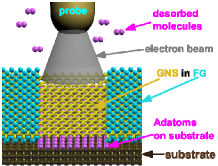
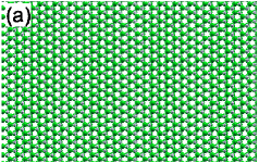
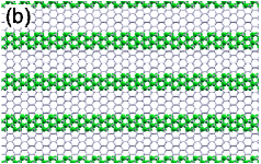
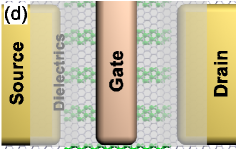
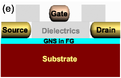
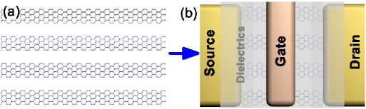
As a counterpart of GNR, the quasi-one-dimensional graphene nanostripe (GNS) sculptured in functionalized (hydrogenated or fluorinated) graphene (FG) has the similar electronic structure as that of GNR, and is regarded as another promising candidate for FETsingh9 ; singh4 ; munoz19 ; ribas4 ; huang_GNS . To obtain superior electronic performance, the edges of GNS, namely the graphene/FG interfaces, should be sharp enough down to the atomic scale, and the fabricated GNS should be robust (without structural changing for a very long time) under conventional conditions. Furthermore, to be an alternative or even a substitute of present silicon-based FETs, large-scale integration of GNS-FET should be readily realized. Scanning-probe lithography is a powerful and miniature electron-beam lithography, which can fabricate nanostructures on surfaces with dimensions even down to several nanometerstseng23 . This method could be used to sculpture sub-10-nm GNSs in FG. The sculpturing process is designed as shown in Fig. 1, in which a GNS is sculptured out in a substrate-supported FG sheet by using a biased scanning probe. The C–X bonds (X is H or F) at the graphene/FG interfaces are broken by the electron-beam excitation. The molecules desorbed upward will escape into vacuum with high escaping velocity, while those downward tend to dissociate again and be adsorbed onto the semiconductor substratehuang_GNS . Those adatoms on the substrate prevent the GNS from covalently bonding with the substrateriedl103 ; robinson11 ; wong_acsnano , which can guarantee the superior electronic performance of the fabricated GNS. Through systematically simulating the kinetics of the adatoms at various graphene/FG interfaceshuang_GNS , we have shown that it is probable to sculpture GNSs with sharp and highly-stable edges in FG. This is because of the considerable increase of the reactivity of the C atoms to H (or F) adatoms with changing the adsorption site from -hybridized GNS to -FGhuang_GNS ; ao97 ; lin78 . Furthermore, scanning-probe lithography should be capable of integrating GNSs in FGtseng23 , which is schematically shown in Fig. 2(a) and (b). Neighboring GNSs can be easily decoupled by just couples of adatom lineslee97 , which indicates that the GNSs could be sculptured very close to but without influencing each other. Thus, high-density integration of GNSs can be realized in FG. In addition, the edges of the experimentally fabricated GNSs in hydrogenatedsessi9 and fluorinated graphenewithers are still not atomically sharp, which is probably due to the fact that the adatom coverage is not high enough in these two experimentshuang_GNS . Thus, to obtain sharp-edge GNSs, it is critical to have FG sheets with high enough adatom coverage.
.2 Parallelizing a couple of GNSs in a FET can make the integrated GNS-FETs perform uniformly and be immune to small structural and environmental perturbations, which also could be generalized to GNR-FET
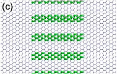
After sculpturing a GNS in a substrate-supported FG sheet, a GNS-FET can be achieved by depositing the source and drain electrodes, dielectrics, and gate electrode, subsequently. However, one important aspect needs a special concern, which is that the electronic correlation in this atomically thick quasi-one dimensional GNS should be quite strong, especially for very narrow GNS. Thus, any small variation in the structure and/or environment will possibly result in an obvious discrepancy in the transport property between different GNSs. This issue may become harmful in large-scale integrated circuits if the unit device (GNS-FET) only consists of one GNS, because it is impossible that the structure and environment of different GNSs in the circuit be strictly all the same. This will introduce additional noise and limit the circuit performance. However, when parallelizing a couple of GNSs in a FET, the variation in the structure, environment, and then the transport property can be averaged out, and the noise will be lowered. The preparation steps for a GNS-FET consisting of a couple of GNSs are schematically shown in Fig. 2(a–e). This parallelization of several transport channels in a FET can be generalized to GNR-FET, too, which is schematically shown in Fig. 3. We could foresee that this parallelization approach can make the integrated FETs perform more uniformly and be immune to small structural and environmental perturbations, and should be preferred for high-quality graphene-based circuits.
In summary, GNS sculptured in FG is a promising nanostructure for graphene transistor. Scanning-probe lithography can be used to obtain integrated, robust, and superior GNSs in substrate-supported FG. It is possible for GNS to overcome some obstacles currently facing the practical application of GNR. Parallelizing a couple of GNSs in a GNS-FET could make all the FETs in an integrated circuit perform uniformly and be immune to the structural and environmental perturbations, which also can be generalized to GNR-FET.
Acknowledgement
This work is supported by the National Science Foundation of China under Grant No. 11174284, National Basic Research Program of China (973 Program) under Grant No. 2012CB933702, Knowledge Innovation Program of Chinese Academy of Sciences, and Director Grants of CASHIPS.
References
- (1) T. P. Chen A. A. Tseng, A. Notargiacomo. J. Vac. Technol. B, 23:877, 2005.
- (2) K. S. Novoselov A. K. Geim. Nat. Mater., 6:183, 2007.
- (3) B. I. Yakobson A. K. Singh. Nano Lett., 9:1540, 2009.
- (4) B. I. Yakobson A. K. Singh, E. S. Penev. ACS Nano, 4:3510, 2010.
- (5) Y. P. Bliokh V. Freilikher F. Nori A. V. Rozhkov, G. Giavaras. Phys. Rep., 503:77, 2011.
- (6) T. Iwasaki A. A. Zakharov U. Starke C. Riedl, C. Coletti. Phys. Rev. Lett., 103:246804, 2009.
- (7) J. Güttinger F. Molitor C. Volk B. Terrés J. Dauber S. Engels S. Schnez A. Jacobsen S. Dröscher T. Ihn K. Ensslin C. Stampfer, S. Fringes. Front. Phys., 6:271, 2011.
- (8) O. V. Yazyev Y. C. Chen J. Feng X. Zhang R. B. Capaz J. M. Tour A. Zettl S. G. Louie S. G. H. Dai M. F. Crommie C. Tao, L. Jiao. Nat. Phys., 7:616, 2011.
- (9) Y. Q. Liu D. C. Wei. Adv. Mater., 22:3225, 2010.
- (10) M. A. Ribas E. S. Penev B. I. Yakobson E. Muñoz, A. K. Singh. Diamond & Related Materials, 19:368, 2010.
- (11) C. Stampfer S. Dröscher A. Jacobsen T. Ihn K. Ensslin F. Molitor, J. Güttinger. J. Phys.: Condens. Matter, 23:243201, 2011.
- (12) M. Dubois S. Russo M. Craciun F. Withers, T. H. Bointon. Nano Lett., 11:3912, 2011.
- (13) Jr. J. Tang J. Bai E. B. Song Y. Huang X. Duan Y. Zhang K. L. Wang G. Xu, C. M. Torres. Nano Lett., 11:1082, 2011.
- (14) C. Cong J. Shang T. Yu H. Wang, Y. Wu. ACS Nano, 4:7221, 2010.
- (15) M. Labella K. A. Trumbull R. Cavelero D. W. Snyder J. A. Robinson, M. Hollander. Nano Lett., 11:3875, 2011.
- (16) F. Xiu L. Liao M. Wang A. Shailos K. L. Wang Y. Huang X. Duan J. Bai, R. Cheng. Nat. Nanotechnol., 5:655, 2010.
- (17) R. Jaafar M. Bieri T. Braun S. Blankenburg M. Muoth A. P. Seitsonen M. Saleh X. Feng K. Müllen R. Fasel R. J. Cai, P. Ruffieux. Nature, 466:470, 2010.
- (18) J. C. Grossman J. H. Lee. Appl. Phys. Lett., 97:133102, 2010.
- (19) S. V. Morozov D. Jiang Y. Zhang S. V. Dubonos I. V. Grigorieva A. A. Firsov K. S. Novoselov, A. K. Geim. Science, 306:666, 2004.
- (20) J. D. Sanchez-Yamagishi J. Kong P. Jarillo-Herro L. C. Campos, V. R. Manfrinato. Nano Lett., 9:2600, 2009.
- (21) G. R. Zhang-L. L. Li Z. Zeng L. F. Huang, X. H. Zheng. J. Phys. Chem. C, 115:21088, 2011.
- (22) G. Diankov H. Wang H. Dai L. Jiao, X. Wang. Nat. Nanotechnol., 5:321, 2010.
- (23) P. B. Sorokin B. I. Yakobson M. A. Ribas, A. K. Singh. Nano Res., 4:143, 2011.
- (24) Y. Zhang P. Kim M. Han, B. Özyilmaz. Phys. Rev. Lett., 98:206805, 2007.
- (25) E. Ulin-Avila B. Geng T. Zentgraf L. Ju F. Wang X. Zhang M. Liu, X. Yin. Nature, 474:64, 2011.
- (26) Y. Hu-J. Hankinson M. Rubio-Roy B. Zhang X. Wu C. Berger M. Sprinkle, M. Ruan. Nat. Nanotechnol., 5:727, 2010.
- (27) D. Goldhaber-Gordon P. Gallagher, K. Todd. Phys. Rev. B, 81:115409, 2010.
- (28) H. Häkkinen P. Koskinen, S. Malola. Phys. Rev. B, 80:073401, 2009.
- (29) M. Bode N. P. Guisinger P. Sessi, J. R. Guest. Nano Lett., 9:4343, 2009.
- (30) B. Wang Z. Ni C. Haley-Y. X. Lim Y. Wang D. Y. Tang K. P. Loh Q. Bao, H. Zhang. Nature, 5:411, 2011.
- (31) Y. Wang Z. Ni Y. Yan-Z. X. Shen K. P. Loh D. Y. Tang Q. Bao, H. Zhang. Adv. Funct. Mater., 19:3077, 2009.
- (32) Y. Wang Z. Shi D. Shi-H. Gao E. Wang G. Zhang R. Yang, L. Zhang. Adv. Mater., 22:4014, 2010.
- (33) Y. Wang L. Cao D. Qi I. Santoso W. Chen A. T. S. Wee S. L. Wong, H. Huang. ACS Nano, 5:7662, 2011.
- (34) F. Schwierz. Nat. Nanotechnol., 5:487, 2010.
- (35) L. Zhai S. Das S. I. Khondaker S. Seal V. Singh, D. Joung. Prog. Mater. Sci., 56:1178, 2011.
- (36) A. D. Güclü M. Zielinski P. Potasz E. S. Kadantsev O. Voznyy P. Hawrylak W. D. Sheng, M. Korkusinski. Front. Phys., 2011.
- (37) A. K. S. Kim W. Y. Kim. Nat. Nanotechnol., 3:408, 2008.
- (38) L. Zhang S. Lee H. Dai X. Li, X. Wang. Science, 319:1229, 2008.
- (39) S. Wu A. Ismach D. L. Olynick S. Cabrini J. Bokor X. Liang, Y. S. Jung. Nano Lett., 10:2454, 2010.
- (40) L. Zhang Y. Yoon P. K. Weber H. Wang J. Guo H. Dai X. Wang, X. Li. Science, 324:768, 2009.
- (41) X. Li H. Wang J. Guo H. Dai X. Wang, Y. Ouyang. Phys. Rev. Lett., 100:206803, 2008.
- (42) B. I. Yakobson Y. Lin, F. Ding. Phys. Rev. B, 78:041402, 2008.
- (43) M. J. Rooks P. Avouris Z. Chen, Y. M. Lin. Physica E, 40:228, 2007.
- (44) F. M. Peeters S. Li Z. M. Ao, A. D. Nernández-Nieves. Appl. Phys. Lett., 97:233109, 2010.