Near-threshold properties of the electronic density of layered quantum-dots
Abstract
We present a way to manipulate an electron trapped in a layered quantum dot based on near-threshold properties of one-body potentials. Firstly, we show that potentials with a simple global parameter allows the manipulation of the wave function changing its spatial localization. This phenomenon seems to be fairly general and could be implemented using current quantum-dot quantum wells technologies and materials if a proper layered quantum dot is designed. So, we propose a model layered quantum dot that consists of a spherical core surrounded by successive layers of different materials. The number of layers and the constituent material are chosen to highlight the near-threshold properties. The manipulation of the spatial localization of the electron in a layered quantum dot results consistent with actual experimental parameters.
pacs:
73.22.-f,73.22.DjI Introduction
The tailoring of particular quantum states has become an usual task in quantum information processing Brunner2011 . Semiconductor quantum dots (QDs) are ideally suited to storage quantum information through its eigenstates, since electrons in QDs can store quantum phase coherence for very long periods of time Takahashi2011 . In addition the amount of entanglement that a multi-electron QD can keep in storage could be useful to implement quantum information tasks, but there exist very few examples of ab initio calculations that attempt to quantify it in the literature FOS ; pots ; pos ; bili ; dami1 ; dami2 . The dots can be designed in a host of ways to meet the specific requirements of the quantum information task in sight, by choosing its shape, size or materials Reimann2002 .
On the other hand, the advances in semiconductor technology allow the preparation of more complex structures than the simple quantum well. Between the more complex structures, the quantum-dot quantum wells structures Schoos1994 and multiple quantum rings Mano2005 have been extensively studied. The quantum-dot quantum wells (QDQW’s) structures are multi-layered quantum dots, composed of two semiconductor materials, the one with the smaller bulk band gap is sandwiched between a core and an outer shell of the material with larger bulk band gap. Because of its properties, the QDQW’s have been demonstrated to form an efficient gain medium for nanocrystal-based lasers Xu2005 , and its electronic structure has been obtained from first-principles calculations Schrier2006 . It is remarkable that the effective mass approximation (EMA) seems to predict fairly well the behavior of the electronic density Schrier2006 ; Berezovsky2005 ; Meier2005 when compared with first-principles calculations.
The quantum ring structures are an ideal playground to study many subtle quantum phenomena as the Aharonov-Bohm effect Bayer2003 which leads to the presence of persistent currents Mailly1993 . This persistent currents have been measured even for one electron states Kleemans2007 . The quantum rings are formed by only one semiconductor material, and the fabrication of multiple concentric quantum rings (up to five) can be achieved with high quality and reliability Somaschini2009 .
Despite all the advantages that quantum dots present as implementations of physical qubits, the confined electrons interact with thousands of spin nuclei through the hyperfine interaction. This leads, inevitably, to decoherence. To solve the decoherence problem it has been proposed that the physical qubit should be implemented by two electrons confined in a double quantum dot Petta2005 . The coupling of the two quantum dots depends on the spatial extent of the one-electron wave functions, in particular it determines the strength of the exchange interaction between the two electrons. The exchange coupling in double quantum dots has been studied extensively, in particular how it can be tuned using electric fields Kwa2009 , magnetic fields Szafran2004 , or the effect of the confinement of the double quantum dot in a quantum wire Zhang2008 . So, the ability to manipulate the spatial extent of the one electron wave function in an isolated QD, can be decisive when dealing with the states of a double quantum dot.
In addition, the recent advances in materials manipulation at the nanoscale allow an accurate shape and size control of the QD that offers the possibility of tailoring the energy spectrum to produce desirable optical transitions. These tasks are useful for the development of optical devices with tunable emission or transmission properties. Optical properties of artificial molecules and atoms are subject of great interest because of their technological implementations. In spherical QD, the optical properties such as the dipole transition, the oscillator strength and the photoionization cross section have been studied theoretically by different authorso1 ; o2 ; o3 ; o4 ; o5 ; o6 .
In this work we present a way to manipulate the wave function of an electron trapped in a quantum dot whose energy is near the continuous threshold. The phenomena associated seem to be fairly general and could be implemented using current quantum-dot quantum wells technologies and materials. In particular we show that the phenomenon is present in a layered quantum dot model whose parameters are consistent with actual experimental values.
The paper is organized as follows. In Sec. II we introduce a simple model whose near-threshold behavior shows how the localization of the ground state electronic density could be handled easily. In Sec. III we apply the findings of Section II to design a QDQW-like model that is both consistent with actual experimental values and able to exploit the near-threshold phenomenon. Here we perform calculations for the ground state and the first excited state, and we analyze the optical properties of the model. Finally, Sec. IV contains the conclusions with a discussion of the most relevant points of our findings.
II One Electron oscillating potential
In this section we report results for the ground state electronic density of one electron in an oscillating short range potential. The near threshold properties will be exploited in the next Section to design quantum dot structures. We choose an smooth and analytical potential to emphasize that the behavior of the electronic density is fairly general. The one particle Hamiltonian is given by
| (1) |
where
| (2) |
where is the strength of the potential and and are positive constants. Clearly, the potential well range is given by and the number of spherical layers and their width are related to . The successive spherical layers are similar to a succession of potential wells and barriers.
It is known that for fixed values of and , there is a critical value such that the Hamiltonian Eq. (1) supports at least one bound state only if kais03 . In the following, we will study the near-threshold properties of the ground state electronic density varying as a global parameter, for .
The ground state energy and wave function of Hamiltonian Eq. (1) were obtained numerically, using the fourth-order Runge-Kutta method for the potential in Eq. 2. The electronic density, , is given by
| (3) |
where is the one-electron wave function. We are interested in the probability of finding the electron in the n-th well. Figure 1 shows the electronic density for different values of . By changing the value of it is possible to select in which potential well the maximum value of the electronic density is located. The particular value of that locates the maximum of the electronic density in, say, the third well depends on the actual values of and .

In Figure 2a we can observe the position where the electronic density achieves its maximum value (). We can check that the value is rather stable as a function of . Moreover, Figure 2a shows that changing allows selecting in which well the electronic density will have its maximum value. It is worth to mention that this effect is a near-threshold phenomenon different from those reported previously in the literature for electrons localized in complex nanostructures Schoos1994 ; Szafran2004 , since in our example the maximum is not necessarily located in the deepest well.
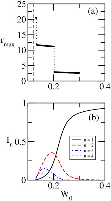
The maximum in the electronic density as a function of the strength potential shows an interesting phenomenon. We can observe how this maximum jumps from a well to the next well when the strength potential is continuously varied. It is important to note that we have a situation where the maximum is not located in the deepest well. In order to clarify this phenomenon we define the “well occupation probability”,
| (4) |
that allows us to evaluate how much of the electronic density is in the n-th well. In figure 2b we show the numerical calculations of for different values of . The intersection of the black solid line () and the red dashed line (), of Figure 2b, give us the value of where a qualitatively change in the electronic density occurs. For this value of we have the first jump. The second jump occurs for the value of where the red dashed line and the blue dashed dotted line intersect.
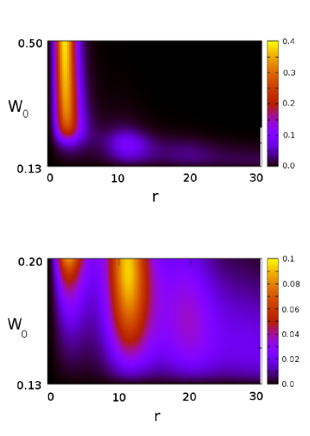
Finally in Figure 3 we plot the Contour map of the electronic density as a function of the coordinate and the strength potential for the potential defined in Eq. (2). Here we can appreciate clearly the effect reported in this work. For larger values of () the electronic density presents just one peak located in the first well. When we decrease the value of we start to see a second (lower) peak located in the second well, but for values of the second peak is higher than the first peak and the maximum is not located in the deepest well. If we continue decreasing the peak in the first well vanishes and we start to appreciate a new peak in the third well.
III One electron QDQW-like model
The ability to produce easily distinguishable quantum states in nanodevices is of fundamental importance because of its potential technological applications, in this sense we show that the spatial extent of the ground state electronic density can be noticeably changed, without changing the spatial extent of the nanostructure.The ground states could be distinguished by current imaging techniques Patane2010 .
On the following we show how our findings could be relevant in actual physical implementations. The synthesis of layered quantum dots is a well known technique, see Reference Schoos1994 and references therein. Moreover, the EMA approximation appropriately describes the electronic structure of nanostructures formed by layers of CdS and HgS. Since the modulation of a global parameter like our is not easily achievable, and that the potential well in CdS/HgS compounds is given by the conduction band offset between the two materials, the only parameters that can be varied with some ease by experimentalist are the width and the materials of the layers. Another difference when dealing with hetero nanostructures with the simple model Hamiltonian in Eq. (1) results from the different effective mass characteristic of each material.
Here we consider structures with two wells made of a HgS layer, separated by one CdS step and with a central CdS core. The step-like potential can be written
| (5) |
where the potential well depth is , which corresponds to the band offset between CdS and HgS, while the effective masses are and respectively Bryant1995 . The width of the inner and outer HgS layers were fixed equal to 2 and 1.5 , respectively, while the width of CdS layer that separates them was fixed to 2 . The width of the central CdS core is going to be varied in order to show the phenomenon presented in previous section. An important difference with is that the width of the layers can be varied easily in the laboratory.
III.1 Ground state electronic density
Here we evaluate the ground state electronic density for the layered QD given by Equation (5), as we did it in the previous section.
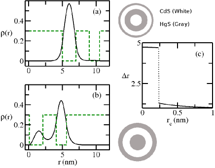
As Figure 4 shows, by changing the width of the CdS core the electronic density maximum can be located in the potential well of election. Besides, the position of the maximum, as a function of the core width, shows the same behavior that the electronic density of the model Hamiltonian, compare the Figure 4c with Figure 2a.
The stability of the electronic density’s maximum can be used when dealing with coupled structures. The fabrication of nanodevices is subjected to many errors so, at least in principle, it could be very useful to have nano-structures whose properties are not excessively sensitive to the actual fabrication parameters.
III.2 Optical Properties
Optical properties are related to the transitions between different states of the quantum system. In this section we need to evaluate the ground state and some of the excited states of the one electron system. As we mentioned before, the phenomenon under investigation is a near threshold property of the system, because of that, the calculation of the excited states requires some effort.
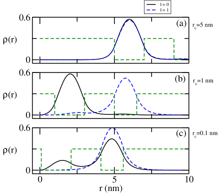
In Figure 5 we show the electronic densities for the ground state and the lower excited state with angular momentum . In Figure 5 (a) we can see that the maximum of both electronic densities are located in the first potential well. As we decrease the width of the central core () we observe that the maximum value of the excited state electronic density jumps to the second potential well while the ground state electronic density remains almost unchanged (Figure 5 (b)). Finally, for small values of the central CdS core we obtain the picture presented before. In Figure 5 (c) we can see that the maximum of both electronic densities ( and ) are located in the second potential well. It is reasonable to assume that this issue must be reflected in the transition rates between these states, and therefore in the optical properties of the one electron QDQW.
It is worth to mention that the overlap between the ground state and the excited state varies from almost one (see Figure 5a) to a very small value (see Figure 5b), and back (see Figure 5c), without changing very much the size of the device. This feature can not be achieved with single well QD without changing its size over one or two magnitude orders since for very large QD the eigenfunctions become very delocalized, resulting in a large overlap between them.
In order to analyze the optical properties of the one electron layered quantum-dots we are going to investigate the electronic dipole-allowed transitions. With this purpose we calculate the Oscillator Strength that is a dimensionless quantity that can be evaluated using the expressionbassani
| (6) |
where is the dipole transition matrix element between the lower () state and the upper state (), and is a normalization constant. Using the Thomas-Reiche-Kuhn sum rule
| (7) |
the normalization constant can be calculated as
| (8) |
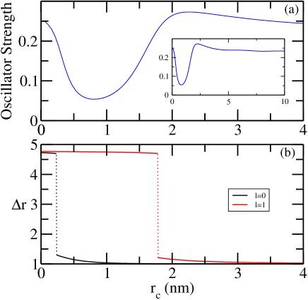
In Figure 6a we can observe the oscillator strength for the transitions between the ground state and the lower excited state with as a function of the core width. In the lower panel, Figure 6b we show, as in Figure 4(c), the behavior of the position where the electronic densities (ground and excited states) achieves its maximum value (), measured with respect to the inner radius of the first potential well as a function of the core width . For large enough values of the CdS core the electronic density maximums lie in the first potential well. As the radius of the CdS core decreases the maximums of the electronic densities jumps to the second potential well ( for the excited state density and for the ground state density), as shown by the abrupt change in . As we can see in the inset of Figure 6a the oscillator strength rapidly decrease for large values of the width of the central CdS core and then reaches to a limit value. The behavior for small values of is rather more complicated, and as was pointed out before, the phenomenon becomes evident. It is clear from Figure 6a and Figure 6b that when the maximum values of the electronic densities are located in different potential wells, the oscillator strength presents a dramatic decrease.
IV Conclusions
We have shown a complete analysis of the ground state of one electron in a spherical potential described in Eq. (2) and (5). We find a effect that, to the best of our knowledge, has not been reported in the literature. For the potential defined in (5) we analyzed the ground and the lower excited state with . The effect mentioned before is also present in the excited state. We finished the present work with the study of the optical properties of the one electron layered quantum-dots. Here we find that the effect is detected by the oscillator strength, that is a very important physical quantity in the study of the optical properties, and is related to the electronic dipole-allowed transitions. Moreover, we can conclude that we can have a great control of the optical properties of these nanostructures in a simple manner using the well known techniques of synthesis of layered quantum dots. A small change in the width of the central core can produce dramatic changes in the optical properties of QDQW.
This phenomenon can be experimentally observed with the actual semiconductor technology. One possible setback for the observation of the phenomenon discussed in this work comes from the low binding energies associated to near-threshold phenomena. Given the fairly simple dependence of the reported phenomenon on the potential characteristics, we believe that its observation is possible and feasible. For the model analyzed in this paper, the availability of materials with larger band offsets could render the phenomenon more pronounced and with larger eigenenergies.
The behavior of the electronic density in one and two dimensional systems with a potential equivalent to Eq. (2) is qualitatively the same. Anyway, since the near-threshold behavior in two dimension is not exactly the same that the observed in three dimensions, it is possible that the jumping of the electronic density between 2-D potential wells could be observed more easily than in the three dimensional case. On the other hand, since in near-threshold two-dimensional systems the wave function rapidly spreads over very large regions, a delicate trade-off between the localization and delocalization could take place.
Other possible extension of our problem to be studied, is its appearance in electrostatic quantum dots Bednarek2003 .
Acknowledgements.
We would like to acknowledge SECYT-UNC, CONICET and MinCyT Córdoba for partial financial support of this project.References
- (1) R. Brunner, Y.-S. Shin, T. Obata, M. Pioro-Ladrière, T. Kubo, K. Yoshida, T. Taniyama, Y. Tokura, and S. Tarucha, Phys. Rev. Lett. 107, 146801 (2011).
- (2) R. Takahashi, K. Kono, S. Tarucha, and K. Ono, Phys. Rev. Lett. 107, 026602 (2011).
- (3) A. Ferrón, O. Osenda and P. Serra, Phys. Rev. A 79, 032509 (2009).
- (4) F. M. Pont, O. Osenda, J. H. Toloza and P. Serra Phys. Rev. A 81, 042518 (2010).
- (5) F. M. Pont, O. Osenda, and P. Serra, Phys. Scr. 82, 038104 (2010).
- (6) M. Bylicki, W. Jaskólski, A. Stachów, and J. Diaz, Phys. Rev. B 72, 075434 (2005).
- (7) J. P. Coe, and I D’Amico J. Phys.: Conf. Ser. 254, 012010 (2010).
- (8) S. Abdullah, J. P. Coe, and I D’Amico Phys. Rev. B 80, 235302 (2009)
- (9) Stephanie M. Reimann and Matti Manninen, Rev. Mod. Phys. 74, 1283 (2002)
- (10) D. Schooss, A. Mews, A. Eychmüller, and H. Weller, Phys. Rev. B 49, 17072 (1994).
- (11) Takaaki Mano, Takashi Kuroda, Stefano Sanguinetti, Tetsuyuki Ochiai, Takahiro Tateno, Jongsu Kim, Takeshi Noda, Mitsuo Kawabe, Kazuaki Sakoda, Giyuu Kido, and Nobuyuki Koguchi, NANO LETTERS 5, 425 (2005).
- (12) J. Xu and M. Xiao, Appl. Phys. Lett. 87, 173117 (2005).
- (13) Joshua Schrier and Lin-Wang Wang, Phys. Rev. B 73, 245332 (2006)
- (14) J. Berezovsky, M. Ouyang, F. Meier, D. D. Awschalom, D. Battaglia, and X. Peng, Phys. Rev. B 71, 081309(R) (2005).
- (15) F. Meier and D. D. Awschalom, Phys. Rev. B 71, 205315 (2005)
- (16) M. Bayer, M. Korkusinski, P. Hawrylak, T. Gutbrod, M. Michel, and A. Forchel, Phys. Rev. Lett. 90, 186801 (2003)
- (17) D. Mailly, C. Chapelier, and A. Benoit, Phys. Rev. Lett. 70, 2020 (1993)
- (18) N. A. J. M. Kleemans, I. M. A. Bominaar-Silkens, V. M. Fomin, V. N. Gladilin, D. Granados, A. G. Taboada, J. M. García, P. Offermans, U. Zeitler, P. C. M. Christianen, J. C. Maan, J. T. Devreese, and P. M. Koenraad, Phys. Rev. Lett. 99, 146808 (2007)
- (19) C. Somaschini, S. Bietti, N. Koguchi, and S. Sanguinetti, Nano Letters 9, 3419 (2009)
- (20) R. Petta, A. C. Johnson, J. M. Taylor, E. A. Laird, A. Yacoby, M. D. Lukin, C. M. Marcus, M. P. Hanson, A. C. Gossard, Science 309, 2180 (2005).
- (21) A. Kwasniowski and J. Adamowski, J. Phys: Condens. Matter 21, 235601 (2009)
- (22) L.-X. Zhang, D. V. Melnikov, S. Agarwal, and J.-P. Leburton, Phys. Rev. B 78, 035418 (2008).
- (23) B. Szafran, F. M. Peeters, and S. Bednarek, Phys. Rev. B 70, 125310 (2004)
- (24) J. L. Gondar and F. Comas, Physica B 322, 413 (2003).
- (25) S. Yilmaz and H. Safak, Physica E 36, 40 (2007).
- (26) A. Özmen, Y. Yakar, B. Cakir and Ü. Atav, Opt. Commun, 282, 3999 (2009).
- (27) J. S. deSousa, J. P. Leburton, V. N. Freire, and E. F. daSilva, Phys. Rev. B 72, 155438 (2005).
- (28) I. Karabulut and S. Baskoutas, J. Appl. Phys 103, 073512 (2008).
- (29) M. Sahin, Phys. Rev. B 77, 045317 (2008).
- (30) A. Harju, S. Siljamäki, and R. M. Nieminen, Phys. Rev. Lett. 88, 226804 (2002).
- (31) A. Patanè, N. Mori, O. Makarovsky, L. Eaves, M. L. Zambrano, J. C. Arce, L. Dickinson, and D. K. Maude, Phys. Rev. Lett. 105, 236804 (2010).
- (32) S. Kais y P. Serra, Adv. Chem. Phys. 125, 1 (2003).
- (33) G.W. Bryant, Phys. Rev. B 52, R16997 (1995)
- (34) R. Buczko and F. Bassani, Phys. Rev. B 54, 2667 (1996)
- (35) S. Bednarek, B. Szafran, K. Lis, and J. Adamowski, Phys. Rev. B 68, 155333 (2003)