Direct Measurement of the Fermi Energy in Graphene Using a Double Layer Structure
Abstract
We describe a technique which allows a direct measurement of the relative Fermi energy in an electron system using a double layer structure, where graphene is one of the two layers. We illustrate this method by probing the Fermi energy as a function of density in a graphene monolayer, at zero and in high magnetic fields. This technique allows us to determine the Fermi velocity, Landau level spacing, and Landau level broadening in graphene. We find that the Landau level broadening is larger by comparison to the broadening of upper and lower Landau levels.
pacs:
73.43.-f, 71.35.-y, 73.22.GkThe Fermi energy is a fundamental property of an electron system, and thermodynamic measurements which probe the Fermi energy or density of states are key to understanding the host material band structure and electron interaction effects. Although a number of thermodynamic properties, such as specific heat gornik1985 ; wang1992 , magnetization jp1985 , magnetocapacitance smith , or compressibility jp1994 can directly probe the density of states in an electron system, accessing them experimentally becomes increasingly difficult at the micro- and nano-scale. In the case of graphene geim , magnetization and specific heat measurements are exceedingly difficult, and the accuracy of compressibility jp2010 and capacitance measurements ponomarenko ; young ; droscher are also limited by the reduced sample dimensions. Using a double layer device structure where graphene is one of the layers, we describe a technique which allows a direct measurement of the Fermi energy in an electron system with an accuracy which is independent of the sample size. The underlying principle of the method discussed here is that an interlayer bias applied to bring the graphene layer to the charge neutrality point is equal to the Fermi energy of the opposite electron system. We illustrate this technique by probing the Fermi energy in a graphene layer, both at zero and in high magnetic fields. We show that this method allows an accurate determination of the Fermi velocity in graphene, the Landau level spacing, and Landau level broadening in high magnetic fields.
Our samples are independently contacted graphene double layers, consisting of two graphene single layers separated by a thin dielectric as shown in Fig. 1(a) kim . To fabricate such devices, we first mechanically exfoliate the bottom graphene layer from natural graphite onto a 280 nm thick SiO2 dielectric, thermally grown on a highly doped Si substrate. Standard e-beam lithography, Cr/Au deposition followed by lift-off, and O2 plasma etching are used to define a Hall bar device. A 4 to 7 nm top Al2O3 dielectric layer is deposited on the bottom layer by atomic layer deposition, and using evaporated Al as a nucleation layer. The dielectric film thickness grown on graphene is further verified by transmission electron microscopy in multiple samples. To fabricate the graphene top layer, a separate graphene single layer is mechanically exfoliated on a SiO2/Si substrate. After spin-coating polymetyl metacrylate (PMMA) on the top layer and curing, we etch the underlying substrate with NaOH, and detach the top layer along with the alignment markers captured in the PMMA membrane. The membrane is transferred onto the bottom layer device, and aligned. A Hall bar is subsequently defined on the top layer, completing the double layer graphene device. Three samples were investigated in this study, all with similar results. We focus here on data collected from one sample with a 7.5 nm thick interlayer dielectric, and with an interlayer resistance larger than 1 G. Both layer mobilities are 10,000 cm2/Vs. Using small signal, low frequency lock-in techniques we probe the layer resistivities as a function of back-gate bias (), and the inter-layer () bias applied on the top layer. The bottom layer is maintained grounded during measurements.
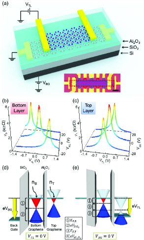
Figure 1(b,c) data show the longitudinal resistivity of the bottom () and top () layer measured as a function of , and at different values gate_bias . The data vs. exhibit the ambipolar behavior characteristic of graphene, and with a charge neutrality point which is -dependent. The shift of the charge neutrality point of the bottom layer as a function of is explained by picturing the bottom layer as a dual-gated graphene single layer, with the Si substrate as back-gate and the top graphene layer serving as top-gate. The dependence of the vs. data on is more subtle, and implies an incomplete screening by the bottom layer of the back-gate induced electric field.
We can quantitatively explain the top and bottom layer density dependence on and using a simple band diagram model. Figure 1(d) shows the band diagram of the graphene bilayer at a finite , and with both layers at ground potential. For simplicity the back-gate Fermi energy and the two graphene layers charge neutrality points are assumed to be at the same energy at V. Once a finite is applied, charge densities are induced in both bottom (), and top () layers. Consequently electric fields are built-in across both bottom SiO2 and inter-layer Al2O3 dielectric. The applied potential is the sum of the potential drop across the SiO2 dielectric and the Fermi energy of the bottom layer:
| (1) |
Here, represents the Fermi energy of the bottom layer corresponding to a charge density , and measured from the charge neutrality point; and are positive when the carriers are electrons, and negative when the carriers are holes. denotes the bottom dielectric capacitance per unit area.
Figure 1(e) shows a similar band diagram of the graphene bilayer, but in the presence of a finite inter-layer bias and at V. Similarly to Fig. 1(d), the applied bias can be written as the sum of the potential drop across the Al2O3 dielectric and the Fermi energies of the two layers:
| (2) |
Here, represents the Fermi energy of the top layer at a charge density , and is the interlayer dielectric capacitance per unit area. In Fig. 1(e) the bias is assumed to be positive, resulting in electrons (holes) induced in the bottom (top) layer. Although we derived Eqs. (1) and (2) assuming V, and V respectively, the two equations hold at all and values. Most importantly, we do not make any assumption with regard to the dependence on and . As we show below, this dependence will be determined experimentally.
Figure 2(a) data show contour graphs of (left panel) and (right panel) as a function of and . The bottom layer resistivity dependence on gate bias is very similar to a dual-gated graphene monolayer kim , showing an almost linear dependence of the charge neutrality point on and , with a slope equal to the ratio. Using nF/cm2 for the bottom SiO2 dielectric, we determine the inter-layer dielectric capacitance to be nF/cm2. The capacitance values are confirmed by Hall measurements.
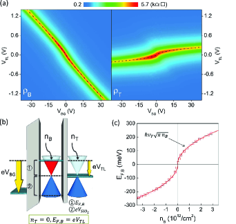
The top layer resistivity shows the characteristic ambipolar behavior as a function of , and with a weaker dependence. Let us examine more closely the top layer charge neutrality point dependence on and . If we consider the top layer at the charge neutrality point, setting in Eq. (2) yields:
| (3) |
This equation contains a simple, yet remarkable result. The inter-layer bias required to bring the top layer at the charge neutrality point is equal to the Fermi energy of the opposite layer, in units of eV [Fig. 2(b)]. Consequently, tracking the top layer charge neutrality point in the - plane [dash-dotted trace in Fig. 2(a) left panel], results in a measurement of the bottom layer Fermi energy as a function of . Furthermore, setting in Eq. (1), and using Eq. (3) allows for to be determined as a function of and along the top layer charge neutrality line of Fig. 2(a):
| (4) |
Equations (3) and (4) provide a direct measurement of the bottom layer Fermi energy as a function of density. To illustrate this, in Fig. 2(c) we show the bottom layer Fermi energy as a function of , determined using Fig. 2(a) data and Eqs. (3) and (4). The values are in excellent agreement with the dependence expected for the linear energy-momentum dispersion of graphene, and with an extracted Fermi velocity of cm/s.
In the following we show that the above method applies equally well to an electron system in high magnetic fields, allowing a direct measurement of Landau level (LL) energies and broadening. In Fig. 3(a) we show the contour plots of (top panel) and (bottom panel) measured as a function of and in an applied perpendicular magnetic field T. Both layers show quantum Hall states (QHS) marked by vanishing resistitvities at filling factors , consistent with a graphene monolayer novoselov2005 ; zhang2005 . The integer represents the Landau level index. The top panel of Fig. 3(a) data shows a step-like dependence of the top layer charge neutrality point on and . Similarly to Fig. 2, substituting with at the top layer charge neutrality line in Fig. 3(a) (top panel) provides a mapping of as a function of . To visualize this, the top layer charge neutrality line in the plane is superposed with the contour plot of Fig. 3(b) (bottom panel), which shows step-like increments of coinciding with the QHSs of the bottom layer.
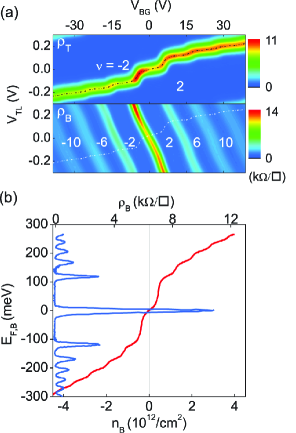
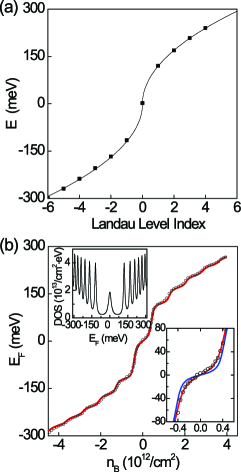
Figure 3(b) shows vs. at T determined by tracking the top layer charge neutrality line in the plane in Fig. 3(a), and using Eqs. (3) and (4) to convert and into and , respectively. In addition, Fig. 3(b) shows vs. , determined by tracking the bottom layer resistivity along the top layer charge neutrality line [dashed-dotted line of Fig. 3(a)]. Figure 3(b) data manifestly shows the staircase-like behavior expected for the Fermi level dependence on density for a two-dimensional electron system in a perpendicular magnetic field. The peaks in the vs. data of Fig. 3(b), corresponding to the Fermi level lying in the LL center and probing extended states, correlate with plateaus in the vs. , associated with the large LL density of states. The peaks in the vs. data of Fig. 3(b) provide a direct measurement of the LL energy. Figure 4(a) summarizes the bottom graphene layer LL energy as a function of index () at T. The experimental data is in excellent agreement with the theoretical dependence , corresponding to a Fermi velocity cms, a value less than 2 different than the Fermi velocity determined at T using Fig. 2 data.
In Figure 4(b) we compare the vs. data determined experimentally at T, with calculations. Assuming a Lorentzian distribution of the disorder-induced LL broadening, the density of states writes:
| (5) |
with being the broadening of the -th LL. The carrier density () dependence on in the limit K is:
| (6) |
Using Eqs. (5) and (6), the best fit to vs. data is obtained for meV, and meV for . The summation in Eq. (5) does not converge if carried out to infinity, and a high-energy cut-off is customarily used. For the calculations of Fig. 4(b) we used in Eq. (5), corresponding to a 1 eV cut-off energy; increasing the cut-off LL index to 1,000, will change the best fit value by less than 0.5 meV. The lower inset of Fig. 4(b) shows a comparison of the vs. experimental data with calculations using the same broadening for the LL as the upper and lower LLs, meV. The larger broadening of the LL by comparison to the other LLs is an interesting finding. A theoretical study zhu2009 , which examined the impact of static disorder on LL broadening in graphene without considering interaction showed that the LL broadening is the same as for the other LLs. On the other hand electron-electron interaction can impact the broadening of the four-fold degenerate LL, and experimental data on exfoliated graphene on SiO2 substrates show a splitting of the LL in high, T magnetic fields zhang2006 , explained as a many-body effect. Lastly, we note that a Gaussian-shaped Landau levels density of states yields worse fits to Fig. 4 data, by comparison to the Lorentzian shape density of states. Scanning tunneling microscopy studies li ; miller , and compressibility measurements in graphene jp2010 also favor the Lorentzian LL lineshape by comparison to the Gaussian one. A recent theoretical study argues that LL local density of states has a Lorentzian lineshape while the total density of states is Gaussian zhu2011 . Presumably, the sample size examined here, defined by a 4 m Hall bar width coupled with the 8 m top layer contact spacing is sufficiently small such that the Lorentzian LL line-shape dominates.
In summary, we present a method to determine the Fermi energy in a two-dimensional electron system, using a double layer device structure with one layer consisting of graphene. We illustrate this technique by probing the Fermi energy in a separate graphene layer as a function of density at zero, and in a high magnetic field, and determine with high accuracy the Fermi velocity, and the Landau level broadening. The technique sensitivity is independent of the sample dimensions, which makes it applicable to a variety of nanoscale materials.
We thank C. P. Morath and M. P. Lilly for technical discussions. This work was supported by NRI, ONR, and Intel. Part of this work was performed at the National High Magnetic Field Laboratory, which is supported by NSF (DMR-0654118), the State of Florida, and the DOE.
References
- (1) E. Gornik, R. Lassnig, G. Strasser, H. L. Stormer, A. C. Gossard, W. Wiegmann, Phys. Rev. Lett. 54, 1820 (1985).
- (2) J. K. Wang, D. C. Tsui, M. Santos, and M. Shayegan, Phys. Rev. B 45, 4384 (1992).
- (3) J. P. Eisenstein, H. L. Stormer, V. Narayanamurti, A. Y. Cho, A. C. Gossard, C. W. Tu, Phys. Rev. Lett. 55, 875 (1985).
- (4) T. P. Smith, B. B. Goldberg, P. J. Stiles, M. Heiblum, Phys. Rev. B 32, 2696 (1985).
- (5) J. P. Eisenstein, L. N. Pfeiffer, and K. W. West, Phys. Rev. B 50, 1760 (1994).
- (6) A. K. Geim, K. S. Novoselov, Nature Materials 6, 183 (2007).
- (7) E. A. Henriksen, and J. P. Eisenstein, Phys. Rev. B 82, 041412(R) (2010).
- (8) L. A. Ponomarenko et al., Phys. Rev. Lett. 105, 136801 (2010).
- (9) A. F. Young et al., arXiv:1004.5556 (2010).
- (10) S. Droscher, P. Roulleau, F. Molitor, P. Studerus, C. Stampfer, K. Ensslin, and T. Ihn, Appl. Phys. Lett. 96, 152104 (2010).
- (11) S. Kim, I. Jo, J. Nah, Z. Yao, S. K. Banerjee, and E. Tutuc, Phys. Rev. B 83, 161401 (2011).
- (12) For simplicity and are referenced with respect the bias values at which both layers are at the Dirac point: V, V.
- (13) K. S. Novoselov et al., Nature 438, 197 (2005).
- (14) Y. Zhang et al., Nature 438, 201 (2005).
- (15) W. Zhu, Q. W. Shi, X. R. Wang, J. Chen, J. L. Yang, and J. G. Hou, Phys. Rev. Lett. 102, 056803 (2009).
- (16) Y. Zhang et al., Phys. Rev. Lett. 96, 136806 (2006).
- (17) G. Li, A. Luican, E. Y. Andrei, Phys. Rev. Lett. 102, 176804 (2009).
- (18) D. L. Miller, K. D. Kubista, G. M. Rutter, M. Ruan, W. A. de Heer, P. N. First, J. A. Stroscio, Science 324, 924 (2009).
- (19) W. Zhu, H. Y. Yuan, Q. W. Shi, J. G. Hou, X. R. Wang, Phys. Rev. B 83, 153408 (2011).