Field induced quantum-Hall ferromagnetism in suspended bilayer graphene
Abstract
We have measured the magneto-resistance of freely suspended high-mobility bilayer graphene. For magnetic fields T we observe the opening of a field induced gap at the charge neutrality point characterized by a diverging resistance. For higher fields the eight-fold degenerated lowest Landau level lifts completely. Both the sequence of this symmetry breaking and the strong transition of the gap-size point to a ferromagnetic nature of the insulating phase developing at the charge neutrality point.
pacs:
73.22.Pr,73.43.-f,71.70.Di,73.43.QtI Introduction
The unique electronic properties of monolayer and bilayer graphene makes them promising candidates for future applications in nanotechnology. Though (bilayer) graphene on a SiO2-substrate can show a mobility up to 2 m2/Vs,Geim and Novoselov (2007) much cleaner and higher mobility samples are necessary in order to investigate its intrinsic properties, and, in particular, electron interaction effects. Mobilities exceeding 10 m2/Vs can be obtained by removing the SiO2 substrate underneath the grapheneBolotin et al. (2008); Du et al. (2008) or by depositing graphene on a boron nitride crystal.Dean et al. (2010) These high-mobility samples display new interaction-induced phenomena such as a fractional quantum Hall effect,Dean et al. (2011); Bolotin et al. (2011); Du et al. (2009) broken-symmetry states,Feldman et al. (2009) a magnetic-field induced insulating phase,Feldman et al. (2009) and quantized conductance at zero magnetic field.Tombros et al. (2011)00footnotetext: check list mobilities on end
In the two-dimensional electron system of bilayer graphene (BLG) the application of a perpendicular magnetic field results into an unconventional integer quantum Hall effect with plateaus at filling factors = , …Novoselov et al. (2006) The lowest Landau level is eight-fold degenerate, owing to spin, valley and layer-index degrees of freedom. In standard BLG samples deposited on SiO2, magnetic fields around 10 T are required to observe fully quantized plateaus and the eight-fold degeneracy of the lowest Landau level is only lifted for the highest quality samples at magnetic fields exceeding 20 T.Zhao et al. (2010) At 0 T the density of states in BLG does not vanish at the charge neutrality point, in contrast to single layer graphene, therefore, even arbitrarily weak interaction between charge from conduction and valence band states will trigger excitonic instabilities which causes a variety of gapped states.Nandkishore and Levitov (2010, 2010); Zhang et al. (2011); Jung et al. ; Martin et al.
In this paper, we present two-terminal magnetotransport experiments in suspended BLG at temperatures ranging from 1.3 K to 4.2 K and magnetic fields up to 30 T. We observe a sudden gap opening at the CNP already for 1 T and the appearance of broken-symmetry states at filling factors for higher fields. Detailed investigation of the energy gap at filling factor = 0 reveals an exchange-interaction driven linear scaling at low magnetic fields, in agreement with earlier reported results.Feldman et al. (2009) At high fields we observe the cross-over to a much smaller gap. This high field transition and the appearance of broken symmetry states at = 1, 2, 3 are consistent with the formation of a quantum Hall ferromagnetic state.Barlas et al. (2008); Nandkishore and Levitov (2010)
II Experimental background
We have prepared a suspended BLG sample using an acid free method.Tombros et al. (2011) Following standard techniques, Novoselov et al. (2004) we first exfoliated flakes from highly oriented pyrolytic graphite (HOPG) and deposited them on a Si/SiO2 substrate covered with a 1.15 m thick LOR-A resist layer. Bilayer flakes were then identified by their optical contrast. Blake et al. (2007) Subsequently, two electron beam lithography steps were performed in order to contact the flakes with Ti-Au contacts and to remove part of the LOR-A below the graphene flakes. The resulting device is freely suspended across a trench formed in the LOR-A with two metallic contacts on each side, see inset of Fig. 1.
Carriers in the BLG sheet can be induced by applying a back-gate voltage on the highly -doped Si wafer. The geometrical gate capacitance is given by a combination of the vacuum gap (1.15 m) and SiO2 substrate (0.5 m).
Using a serial capacitor model we calculate a gate capacitance of 7.2 aF/m-2 which directly relates the carrier concentration to as with leverage factor m-2V-1 and a finite voltage of the the CNP of = 1.2 V. In high magnetic fields, the geometric capacitance increases due to the formation of edge statesVera-Marun et al. (2011) and becomes dependent on . Therefore, the exact values of capacitance were determined experimentally by identifying the filling factors of quantized Hall plateaus in magnetic field, details can be found in the appendix.
After mounting the devices were slowly cooled down to 4.2 K and current annealed Moser et al. (2007) by applying a DC bias current up to 3 mA. This local annealing resulted into the high quality sample with mobility 10 m2/Vs at a charge carrier density . The value of the mobility is calculated based on the dimension of suspended graphene before current annealing: 0.3 m wide and 2.1 m long. However, in the membrane the distribution of the temperature while current annealing is non homogenous,Tombros et al. (2011) which most probably leads to the middle
part of the membrane being annealed and non annealed regions close by the contacts. In this case the estimation of the mobility value based on geometrical dimensions might be not precise. We can also estimate the quality of obtained sample from the value of magnetic field at which the system enters the quantum Hall regime (B 0.5 T). Assuming for QHE to existBolotin et al. (2008), the observation applies a lower bound for the mobility of 2 m2/Vs.
Measurements were performed with standard low-frequency lock-in techniques in two-probe geometry with an excitation current of 2 nA.
III Results
In Fig. 1 we show the data for the two-point resistance of our suspended BLG device at = 0 T and = 1 T as a function of (top x-axis) and (bottom x-axis), respectively. The two-probe resistance is characterized by a magnetoresistance with superimposed Hall-resistance , . Here is the aspect ratio of the device. The traces are corrected by phenomenological contact resistances (1 k on the electron-side and 1.7 k on hole-side) which were determined from a finite resistance background observed at high carrier concentrations; this background resistance increases by about a factor 2 in the range = 0…30 T. These contact resistances most probably originate from in-series connected non-annealed parts of the sample,Abanin and Levitov (2008) contact dopingHuard et al. (2008); Blake et al. (2009) and the finite resistance of the current leads. The sharp maximum at the CNP of the zero-field data already indicates the high electronic quality of the sample. At 1 T the resistance already exhibits fully quantized plateaus at filling factors and a developing quantization at and . The formation of these plateaus is caused by a quantization of and the associated zero minima in when the Fermi energy lies between two Landau levels Novoselov et al. (2006) and confirms the high electronic mobility () of our device required to observe this unconventional quantum Hall effect.
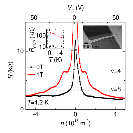
Additionally, as soon as a finite magnetic field is applied, the resistance at the CNP, , starts to diverge. Whereas at zero magnetic field is only very weakly temperature dependent and comparable to the resistance quantum, already at 1 T it is nearly an order of magnitude higher and starts to increase strongly with decreasing temperature, see left inset in Fig. 1. The nature of the gap opening at the CNP is elucidated further in Fig. 2a where we show the resistance as a function of carrier concentration for several magnetic fields. The diverging resistance at the CNP appears at similar magnetic field as the plateaus at filling factors -4 and 4; i. e. the eight-fold degeneracy of the zero-energy Landau level breaks directly into two four-fold degenerated Landau levels, as already predicted theoreticallyMcCann (2006) and proven experimentally.Kim et al. (2011) At low fields 0.1 T we observe a small decrease of the resistance maximum at the CNP (not shown in the figure). This small decrease in resistance can be explained by the presence of local inhomogeneities which give a small splitting between the valley-polarized energies; the cross-over of these energy-states at finite magnetic field results in a resistance minimum. When the magnetic field is above 0.1 T we observe a rapid increase of the resistance-maximum at the CNP, shown in Fig. 2b. We can interpret this rapid increase as a result of the spin-splitting of the two energy levels at zero energy or by disorder, e.g. unevenly charged top and bottom layer. The last scenario would lead to a strong temperature dependence at zero field and ultimately for big disorder to an insulating state at zero field, as discussed in Ref. Veligura et al., 2012. The absence of a temperature influence at 0 T and the CNP centered at very low gate-voltage points to a non-disordered bilayer, therefore we interpret the rapid increase by a result of spin splitting.
The absence of an energy-level at in the inset of Fig. 2b results in a diverging resistance at the CNP. The resistance at the CNP follows a classical Ahrrenius-activation behaviour , in where is a scale for the size of the gap. The resistance increase scales best with , from which we obtain a gap . This gap is about a factor 3 times larger than the Zeeman-splitting , which can be explained by the dominating exchange energy.Kurganova et al. (2011) Equation (1) describes the total spin energy , determined by the sum of the single electron Zeeman energy and the exchange energy . Here is the normalized difference between spin-up and spin-down occupation.
| (1) |
At low fields the two energy levels are still overlapping and the system is not fully spin polarized, . Assuming Gaussian shaped Landau levels we can approximate with leads with help of equation (1) to the gap . The observed spin-enhancement by a factor 3 corresponds to a typical level width = 2 meV and exchange energy = 1.3 meV at = 1 T corresponding to a value of about 2 % of the Coulomb energy = 56 meV, where is the magnetic length.
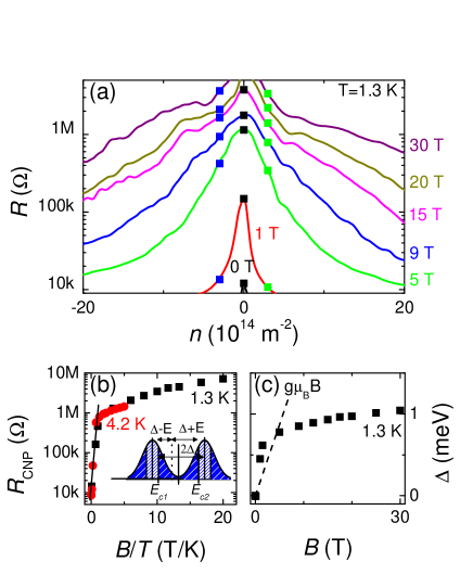
The behavior at high magnetic field is experimentally more complicated to access, because the measured resistance rapidly exceeds several Ms and a quantitative analysis becomes difficult. However away from the CNP the measured resistances stay low enough to guarantee a reliable interpretation up to the highest magnetic fields. This situation is illustrated in the inset of Fig. 2b where we sketch the quantized density of states in the lowest Landau level around the CNP with a gap 2 opening at . When the Fermi energy is located at a finite energy (i.e. still inside the localized parts of the DOS), conduction will occur by thermal excitation to the conductivity edges and of the extended states. The resistance at this energy will then be given by
| (2) |
For relatively small energies the cosh-term can be approximated by a first order Taylor expansion . For small we can interpret equation (2) as . At the CNP, , this approaches a trivial Ahrrenius-behavior, while for non-zero fixed energy is an energy dependent renormalization factor which for is independent of .
We analyze the resistance at concentrations m-2 (dots marked in Fig. 2a and multiply this data with a fixed constant to make an overlap with the low field data). All datapoints 1 M in Fig. 2b are verified by this method and therefore reliable up to the highest field. This proper scaling for both low and high resistances also excludes a strong effect of the local heating due the finite excitation voltage we apply over the sample.
From Fig. 2b we see that the scaling of the resistance at high magnetic fields is remarkably different from the linear field increase at low fields. This observation is again visualized in Fig. 2c where we show that the calculated gap strongly bends and the slope strongly reduces. In this regime the gatesweeps are packed more densly for increasing magnetic field and the energy gets comparable to the thermal activation thus we are no longer able to calculate the gap-size with a simple Arrhenius-behaviour. Experimental limitations of our suspended samples do not allow us to access much higher temperatures, therefore we can only speculate here about further gap-study.
At high enough fields we expect to fulfill the criteria of fully spin-polarized system, . The sudden strong change of the gap-size suggests that our system indeed gets fully spin-polarized, in literature also known as the cross-over to a quantum Hall ferromagnetic state. Further increase of the magnetic field leads hypothetically to a dominating spin-splitting , because . Further specific research in titled magnetic fields is necessary to decouple the influence of the single electron Zeeman energy and exchange energy.
After detailed study at low concentrations we have a closer look at the manifestation of the QHE at higher concentration. In Fig. 3a we show the corrected two-point resistance as a function at 4.2 K for = 1 T, 5 T, 12 T, 17.5 T and 30 T. Apart from the distinct plateaus which are already well pronounced at 1 T, additional plateaus at and start to appear in higher fields. In Fig. 3b we show the derivative of the resistance curves, where we can already already recognize distinct maxima and minima for lower fields.
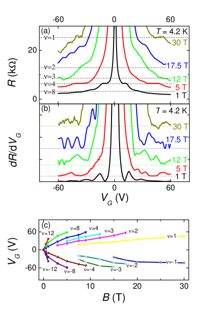
In Fig. 3c we follow the position of the minima with increasing magnetic field. We see that the maximum applied gate-voltage = 60 V limits the observation of filling factors up to 9 T, while remains observable till fields of 15 - 20 T and filling factor is still observable at the highest applied field, 30 T. From Fig. 3c we observe that the position of the minima strongly deviates from the linear relationship between the induced charge carrier concentration and the applied magnetic field , . The equidistance of the minima for fixed magnetic fields excludes a capacitance-change due the bending of the membrane; which can be expected by the particular big difference between the electric field induced bending (10 - 20 nm)Wang et al. (2010) and the vacuum gap over which graphene is suspended (m). In the appendix we discuss in more detail how to extract the exact relation between the applied field and the induced charge concentration from this data.
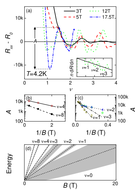
Experiments on suspended graphene-samples are mainly performed in two-probe configuration. Experimental limitations of the annealing-procedure do not allow us to obtain very homogenous samples in four-probe configuration. Therefore more effort has to be done to do a proper analysis on both the magnetoresistance and Hall-resistance. In Fig. 4 the appearance of the different filling factors are further elucidated; in particular at positive gate-voltages, the influence of contact-resistance is here experimentally the smallest. As shown in Fig. 3b the derivative of our data, , shows already at very low field a very clear appearance of filling factors = 1, 2, 3 and 4. A small change in the slope of causes a very distinct minimum in the derivative. Theoretically we can use a model that directly describes the magnetoresistance in terms of the Hall resistance ,Stormer et al. (1992) i.e. . In Fig. 4a we study the appearance of the filling factors by plotting the obtained magnetoresistances . Here we removed from all data the linear background of the 12 T data shown in the inset of Fig. 4a and centered all curves around the x-axis. We used the obtained leverage factor to determine the exact concentration . Already at 3 T we observe the appearance of clear oscillations around and followed by the appearance of at 5 T. The amplitude of the oscillation is defined by the difference between the minimum and the first maximum. A single oscillation can be best analyzed by applying Lifshitz-Kosevic equationLifshitz and Kosevich (1956) , here is the amplitude and a field-dependent function that determines the frequency and phase. The amplitude is finite due to the Landau-level broadening, and is damped by the Dingle-factor in where is the Dingle-temperature, the cyclotron mass in units of electron mass , the magnetic field and T/K. In Fig. 4b the amplitudes for and are plotted as function of , which affects in a linear decrease with slope . If we assume the cyclotron mass in bilayer graphene to be (corresponding to = 0.4 eV, see Ref. Kurganova et al., 2010 and references in there) we obtain the Dingle temperatures in the table below. We repeat the same procedure for filling factors 1, 2 and 3 in Fig. 4c.
| 8 | 4 | 3 | 2 | 1 | |
|---|---|---|---|---|---|
| (K) |
Compared to , fully quantized at T, the Dingle temperatures for the degenerate filling factors are one order of magnitude larger, which means fields 10 T are required to observe full quantization; in particular filling factor becomes quantized at fields of 30 T.
In Fig. 4 we illustrate qualitatively the appearance of the different Landau-levels for increasing magnetic field. The corresponding grey shaded areas describe the Landau level broadening , directly determined by the Dingle temperature ; higher Dingle temperatures correspond broader Landau levels. While the position of the energy moves linearly with increasing field, the Landau level broadening is proportional to the square root of the applied field . With increasing field the overlap between the shaded areas decreases, and the plateau starts to appear. As we can see from Fig. 4d Landau levels around and do indeed not overlap anymore for similar magnetic field, however the shaded areas for overlap till higher fields. Finally the overlapping of filling factors disappears at similar magnetic field as the resistance at the CNP starts to bend strongly, supporting the idea of a cross-over to a fully spin polarized state at .
After the appearance of the non-degenerated filling factors and 8 a gap at forms, followed by filling factors and at high fields and 3. This sequence agrees with the proposed model of the formation of a quantum Hall ferromagnet in the lowest Landau level and the observed behaviour at the CNP.
IV Conclusion
In conclusion we have performed experiments on a suspended BLG sample which shows us a field induced gap at the CNP for fields T. The gap at opens simultaneously with the formation of filing factors , which implicates the eight-fold degenerated lowest Landau breaks directly in two fourfold-degenerated spin-polarized subbands. At high magnetic fields we observe a smooth transition to a much smaller gap, this is consistent with the picture of the formation of a spin-polarized quantum Hall ferromagnetic state. Following the breaking of the lowest Landau level we observe a breaking of in and finally in and , in agreement with the theoretically proposed model of a quantum Hall ferromagnet.
Acknowledgements.
This work is part of the research program of the ’Stichting voor Fundamenteel Onderzoek der Materie (FOM)’, which is financially supported by the ’Nederlandse Organisatie voor Wetenschappelijk Onderzoek (NWO)’. We also thank Zernike for Advanced Materials Institute and Nanoned for financial support.V Appendix
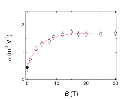
Fig. 5 shows the relation between and the applied magnetic field. The capacitance of the sample increases from the geometrical value 0.5 m-2 V -1 up to 1.8 m-2 V -1 at 9 T and saturates at this value for the highest fields. This effect is also observed implicitly in recent publications Feldman et al. (2009); Freitag et al. (2011) on high quality suspended bilayer-devices, but not mentioned by authors in the text.
As discussed in ref. Vera-Marun et al., 2011 the increase in capacitance of the system under applied magnetic field could be understood from the deviation from the flat-plate capacitor model. At the point when the width of the graphene flake is smaller or comparable to the distance to the back gate the flat-plate capacitor model can be no longer applied. The charge carrier distribution in graphene becomes non homogenous and increases at the edges. Since the classical cyclotron radius of charge carrier depends inversely on magnetic field, the increase of will cause edge channels in quantum Hall regime propagate closer to the edge, where the density can be few times higher than in bulk graphene. This would result an increase in capacitance extracted from QHE plateaus. The cyclotron radius is expected to be dependent on the charge carrier density as well. The exact calculations for different device’s geometries with charge carrier distribution in graphene, compared to the experiments, are the subject of another paper.Vera-Marun et al. (2011)
References
- Geim and Novoselov (2007) A. K. Geim and K. S. Novoselov, Nature Materials, 6, 183 (2007).
- Bolotin et al. (2008) K. I. Bolotin, K. J. Sikes, Z. Jiang, M. Klima, G. Fudenberg, J. Hone, P. Kim, and H. L. Stormer, Solid State Communications, 146, 351 (2008).
- Du et al. (2008) X. Du, I. Skachko, and E. Y. Andrei, International Journal of Modern Physics B, 22, 4579 (2008).
- Dean et al. (2010) C. R. Dean, A. F. Young, I. Meric, C. Lee, L. Wang, S. Sorgenfrei, K. Watanabe, T. Taniguchi, P. Kim, K. L. Shepard, and J. Hone, Nature Nanotechnology, 5, 722 (2010).
- Dean et al. (2011) C. R. Dean, A. F. Young, P. Cadden-Zimansky, L. Wang, H. Ren, K. Watanabe, T. Taniguchi, P. Kim, J. Hone, and K. L. Shepard, Nature Physics, 7, 693–696 (2011).
- Bolotin et al. (2011) K. I. Bolotin, F. Ghahari, M. D. Shulman, H. L. Stormer, and P. Kim, Nature, 475 (2011).
- Du et al. (2009) X. Du, I. Skachko, F. Duerr, A. Luican, and E. Y. Andrei, Nature, 462, 192 (2009).
- Feldman et al. (2009) B. E. Feldman, J. Martin, and A. Yacoby, Nature Physics, 5, 889 (2009).
- Tombros et al. (2011) N. Tombros, A. Veligura, J. Junesch, M. H. D. Guimaraes, I. J. Vera-Marun, H. T. Jonkman, and B. J. van Wees, Nature Physics, 7, 697 (2011a).
- Novoselov et al. (2006) K. S. Novoselov, E. McCann, S. V. Morozov, V. I. Fal/’ko, M. I. Katsnelson, U. Zeitler, D. Jiang, F. Schedin, and A. K. Geim, Nature Physics, 2, 177 (2006).
- Zhao et al. (2010) Y. Zhao, P. Cadden-Zimansky, Z. Jiang, and P. Kim, Physical Review Letters, 104, 066801 (2010).
- Nandkishore and Levitov (2010) R. Nandkishore and L. Levitov, Physical Review Letters, 104, 156803 (2010a).
- Nandkishore and Levitov (2010) R. Nandkishore and L. Levitov, Physical Review B, 82, 115431 (2010b).
- Zhang et al. (2011) F. Zhang, J. Jung, G. Fiete, Q. Niu, and A. H. MacDonald, arXiv:1010.4003v1 (2011).
- (15) J. Jung, F. Zhang, and A. H. MacDonald, Physical Review B, 83, 115408.
- (16) J. Martin, B. E. Feldman, R. T. Weitz, M. T. Allen, and A. Yacoby, Physical Review Letters, 105, 256806.
- Barlas et al. (2008) Y. Barlas, R. Cote, K. Nomura, and A. H. MacDonald, Physical Review Letters, 101, 097601 (2008).
- Tombros et al. (2011) N. Tombros, A. Veligura, J. Junesch, J. J. van den Berg, P. J. Zomer, M. Wojtaszek, I. J. V. Marun, H. T. Jonkman, and B. J. van Wees, Journal of Applied Physics, 109, 093702 (2011b).
- Novoselov et al. (2004) K. S. Novoselov, A. K. Geim, S. V. Morozov, D. Jiang, Y. Zhang, S. V. Dubonos, I. V. Grigorieva, and A. A. Firsov, Science, 306, 666 (2004).
- Blake et al. (2007) P. Blake, E. W. Hill, A. H. C. Neto, K. S. Novoselov, D. Jiang, R. Yang, T. J. Booth, and A. K. Geim, Applied Physics Letters, 91, 063124 (2007).
- Vera-Marun et al. (2011) I. J. Vera-Marun, P. J. Zomer, A. Veligura, M. H. D. Guimaraes, L. Visser, N. Tombros, H. J. van Elferen, U. Zeitler, and B. J. van Wees, (submitted to arxive) (2011).
- Moser et al. (2007) J. Moser, A. Barreiro, and A. Bachtold, Applied Physics Letters, 91, 163513 (2007).
- Abanin and Levitov (2008) D. A. Abanin and L. S. Levitov, Physical Review B, 78, 035416 (2008).
- Huard et al. (2008) B. Huard, N. Stander, J. A. Sulpizio, and D. Goldhaber-Gordon, Physical Review B, 78, 121402 (2008).
- Blake et al. (2009) P. Blake, R. Yang, S. V. Morozov, F. Schedin, L. A. Ponomarenko, A. A. Zhukov, R. R. Nair, I. V. Grigorieva, K. S. Novoselov, and A. K. Geim, Solid State Communications, 149, 1068 (2009).
- McCann (2006) E. McCann, Physical Review B, 74, 161403 (2006).
- Kim et al. (2011) S. Kim, K. Lee, and E. Tutuc, Physical Review Letters, 107, 016803 (2011).
- Veligura et al. (2012) A. Veligura, H.J. van Elferen, N. Tombros, J. C. Maan, U. Zeitler, and B. J. van Wees, arXiv:1202.1753 (2012).
- Kurganova et al. (2011) E. V. Kurganova, H. J. van Elferen, A. McCollam, L. A. Ponomarenko, K. S. Novoselov, A. Veligura, B. J. van Wees, J. C. Maan, and U. Zeitler, Physical Review B, 84, 121407 (2011).
- Wang et al. (2010) Z. Wang, L. Philippe, and J. Elias, Physical Review B, 81, 155405 (2010).
- Stormer et al. (1992) H. L. Stormer, K. W. Baldwin, L. N. Pfeiffer, and K. W. West, Solid State Communications, 84, 95 (1992).
- Lifshitz and Kosevich (1956) I. M. Lifshitz and A. M. Kosevich, Soviet Physics Jetp-Ussr, 2, 636 (1956).
- Kurganova et al. (2010) E. V. Kurganova, A. J. M. Giesbers, R. V. Gorbachev, A. K. Geim, K. S. Novoselov, J. C. Maan, and U. Zeitler, Solid State Communications, 150, 2209 (2010).
- Freitag et al. (2011) F. Freitag, J. Trbovic, M. Weiss, and C. Schönenberger, arXiv:1104.3816v2 (2011).