Bright single photon emission from a quantum dot in a circular Bragg grating microcavity
Abstract
Bright single photon emission from single quantum dots in suspended circular Bragg grating microcavities is demonstrated. This geometry has been designed to achieve efficient () single photon extraction into a near-Gaussian shaped far-field pattern, modest (10x) Purcell enhancement of the radiative rate, and a spectral bandwidth of a few nanometers. Measurements of fabricated devices show progress towards these goals, with collection efficiencies as high as demonstrated with moderate spectral bandwidth and rate enhancement. Photon correlation measurements are performed under above-bandgap excitation (pump wavelength = nm to nm) and confirm the single photon character of the collected emission. While the measured sources are all antibunched and dominantly composed of single photons, the multi-photon probability varies significantly. Devices exhibiting tradeoffs between collection efficiency, Purcell enhancement, and multi-photon probability are explored and the results are interpreted with the help of finite-difference time-domain simulations. Below-bandgap excitation resonant with higher states of the quantum dot and/or cavity (pump wavelength = nm to nm) shows a near-complete suppression of multi-photon events and may circumvent some of the aforementioned tradeoffs.
I Introduction
Single epitaxially-grown InxGa1-xAs quantum dots (QDs) have generated significant interest as potentially bright and stable single photon sources for quantum information processing applications [1, 2, 3]. In principle, the maximum achievable single photon rate is limited only by the spontaneous emission lifetime () of the QD, so that for a single InGaAs QD with a typical 1 ns in bulk, a single photon rate approaching 1 GHz may be possible. Still faster rates can be achieved through Purcell enhancement of the QD radiative rate [4]. In practice, however, the available single photon rates are not necessarily limited by the generation rate, but by the efficiency with which the single photons are funneled into a useful collection channel (e.g., low divergence angle far-field emission). This well-known problem [5, 6, 7] is fundamentally due to the high-refractive index contrast between the GaAs material in which the QD is embedded (refractive index ) and the surrounding air (=1). This strongly limits the amount of free-space emission exiting the semiconductor because of total internal reflection. Even with high numerical aperture (NA) optics, a maximum theoretical collection efficiency is expected.
This issue has been addressed by a number of groups. Solid immersion lenses [8, 9] provide a broadband and versatile approach to directly increase the collection efficiency. Alternatively, nanofabricated photonic structures such as optical microcavities [10, 11, 12] and waveguides[13, 14] provide confined or guided modes into which the QD can radiate. Ideally, the QD will dominantly radiate into a single mode of the structure (high spontaneous emission coupling factor ), which can then be efficiently out-coupled in the far-field depending on its emission pattern and divergence angle. Recent work [10, 13] has demonstrated efficiencies in excess of 50 into the first optical element of a fluorescence microscopy setup. The microcavity and waveguide approaches each offer their own advantages - microcavities supporting high quality factor () optical modes provide radiative rate enhancement, albeit over a narrow spectral band (the width of the cavity mode), while waveguides are broadband devices but typically do not offer rate enhancement (unless they operate in a slow-light regime). Broadband operation avoids the need for precise spectral alignment of the QD emission line to a photonic resonance and allows for efficient spectroscopy of multiple spectrally separated states of a single QD. On the other hand, radiative rate enhancement increases the maximum rate at which single photons can be generated by the QD, and can improve the indistinguishability of the photons [15, 16].
In ref. [17], we proposed and demonstrated a microcavity geometry for efficient extraction of photons from single QDs. This ’bullseye’ geometry, shown in Fig. 1, consists of a series of partially etched grooves in a suspended GaAs membrane containing a layer of InAs QDs. In comparison to many of the bright single photon geometries demonstrated thus far [11, 10, 13], which are based on vertically-oriented micropillars or nanowires, the bullseye geometry is planar, thereby requiring a relatively simple fabrication process. The fundamental optical mode of this cavity has a small volume , but a relatively low . This allows for both modest Purcell enhancement (maximum value 12 predicted in theory) and moderate spectral bandwidth (few nm for QDs emitting at nm). In addition, the geometry supports a far-field emission pattern that is near-Gaussian and predominantly directed vertically above the sample surface. Collection efficiencies higher than (for NA ) are predicted theoretically, and a measured efficiency of 10 was reported in ref. [17].
In this paper, we present further developments of the bullseye cavity, with a focus on better understanding its potential in single photon source applications. A key question left unanswered in ref. [17] is the degree to which multi-photon probability is suppressed in the out-coupled emission from the device, given the fact that the QD lines are situated on top of a broad cavity mode which also effectively out-couples other (non single photon) emission from multi-excitonic and hybridized QD-wetting layer states [18, 19]. Through photon correlation measurements of a series of devices under above-bandgap excitation (pump wavelength = nm to nm), we observe tradeoffs between collection efficiency, Purcell enhancement, and multi-photon probability. These tradeoffs, and the reduction in collection efficiency and Purcell enhancement relative to the maximum predicted values, are interpreted with the help of finite-difference time-domain simulations which focus on the role of variations in the grating geometry and QD position and orientation in influencing device performance. The results indicate that if adequate control of the QD position [20] and grating dimensions can be exercised, the device behavior may be tuned according to the application at hand (for example, limiting Purcell enhancement in exchange for single photon purity). Ideally, such tradeoffs would not be necessary, and as a first step towards improving this, we pursue below-bandgap excitation resonant with higher states of the QD and/or cavity (pump wavelength = nm to nm). These measurements show a near-complete suppression of multi-photon events and may circumvent some of the aforementioned limitations.
II Device Design
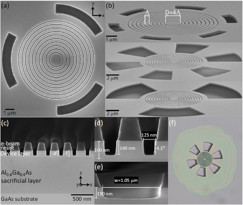
Our nanophotonic structure (Fig. 1) consists of a circular dielectric grating with radial period surrounding a central region of radius 2, produced on a suspended GaAs membrane. The GaAs slab of thickness supports single TE and TM polarized modes (electric or magnetic field parallel to the slab, respectively) at wavelengths near 980 nm. The grating is composed of partially etched circular trenches that have width , depth (), and are radially spaced by a period . Quantum dots are grown at the center of the GaAs membrane (), and are located randomly in the plane.
This ’bullseye’ geometry favors extraction of emission from QDs in the central circular region, which would otherwise be trapped inside the GaAs membrane. Indeed, a QD located in the central region radiates dominantly into slab-guided waves due to total internal reflection at the semiconductor-air interface. The role of the circular grating is to scatter such guided waves into free-space, preferentially upwards, towards the collection optic. Effective light extraction can be achieved via a second order Bragg grating for the slab modes (with period equal to the guided wave wavelength), which provides a first order diffraction perpendicular to the slab plane [21, 22]. In [22], linear gratings were developed to provide efficient coupling between free-space beams and planar waveguides modes. In our case, a circular grating geometry was a more natural choice because QD emission in the GaAs slab was expected to be cylindrically symmetric. We point out that similar circular geometries have been employed for enhanced light extraction from light emitting diodes [23], and for demonstrating annular Bragg lasers [24].
The grating period was chosen to approximately satisfy the second-order Bragg condition, , where is the GaAs slab TE mode effective index. Because this formula is valid in the limit of a weak grating, which is not the case here (as the grating’s etch depth is a considerable fraction of the slab thickness), we use it as a starting point in an optimization procedure which determines the correct period.
Partial reflections at the grating towards the center of the geometry lead to the formation of cavity resonances such as shown in Fig. 2(a), where the particular orientation of the cavity mode is determined by the orientation of the radiating dipole ( direction in this case). The large index contrast at the trenches leads to strong reflections and out-of-slab-plane scattering at the semiconductor-air interfaces, as apparent in Fig. 2(b). Resonances are centered at wavelengths determined by the radius of the central region and the grating geometry itself, which determines the overall phase of the reflected waves. Figure 2(c) shows the evolution of the resonance center wavelength for three varying grating periods . In addition to the trench spacing, large differences in propagation constants in the semiconductor and air regions of the grating produce significant resonance spectral shifts with small variations in trench width and depth.
The trench depth has a strong influence on the quality factor () and vertical light extraction, as incomplete spatial overlap between a trench and an incident slab-bound wave leads to both coupling to radiating waves and lower modal reflectivity. Preferential upwards vertical extraction results from the grating asymmetry, as evidenced in Fig. 2(c). This trade-off between the quality factor , power extraction and power extraction asymmetry, and far-field collimation due to variation in the trench depth is discussed further in Section IV-A. We note that our suspended, asymmetric grating approach limits radiation into the substrate without the need to oxidize the AlGaAs, bond the grating to a low index layer[24], or utilize a deeply etched geometry [10, 13].
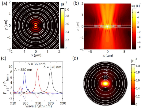
In Fig. 2(c), the maximum upwards extracted powers are ( is the emitted power for an electric dipole in a homogeneous GaAs medium), an indication of Purcell radiation rate enhancement due to the cavity [25, 26]. Indeed, for the nm structure the enhancement at the maximum extraction wavelength ( nm) is , where is the total radiated power in all directions. This resonance has , and its effective mode volume, calculated from the field distribution, is ( is the GaAs refractive index) [17]. Thus, despite the relatively low quality factor, the mode volume can be sufficiently small to produce a significant Purcell factor.
Finally, the far-field of the emitted radiation is highly directional, as evidenced in Fig. 2(d). Here, the emitted field for a dipole located at the bullseye center is nearly gaussian, and mostly contained within a half-angle. Indeed, in [17], we show that of the total emission can be collected with a NA=0.42 optic, while collection superior to 80 of the total emission can be achieved with NA. The dependence of the emitted field’s spatial distribution on geometric parameters is non-trivial, however, and is discussed further in Section IV-A.
Design Procedure
The design process used to generate Fig. 2 above and the results to be discussed in Section IV-A consisted of a series of finite-difference time-domain simulations that sought to maximize vertical light extraction near the QD’s expected s-shell emission ( nm), by varying , , and . The structures were excited with a horizontally oriented electric dipole at the bullseye center , representing an optimally placed QD. Total radiated power, steady-state upwards and downwards emission, and electromagnetic fields were then recorded at several wavelengths. The dipole orientation was assumed to be aligned along the plane, exciting only TE slab waves (self-assembled InAs QDs are expected to have electric dipole on the GaAs slab plane).
Steady-state fields at a surface just above the GaAs slab were used to calculate far-field patterns as in Fig. 2(d). The power collected by an optic of numerical aperture NA was calculated by integrating the far-field pattern over the appropriate angular range, and multiplying by the power radiated upwards.
III Experimental Results Under Above-Band Excitation
III-A Experimental Setup
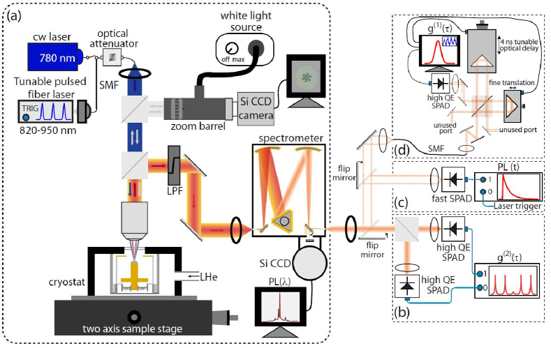
Figure 3 shows a detailed schematic view of several experimental setups used within this work. The sample was mounted on a cold finger and placed in a continuous flow liquid He cryostat that sits on a two-axis nano-positioning stage. Two different excitation sources were used to optically excite the QDs: (i) a CW laser diode ( nm) for above-band excitation, (ii) a tunable pulsed fiber laser ( nm to nm) for quasi-resonant excitation. Spectral properties of the QD emission were investigated via a low-temperature micro-photoluminescence (-PL) setup (Fig.3(a)), where a single microscope objective (NA = 0.42) was used for both the illumination of the sample and the collection of the emission. The collected signal is directed to a 500 mm focal length spectrometer either to record an emission spectrum with a Si Charge-Coupled Device (CCD) or to filter a single emission line for further investigations. For the second-order correlation function measurements, the spectrally filtered emission (with a linewidth pm 100 eV) is directed to a Hanbury-Brown and Twiss (HBT) type interferometer that consists of a 50/50 non-polarizing beamsplitter (NPBS) and two high quantum efficiency (QE) single-photon counting avalanche diodes (SPADs), as shown in Fig. 3(b). The SPADs (peak QE = 73 % at 700 nm and QE = 28 % at 980 nm) were connected to a time-correlated single-photon counting module to create a histogram of photon detection events. The dynamics of a single QD emission was measured by using a time-correlated single-photon counting (TCSPC) technique, which relies on measuring the time delay between an excitation pulse and detection of an emitted photon by using a fast SPAD (Fig. 3(c), timing jitter = 50 ps, QE = 3 % at 940 nm). Finally, for first-order field correlation function measurements, a Michelson interferometer was attached to the output of the spectrometer. As shown in Fig. 3(d), the setup consists of a 50/50 NPBS and two retro-reflectors, one of which is mounted on a linear stage to provide a coarse tunable optical delay up to 4 ns and the other retro-reflector is attached on a piezo actuator for a fine delay. The interference fringes were recorded by a SPAD, which was attached to one output port of the interferometer.
III-B Collection efficiency, time-resolved photoluminescence, and photon antibunching
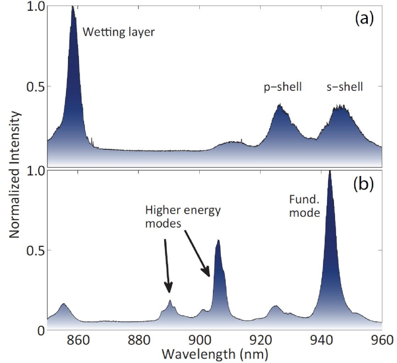
Initial characterization of the bare (unprocessed) QD sample has been done under strong pump powers with an excitation energy above the GaAs bandgap ( nm), which excites all QDs within the excitation spot. Figure 4(a) shows a low temperature wide range -PL spectrum of the QD ensemble, where clear s-shell and p-shell emission of the ensemble are observed around nm and nm, respectively. The sharper peak around nm is attributed to the wetting layer of the sample. In order to limit the number of QDs coupled to a mode, the bullseye devices are fabricated in a low QD density (1m-2) portion of the wafer and are designed to have their fundamental cavity mode spectrally aligned with the tail of the s-shell of the QD ensemble. We focus on three devices, named as BE1, BE2, and BE3, which have the same nominal grating period and central diameter , but differ due to slight variations in fabrication across the chip (trench width and depth) and perhaps most importantly, due to the varying QD location and orientation within the devices (which is random). Figure 4(b) shows a similar wide range high power -PL spectrum of device BE1, which clearly shows the fundamental mode (FM) and the well-separated higher energy modes of the cavity. The quality factor of the FM is measured from the ratio of the emission energy to the linewidth as = 200.
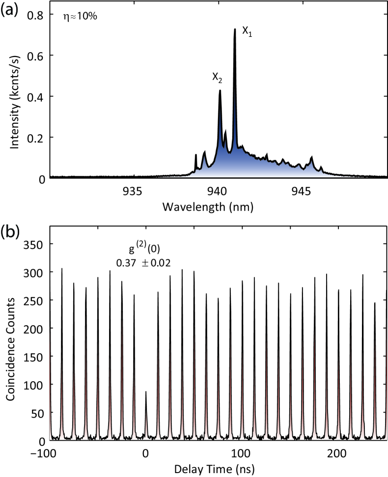
Figure 5(a) shows a low temperature (T = 10 K) -PL spectrum of BE1 taken under weak pulsed excitation of the GaAs ( nm). This device is the same as that presented in ref. [17], and displays bright emission lines labeled X1 and X2 that sit on top of a broad background due to the cavity mode emission, which is thought to be mainly fed by the multi-exciton states of several nearby QDs [18]. Both X1 and X2 emission lines have almost 10 collection efficiency at their saturation powers, and time-resolved PL measurements performed on the X1 line resulted in a lifetime as fast as 3606 ps, which is likely indicative of Purcell rate enhancement, as discussed later. In ref. [17], the characteristics of the X1 and X2 emission lines were investigated through pump-power-dependent and temperature-dependent PL measurements. Here, we focus on the single photon nature of the emission lines by measuring photon statistics through the HBT interferometer setup (Fig. 3(b)) under similar excitation conditions as in the previous work. Figure 5(b) shows the result of an intensity autocorrelation measurement performed on the spectrally filtered line at its saturation power. A clear suppression of the peak at zero time delay to a value of is seen [27], verifying that the measured line is originated from a single QD [2]. The deviation from the ideal value of for a single quantum emitter is most likely related to the uncorrelated background emission coupled to the cavity mode at the same frequency.
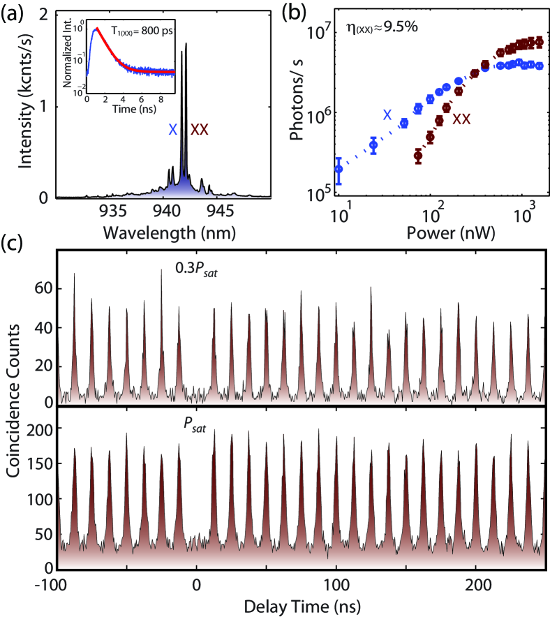
In Fig. 5, bright single photon generation from a single QD with a large collection efficiency and fast fluorescence decay time have been demonstrated. However, the autocorrelation measurements resulted in a clear background at the QD emission frequency due to contributions from other states resonant with the cavity mode emission. This suggests a potential trade-off between either (or both) high extraction efficiency and single photon purity of the collected signal or fast fluorescence decay time and purity of the collected signal. To further investigate this, two more devices (named as BE2 and BE3) were studied in detail. Figure 6(a) shows a low power emission spectrum of device BE2 taken under above-band pulsed excitation of the GaAs at T = 10 K. Similar to the device BE1, this device also shows two bright states named as excitonic (X) and bi-excitonic (XX) emission, which sit on top of the FM of the cavity around nm. Fig. 6(b) depicts the output intensity of X and XX emission lines as a function of excitation power in a double-logarithmic plot [28]. As is seen clearly, the X line has a linear power dependence while the XX line shows a quadratic increase with power as expected for exciton and bi-exciton emission from a single QD, respectively [29]. The output intensity of the X and XX emission lines in the figure are given as number of photons collected at the microscope objective, thus providing a direct estimate of total collection efficiency of the corresponding emission. Conversion of the integrated intensity of CCD counts to number of photons was done by measuring the total transmission of the optical path, as discussed in detail in the supplementary part of [17]. The extraction efficiency of exciton and bi-exciton emission are estimated as 5.4 and 9.5, respectively, by comparing the number of photons collected at the saturation power to the total number of photons generated from the corresponding emission line, assuming 100 radiative efficiency of the QD.
Having shown photon collection efficiencies on par with those seen in device BE1, we also performed autocorrelation measurements on the XX line under weak () and strong excitation powers (), the results of which are shown in Fig. 6(c). Almost complete suppression of the peak is observed even at the saturation power, yielding a great improvement compared to the results obtained from device BE1. The constant background observed in the autocorrelation measurements is mainly due to the overlap of broad correlation peaks indicating long lifetime of the measured emission. The inset of figure 6 (a) shows a direct measure of the lifetime of the XX emission through time-resolved PL setup. Applying an exponential fit to the measured decay curve gives the radiative lifetime as ps, slightly more than a factor of two larger than that measured for device BE1.
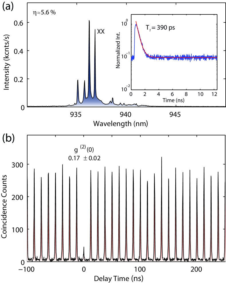
The results obtained from BE2 showed a clear improvement in the purity of the single photons generated from a single QD, with a cost of a longer radiative lifetime. A compromise between these two important parameters can also be achieved. Figure 7(a) shows a low temperature -PL spectrum of another device, named BE3, under weak pulsed excitation ( nm). Like the other devices, bright emission lines are visible on top of the cavity mode around nm, and are collected with an efficiency of at saturation (not shown). The inset of Fig.7(a) depicts the result of a time-revolved PL measurement performed on the XX line, which dominates the spectrum at elevated powers, and a radiative lifetime of about 39015 ps is estimated from the bi-exponential fit. This radiative lifetime is close to that measured for device BE1 and about a factor of two faster than that for BE2. In order to verify the single-photon nature of the measured emission line, an autocorrelation measurement was performed, the result of which is shown in Fig. 7(b). The reduced area of the peak at zero time delay indicates a clear photon antibunching with a value of , thus proving that the source is dominantly composed of single photons with a multi-photon probability in-between that of devices BE1 and BE2.
Devices BE1, BE2, and BE3 show radiative lifetimes of 360 ps, 800 ps, and 390 ps, indicating that the relative level of Purcell enhancement varies by a factor of 2.2 between the different devices. An estimate of the absolute Purcell enhancement factor requires a measurement of the QD lifetime without modification by the cavity. Unfortunately, the broad spectral bandwidth of the bullseye eliminates the potential for using temperature tuning to shift the QD lines off-resonance from the cavity. We instead measured the lifetime of QDs within suspended waveguides [14] made from the same wafer, where we saw characteristic lifetimes between 1.4 ns and 1.6 ns for the neutral exciton (X) state (no Purcell enhancement is expected in these devices). However, as described above, the lifetime and measurements for the bullseye devices were typically performed on the biexciton (XX) state, though we note that the collection efficiency of the exciton state was often equally as high. While the XX lifetime is in principle a factor of two times shorter than the X lifetime, other works [30, 31] have suggested that quantum confinement properties specific to the particular QD geometry may limit this reduction to a factor closer to 1.4. Taking this into account, we roughly estimate that a Purcell factor as high as 3 has been demonstrated in these devices.
III-C Coherence time
For quantum information processing applications, it is important not only to suppress multi-photon events but also to have the single photon wavepackets be indistinguishable [32, 16]. For an ideal transform-limited QD line, the coherence time would be twice the lifetime , and values approaching this limit have been demonstrated [33, 34]. In practice, achieving such coherence times depends strongly on parameters such as temperature and the method by which the QD is optically excited (e.g., above-band vs. resonant excitation).
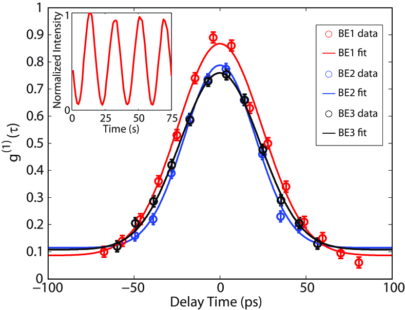
We investigate the coherence properties of the bright emission lines from all three bullseye devices by measuring the first-order field correlation function , which provides a direct access to the coherence time of the emission through [35]:
| (1) |
Experimentally, the function is measured from the visibility of the interference fringes observed at the output port of the Michelson interferometer (Fig. 3(d)) according to:
| (2) |
for equal intensities of interfered light. The inset to figure 8 shows an example of high-resolution interference fringes of the XX emission line from device BE1 obtained under above-band excitation conditions ( nm, CW). The visibility of the fringes at each systematically varied time delay between the interferometer arms are calculated according to Eqn. 2, and plotted in Fig. 8 for all devices [36]. The visibility of the interference fringes decreases with an increase in delay as a result of the limited coherence time of the emission. Applying a Gaussian fit to the visibility data reveals ps (eV) for BE1 and 17 ps (160 eV) for BE2 and BE3. The emission linewidth estimated from measurements is in full agreement with the linewidth obtained from the corresponding -PL spectrum for BE2 and BE3. However, the emission spectrum of device BE1 revealed a linewidth of 130 eV, which is broader than the linewidth obtained from measurement (100 eV). The difference mainly arises from the limited spectral resolution of the -PL setup estimated as 80 eV by measuring a narrow CW laser. The measured linewidths of emission from all devices are much broader than the reported homogenous linewidth of QDs that are nearly transform-limited (eV to 2 eV) [33, 34]. The main reason for this is thought to be the incoherent nature of the above-band excitation process, which excites several QDs within the excitation spot and thus enhances the dephasing processes due to the carrier-carrier interactions. In addition to that, spectral diffusion of the emission frequency due to fluctuating charges in the vicinity of the QDs may result in a broadening of the emission [37].
IV Discussion
The results presented above can be further interpreted with the help of numerical simulations. In particular, we try to understand how the specific device geometry influences the aforementioned trade-offs in different performance characteristics, as well as the reduced collection efficiency and rate enhancement observed in experiments relative to the maximum predicted theoretical values in ref. [17].
IV-A Tradeoffs in Purcell enhancement and collection efficiency
We next illustrate the effects of varying trench depths on emission properties of the circular dielectric grating. The first key quantity of interest is the Purcell enhancement factor . It is determined from simulation by the quantities and . is the total power emitted by a dipole in the bullseye structure, while is the power emitted by a dipole in a homogenous GaAs medium, so that is given by their ratio [25]. Figures 9(a) and (c) show as a function of wavelength and normalized trench depth . increases as approaches unity, with deeper trenches providing increased field confinement and higher cavity . This is a consequence of better overlap of the guided field inside the slab and the etched region, which leads to increased guided wave reflectivity and reduces coupling to out-of-plane radiation. The higher cavity with increasing trench depth is seen in the decreasing resonance width in Fig. 9(a); in addition, a strong blueshift of the cavity mode is observed.
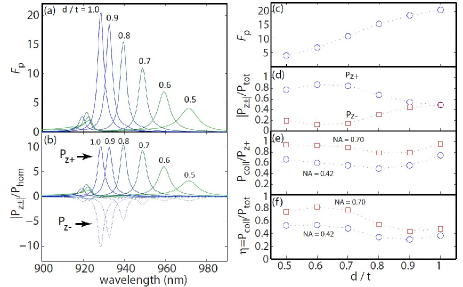
The increase in with trench depth comes at a cost, however, as the fraction of light emitted above the structure ( direction) is reduced. Intuitively, this makes sense in that, once the grating is completely symmetric (=1, for which is maximized), equal emission in the and directions should be expected. Figures 9(b) and (d) show the upwards () and downwards () extracted powers as a function of wavelength and normalized trench depth . Asymmetric and preferential upwards emission (determined by the ratio /) is maximized with , for which , but comes at the expense of a significantly reduced of 6.9 in comparison to its peak value of nearly 20.
For useful single photon emission, preferential upwards emission alone is not sufficient. We also require the emission to be directed within a relatively narrow divergence angle far-field pattern, so that the majority of this emission can be collected by a standard focusing optic. Figure 9(e) shows the fraction of upwards emission that is collected (/) by NA=0.42 and NA=0.7 optics, at the peak emission wavelength for each (see Fig. 9(a)). We note that this value is close to unity for the NA=0.7 optic, indicating a strong level of directionality, which we also expect based on the far-field emission pattern in Fig. 2(d). In addition, we see that the collection of the upwards-emitted power can vary by as much as 33 for the trench depth range considered. Finally, Fig. 9(f) shows the overall collection efficiency (=/) as a function of trench depth, which is the quantity that is actually measured in the experiments of the previous section. peaks at a value of 80 for a NA=0.7 optic, while for the NA=0.42 optic used in our experiments, this value is 50 .
It is evident from these results that sufficiently accurate control of the trench depth is a necessity, not only for optimal spectral alignment, but also for optimal extraction efficiency. For instance, for a trench depth , the collection efficiency into a 0.42 NA objective drops to approximately 34 % from the 53 % for . As nm, a 40 nm difference in trench depth, which we might expect to observe based on the tolerances of our fabrication process, can lower the maximum extraction efficiency significantly.
Along with radiative lifetime (determined by ) and collection efficiency, the third key characteristic of the devices measured in the previous section is the single photon purity (i.e., the value of ). Our simulations do not directly address the effects which cause . However, many works [18, 19] have attributed this to cavity-enhanced out-coupling of multi-excitonic and hybridized QD-wetting layer states that are spectrally resonant with the QD state of interest. In such a scenario, strongly Purcell-enhanced devices are likely to have levels that significantly differ from zero, while devices lacking Purcell enhancement can show even under above-band pumping near saturation [13]. From this, we speculate that shallower grating depths (), which lead to smaller in Fig. 10(c), may also lead to enhanced emission purity. Furthermore, this benefit would come together with increased collection efficiency (Fig. 10(f)) as a consequence of improved vertical extraction and emission asymmetry (Fig. 10(d)).
IV-B Influence of Dipole Position and Orientation
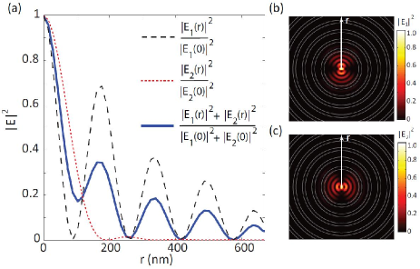
Other important factors affecting both the achieved Purcell radiative rate enhancement and overall photon collection efficiency are dipole position and orientation within the nanostructure. Considering the fundamental mode of the BE cavity in Fig. 2 (shown also in Fig. 10(b) and (c)), which we label as , we note that due to the circular symmetry of the nanostructure, both mode and a degenerate, 90∘ version of it (henceforth referred to as and , respectively) are simultaneously supported. Mode is exclusively excited by azimuthally oriented dipoles along the radial direction (), while mode is exclusively excited by radially oriented dipoles along . The specific instances of the modes excited by -polarized and -polarized dipoles are shown in Fig. 10(b) and (c), and a dipole oriented at an arbitrary angle in the plane would then be expected to radiate into both of these modes.
Figure 10(a) shows the intensities of and as functions of position along the radial direction (in this case, the direction), relative to those at the center. Since the radiative rate into a particular mode is proportional to the local modal electric field squared [25], it is apparent that Purcell radiative rate enhancement can vary significantly over very small position ranges, and also with dipole orientation. For a dipole with equal radial and azimuthal components, the plot of shown in Fig 10(a) makes it apparent that positioning within a nm radius from the center is necessary for maximal modal coupling and Purcell enhancement to be achieved.
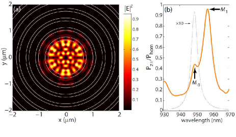
Coupling to both of the degenerate modes is not the only potential source of non-ideality for dipoles located away from the center of the cavity. Due to its large dimensions, the cavity supports not only the mode shown in Fig. 2(a) and (b), but also an ensemble of broad, spectrally overlapping resonances that can be excited by dipoles offset from the bullseye center. These resonances can have -factors comparable to that of the main mode (depending on the dipole location), however less directional far-fields. In this situation, an enhanced spontaneous emission rate can be achieved (with contributions from all modes), together with a reduced overall collection efficiency. To illustrate, we show in Fig. 11(a) the field profile of a high order mode that is excited on the same grating as in Fig. 2(a), when an -oriented dipole is placed at a distance of 260 nm away from the center. As shown in Fig. 11(b), this broad mode () is centered at 957 nm, and overlaps with the main cavity mode at 949 nm (compare with spectrum obtained for a centered dipole shown by the dotted line). The far-field of mode is such that only % of the total upwards radiated power can be collected by an NA=0.42 objective, significantly smaller than the % for . It is also worthwhile noticing in Fig. 11(b) that the radiative rates for both modes M0 and M1 for the offset dipole case are considerably lower than for a centered dipole (dotted line). This is expected because the modified radiative rate for a dipole in the nanostructure is proportional to , where is the electric field at the dipole position and for both modes the offset dipole is located near a null.
IV-C Quasi-Resonant Excitation
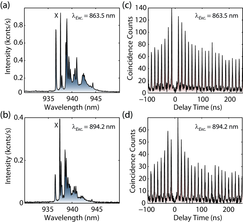
The coherence properties of single QD emission can be improved under selective excitation conditions, where the laser energy is tuned to a higher energy state of an individual QD. This so called ”quasi-resonant” excitation process limits the number of excited QDs, thus reducing the dephasing processes causing a linewidth broadening as mentioned before. Moreover, it also reduces the multi-photon generation probability significantly because of a reduced probability of creating more than one electron-hole pair in the QD. Figures 12(a) and (b) show emission spectra of device BE1 taken under quasi-resonant excitation, where the pulsed laser is tuned to 863.5 nm and 894.2 nm, respectively. In each spectrum, a bright excitonic emission line is visible at 937 nm, on which an autocorrelation measurement was also performed to investigate its single emitter nature. The result of the experiments are depicted in Figures 12 (c) and (d). A complete missing peak observed at zero time delay in both figures proves that the applied excitation scheme resulted in almost perfect single-photon generation from the measured emission line. An interesting feature seen in the figures is that the correlation peaks close to zero delay are much larger than the outer side peaks. Similar results were reported under quasi-resonant excitation of a single QD [38] and the observed blinking effect on a long time scale was attributed to a charge fluctuation of the QD. The linewidth of the measured state is extracted as eV from the corresponding -PL spectrum, which is narrower than the typical linewidths measured in -PL measurements under above-band excitation conditions.
V Conclusions
We have presented a series of measurements of single quantum dots in circular Bragg grating ’bullseye’ microcavities. These devices, first presented in ref. [17], offer a combination of features valuable to single photon sources: high extraction efficiency, moderate spectral bandwidth, and radiative rate enhancement, all within a planar geometry requiring a relatively straightforward fabrication procedure. Here, we focus on the tradeoff between rate enhancement and multi-photon probability present in these devices under above-band optical pumping. We first demonstrate that the brightest devices studied in ref. [17] indeed show antibunched photon statistics, but that the multi-photon probability is somewhat high (though still low enough that the source is dominantly comprised of single photons). We then consider two other devices in which the collection efficiency remains high, but the multi-photon probability is reduced, albeit at the expense of a longer radiative rate. We find that a near-complete suppression of multi-photon probability is possible in devices with high collection efficiency, but that the rate enhancement is correspondingly the lowest we see. These results suggest that unwanted background radiation (for instance, from transitions of multi-excitonic or hybrid quantum well-QD states) is enhanced and funneled through the cavity, leading to less pure single photon emission [18, 19]. Cavities with reduced Purcell enhancement may thus lead to reduced multi-photon emission [13].
Numerical simulations were performed to help interpret the physical scenarios that lead to the aforementioned compromises and the reduced collection efficiency and rate enhancement values observed relative to the maximum predicted values. The most straightforward method to improving the observed collection efficiency is through using an increased numerical aperture collection optic. Moving to an NA = 0.7 optic from the current NA = 0.42 optic is predicted to improve the collection efficiency for existing devices by 60 . Beyond this, precise control of the device geometry, both in terms of the etched trench depth and the QD position [20], are needed to achieve the desired combination of rate enhancement and collection efficiency. In particular, shallower grating trenches lead to increased light outcoupling, as well as a more highly asymmetric vertical emission, which ultimately leads to higher collection efficiencies. This comes at the cost of lower Purcell enhancement, which however may potentially lead to a more pure single photon emission, as discussed above.
Ideally, the bullseye cavity would be useful not only as a bright single photon source but as a bright source of indistinguishable single photons. Measurements under above-bandgap excitation indicate that the QD coherence time is extremely short ( 30 ps), so that quasi-resonant excitation [16, 34] or post emission spectral/temporal filtering [39, 40] will be required to generate indistinguishable photons. As a preliminary step towards this, we present photoluminescence spectra and photon correlation measurements of devices optically pumped at a wavelength resonant with higher states of the QD and/or cavity, for which near-complete suppression of multi-photon events is observed. Such quasi-resonant excitation may be an eventual route to simultaneously achieving high collection efficiency, strong rate enhancement, and suppressed multi-photon probability.
VI Acknowledgements
This work has been partly supported by the NIST-CNST/UMD-NanoCenter Cooperative Agreement. We thank Nick Bertone from OptoElectronic Components for loan of a high timing resolution single photon detector. The identification of any commercial product or trade name does not imply endorsement or recommendation by the National Institute of Standards and Technology.
References
- [1] A. J. Shields, “Semiconductor quantum light sources,” Nature Photonics, vol. 1, pp. 215–223, Apr. 2007.
- [2] P. Michler, A. Kiraz, C. Becher, W. V. Schoenfeld, P. M. Petroff, L. Zhang, E. Hu, and A. Imamoglu, “A Quantum Dot Single-Photon Turnstile Device,” Science, vol. 290, pp. 2282–2285, Dec. 2000.
- [3] C. Santori, M. Pelton, G. Solomon, Y. Dale, and Y. Yamamoto, “Triggered Single Photons from a Quantum Dot,” Phys. Rev. Lett., vol. 86, no. 8, pp. 1502–1505, Feb. 2001.
- [4] J.-M. Gérard and B. Gayral, “Strong Purcell effect for InAs quantum boxes in three-dimensional solid-state microcavities,” J. Lightwave Tech., vol. 17, no. 11, pp. 2089–2095, Nov. 1999.
- [5] H. Benisty, H. D. Neve, and C. Weisbuch, “Impact of Planar Microcavity Effects on Light Extraction - Part I: Basic Concepts and Analytical Trends,” IEEE J. Quan. Elec., vol. 34, no. 9, pp. 1612–1631, Sep. 1998.
- [6] W. L. Barnes, G. Bjrk, J. Gérard, P. Jonsson, J. A. E. Wasey, P. T. Worthing, and V. Zwiller, “Solid-state single photon sources: light collection strategies,” Eur. Phys. J. D, vol. 18, pp. 197–210, 2002.
- [7] J.-M. Gérard and B. Gayral, “Towards high-efficiency quantum-dot single photon sources,” Proceedings of SPIE, vol. 5361, pp. 88–95, 2004.
- [8] V. Zwiller and G. Bjork, “Improved light extraction from emitters in high refractive index materials using solid immersion lenses,” J. Appl. Phys., vol. 92, pp. 660–665, Jul. 2002.
- [9] A. N. Vamivakas, M. Atature, J. Dreiser, S. T. Yilmaz, A. Badolato, A. K. Swan, B. B. Goldberg, A. Imamoglu, and M. S. Unlu, “Strong extinction of a far-field laser beam by a single quantum dot,” Nano Letters, vol. 7, no. 9, pp. 2892–2896, 2007.
- [10] S. Strauf, N. G. Stoltz, M. T. Rakher, L. A. Coldren, P. M. Petroff, and D. Bouwmeester, “High-frequency single-photon source with polarization control,” Nature Photonics, vol. 1, pp. 704–708, Dec. 2007.
- [11] G. Solomon, M. Pelton, and Y. Yamamoto, “Single-mode spontaneous emission from a single quantum dot in a three-dimensional microcavity,” Phys. Rev. Lett., vol. 86, no. 17, pp. 3903–3906, 2001.
- [12] M. Toishi, D. Englund, A. Faraon, and J. Vuckovic, “High-brightness single photon source from a quantum dot in a directional-emission nanocavity,” Opt. Express, vol. 17, no. 7, pp. 14 618–14 626, 2009.
- [13] J. Claudon, J. Bleuse, N. S. Malik, M. Bazin, P. Jaffrennou, N. Gregersen, C. Sauvan, P. Lalanne, and J. Gérard, “A highly efficient single-photon source based on a quantum dot in a photonic nanowire,” Nature Photonics, vol. 4, pp. 174–177, Mar. 2010.
- [14] M. Davanço, M. T. Rakher, , W. Wegscheider, D. Schuh, A. Badolato, and K. Srinivasan, “Efficient quantum dot single photon extraction into an optical fiber using a nanophotonic directional coupler,” Appl. Phys. Lett., vol. 99, p. 121101, 2011.
- [15] S. Varoutsis, S. Laurent, P. Kramper, A. Lemaître, I. Sagnes, I. Robert-Philip, and I. Abram, “Restoration of photon indistinguishability in the emission of a semiconductor quantum dot,” Phys. Rev. B, vol. 72, no. 4, p. 041303, Jul 2005.
- [16] C. Santori, D. Fattal, J. Vuckovic, G. Solomon, and Y. Yamamoto, “Indistinguishable photons from a single-photon device,” Nature, vol. 419, pp. 594–597, Oct. 2002.
- [17] M. Davanço, M. T. Rakher, D. Schuh, A. Badolato, and K. Srinivasan, “A circular dielectric grating for vertical extraction of single quantum dot emission,” Appl. Phys. Lett., vol. 99, p. 041102, 2011.
- [18] M. Winger, T. Volz, G. Tarel, S. Portolan, A. Badolato, K. Hennessy, E. L. Hu, A. Beveratos, J. Finley, V. Savona, and A. Imamoglu, “Explanation of Photon Correlations in the Far-Off-Resonance Optical Emission from a Quantum - Dot Cavity System,” Phys. Rev. Lett., vol. 103, p. 207403, 2009.
- [19] A. Laucht, M. Kaniber, A. Mohtashami, N. Hauke, M. Michler, and J. Finley, “Temporal monitoring of nonresonant feeding of semiconductor nanocavity modes by quantum dot multiexciton transitions,” Phys. Rev. B, vol. 81, p. 241302, Jun 2010.
- [20] K. Hennessy, A. Badolato, M. Winger, D. Gerace, M. Atature, S. Guide, S. Falt, E. Hu, and A. Imamoglu, “Quantum nature of a strongly coupled single quantum dot-cavity system,” Nature (London), vol. 445, pp. 896–899, Feb. 2007.
- [21] A. Hardy, D. Welch, and W. Streifer, “Analysis of second-order gratings,” Quantum Electronics, IEEE Journal of, vol. 25, no. 10, pp. 2096 –2105, oct 1989.
- [22] D. Taillaert, W. Bogaerts, P. Bienstman, T. F. Krauss, P. V. Daele, I. Moerman, S. Vertuyft, K. D. Mesel, and R. Baets, “An Out-of-Plane Grating Coupler for Efficient Butt-Coupling Between Compact Panar Waveguides and Single-Mode Fibers,” IEEE J. Quan. Elec., vol. 38, no. 7, pp. 949–955, Jul. 2002.
- [23] M. Y. Su and R. P. Mirin, “Enhanced light extraction from circular bragg grating coupled microcavities,” Applied Physics Letters, vol. 89, no. 3, p. 033105, 2006.
- [24] W. M. J. Green, J. Scheuer, G. DeRose, and A. Yariv, “Vertically emitting annular Bragg lasers using polymer epitaxial transfer,” Appl. Phys. Lett., vol. 85, no. 17, pp. 3669–3671, Oct. 2004.
- [25] Y. Xu, J. S. Vučković, R. K. Lee, O. J. Painter, A. Scherer, and A. Yariv, “Finite-difference time-domain calculation of spontaneous emission lifetime in a microcavity,” J. Opt. Soc. Am. B, vol. 16, no. 3, pp. 465–474, 1999.
- [26] J. Vučković, O. Painter, Y. Xu, A. Yariv, and A. Scherer, “FDTD Calculation of the Spontaneous Emission Coupling Factor in Optical Microcavities,” IEEE J. Quan. Elec., vol. 35, no. 8, pp. 1168–1175, Aug. 1999.
- [27] The value is determined by comparing the integrated area of the peak around time zero to the average area of the peaks away from time zero. The uncertainty on this value is given by the standard deviation in the area of the peaks away from time zero.
- [28] The photon count rate vs. pump power plot in Fig. 6(b) is determined by fitting the spectral peak to a Lorentzian and integrating the area within the Lorentzian. Error bars are due to the uncertainty of the fit and are one standard deviation in amplitude.
- [29] R. M. Thompson, R. M. Stevenson, A. J. Shields, I. Farrer, C. J. Lobo, D. A. Ritchie, M. L. Leadbeater, and M. Pepper, “Single-photon emission from exciton complexes in individual quantum dots,” Phys. Rev. B, vol. 64, p. 201302(R), 2002.
- [30] C. Santori, G. S. Solomon, M. Pelton, and Y. Yamamoto, “Time-resolved spectroscopy of multiexcitonic decay in an InAs quantum dot,” Phys. Rev. B, vol. 65, p. 073310, Feb. 2002.
- [31] A. Kiraz, S. Falth, C. Becher, B. Gayral, W. V. Schoenfeld, P. M. Petroff, L. Zhang, E. Hu, and A. Imamoglu, “Photon correlation spectroscopy of a single quantum dot,” Phys. Rev. B, vol. 65, p. 161303, Mar. 2002.
- [32] A. Kiraz, M. Atature, and A. Imamoglu, “Quantum-dot single-photon sources: Prospects for applications in linear optics quantum-information processing,” Phys. Rev. A, vol. 69, p. 032305, 2004.
- [33] M. Bayer and A. Forchel, “Temperature dependence of the exciton homogeneous linewidth in self-assembled quantum dots,” Phys. Rev. B, vol. 65, p. 041308(R), 2002.
- [34] S. Ates, S. M. Ulrich, S. Reitzenstein, A. Löffler, A. Forchel, and P. Michler, “Post-selected indistinguishable photons from the resonance fluorescence of a single quantum dot in a microcavity,” Phys. Rev. Lett., vol. 103, no. 16, p. 167402, Oct 2009.
- [35] R. Loudon, The Quantum Theory of Light, 3rd ed. Oxford University Press, 2000.
- [36] The error bars in the data in Fig. 8 are determined by the fluctuations in the inteference contrast and are one standard deviation in amplitude.
- [37] J. Seufert, R. Weigand, G. Bacher, T. Kümmell, A. Forchel, K. Leonardi, and D. Hommel, “Spectral diffusion of the exciton transition in a single self-organized quantum dot,” Appl. Phys. Lett., vol. 76, p. 1872, 2000.
- [38] C. Santori, D. Fattal, J. Vuckovic, G. S. Solomon, E. Waks, and Y. Yamamoto, “Submicrosecond correlations in photoluminescence from InAs quantum dots,” Phys. Rev. B, vol. 69, p. 205324, May 2004.
- [39] R. B. Patel, A. J. Bennett, K. Cooper, P. Atkinson, C. A. Nicoll, D. A. Ritchie, and A. J. Shields, “Postselective two-photon interference from a continuous nonclassical stream of photons emitted by a quantum dot,” Phys. Rev. Lett., vol. 100, no. 20, p. 207405, May 2008.
- [40] M. T. Rakher and K. Srinivasan, “Subnanosecond electro-optic modulation of triggered single photons from a quantum dot,” Appl. Phys. Lett., vol. 98, no. 21, p. 211103, May 2011.