Metal Cluster’s Effect on the Optical Properties of Cesium Bromide Thin Films
Abstract
Cesium Bromide films grown of glass substrates by thermal evaporation showed interesting optical properties. The UV-visible absorption spectra showed peaks which showed red shift with time. Structural and morphological studies suggested decrease in grain size with time which was unusual. Theoretical simulation shows the optical behaviour to be due to surface plasmon resonance resulting from Cesium clyindrical rods embedded in the films.
PAC No: 68.55.-a, 71.20.Ps, 78.67.Bf
Keywords: Alkali halides, Thin Films, X-Ray Diffraction,
UV-visible spectroscopy
1 Introduction
Alkali Halides (AH) have been extensively studied in the early years to understand the variation in energy band structure with changing lattice constant [1]. The simple cubic crystal structures, experimentally determinable phase transitions and variation in properties when these samples are subjected to presure made them popular samples [2]. Also, AH are highly photon-absorbing materials in X-ray and Ultraviolet region, giving rise to color-centers [3]-[6]. Cesium halides hence became popular in detectors and optoelectronics devices [7]. Cesium halides also showed excellent quantum efficiency. Infact, thin CsBr films deposited on thin metal layers have useful application as electron source and as protective layer of photocathode [8]. However, AH films suffered due to their high reactivity with atmospheric water vapor [9] making it difficult to maintain. In this manuscript we focus on Cesium Bromide, since of all the alkali halides, it exhibits a relatively higher stability when exposure in air [10].
Recent interest in Alkali Halides is due to the appearance of Surface Plasmon Resonance (SPR) peaks in the UV-visible region of its absorption spectrum, when noble and other metal nano-particle are embedded in it [11]. However, we have noticed SPR peaks developing in cesium iodide [12] and cesium bromide (present work) thin films even with aging. We believe this to be a direct proof of the idea put forward by Emel’yanov and others [13, 14]. They claimed that the defect (such as F-centers) in alkali halides when provided the right conditions would lead to metal cluster formations. We believe it is these alkali clusters that form the metal nanoparticles responsible for SPR formation. In the present work we report formation of Cesium cluster in CsBr thin films due to ageing effect and their effect on optical properties.
2 Experimental
Cesium Bromide thin films were deposited by thermal evaporation on microscopy glass substrates. The starting material (powder) was obtained from HiMedia (Mumbai) and was of 99.98% purity. Films depositons were carried out at room temperature with vacuum better than Torr. The thickness of the films were monitered with the help of a Digital Thickness Moniter (DTM-106). One part of the films were kept in desiccators and taken out only for characterization while the second part were kept outside, exposed to open air. This was done to compare the ageing effect of these films maintained in different conditions.
The structural and optical characterization the samples were done with Philips PW 3020 diffractometer and Systronics double beam UV-visible spectrophotometer (2202). Surface morphology and elemental composition of films were examined with Field-Emission Scaning Electron Microscopy (FE-SEM) FEI-Quanta 200F and the Energy Dispersive Analysis of X-rays (EDX) system attached with it.
3 Results and Discussion
3.1 Optical Studies
The absorption spectra of Cesium Bromide films showed thickness dependence with films thicker than 550 nm showing intense absorbance in the visible region. We believe that these peaks are due to surface plasmon resonance (SPR). SPR peaks results from the interaction between metal conduction electron and the electric field component of incident electromagnetic radiation [15]. This interaction leads to collective oscillations of free electrons on the metal surface if the metal particle’s dimensions are smaller than or comparable to the incident wavelength of light. These peaks in CsBr’s absorbance spectra are a result of metal nano-clusters of cesium existing within the films. Studies on Cesium Iodide too had revealed similar peaks in their UV-visible absorption spectra in our earlier studies [12].
However, what is intrigging in Cesium Bromide is the systematic variation in film property with time. UV-visible spectra recorded immediately after film fabrication showed a dominant peak around 500 nm. Not only did this peak red-shift with time but also its absorption intensity was also found to decrease. The UV-visible absorption spectra (Fig 1) of a 840 nm thick sample taken at various intervals after film fabrication exhibits this trend. This ageing effect of the sample is believed to depend on the ambient atmosphere in which the sample was maintained, hence as explained above, one set of the samples were maintained in a dessicator while the second set were maintained in a normal miscroscope slide box. As expected, both samples that started with identical UV-visible spectra showed different rate of variation. Those kept in dessicator aged slower. The shift in peak position shows a linear trend with time and the rate of change was found to be film thickness dependent (fig 2a). Thicker films showed higher rate of shift as compared to the thinner films (fig 2b). Even the decrease in absorption showed systematic trend of variation with time (fig 2c).
Both the SPR peak position and its intensity are strongly dependent on the metal cluster’s size, it’s and that of the surrounding media dielectric constant. These results, hence, indicate some systematic and continuous changes in the film that require investigation. Below we focus our attention on how metal clusters arise in our samples and the structural and morphological changes which would explain the variations observed.
3.2 Morphological, Structural & Compositional Studies
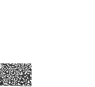
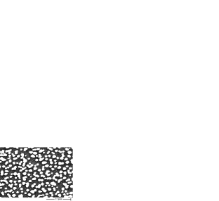
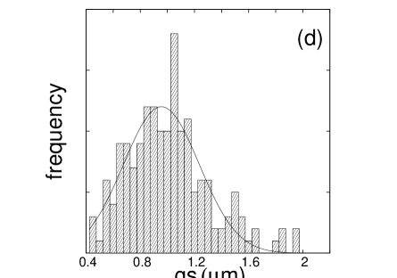
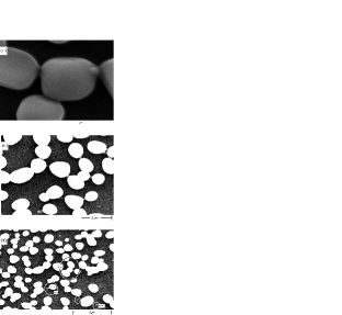
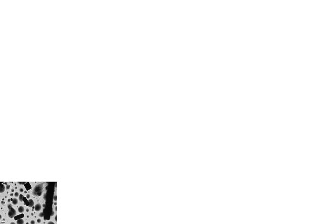
As can be seen from fig 3, sharp edged grains can be found uniformally scattered on the film surface. The micrographs of this figure compares two samples, (a) sample maintained in dessicator and (b) that kept outside. The grain density and grain size were determined from these micrographs using the software ImageJ. Below each micrograph histograms depicting the grain size distribution in the micrograph are given. As can be seen, samples kept in dessicator showed slightly larger grains in the sample maintained in the dessicator as compared to that maintained outside ( as compared to ). The grain density of samples kept in air () was found to be nearly twice that of the counterpart kept in the dessicator (). The full width at half maxima (FWHM) of the Guassian fit to the histograms also reflect a narrower distribution for the samples maintained in the dessicator. Viewed in conjucture these results suggest grains of the film split giving rise to smaller grains. Also, this process of grain breaking is encouraged in samples kept in air. Figure 4 gives a suggestive sequence of “grain division”. Fig 4a shows two grains in close proximity that are inter-connected by vesticles. These structures increase in length as the grains move apart. As the grains moves apart, the vesticle like structure is retained by one of the grains (see fig 4b). These vesticles finally break off and fall into the background (circles marked in fig 4c highlight this) leaving behind a smooth spherical grain. EDX (Table 1) on vesticle and grains show them to be made up of cesium and cesium bromide respectively. These results would indicate removal of bromide from the surfaces of the grains. The process is accelerated in the samples kept in air. The sublimation leaves behind cesium metal layer on the surface of the grain, resulting in a “insulator-metal” “core-shell” structure. Figure 5 is a sample TEM micrograph which clearly shows distinct regions of core and shell. As expected there is a large variation in the grain size. Also, seen distributed among the spherical shells are “rod” like structures we have explained above.
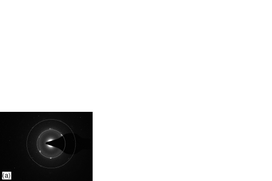
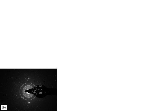
Fig 6(a) shows the Selected Area Electron Diffraction (SAED) taken on one of the core of the “core-shell” grains. The spots indicate the crystalline nature of the “core”. The major spots of the SAED are arranged on thwo distinct rings corresponding to the (110) and (211) peaks of CsBr as indexed in ASTM Card No 73-0391. Similar analysis of the rod region (fig 6b) shows it to be crystalline with three distinct ring corresponding to the (200), (331) and (220) planes of Cesium as given in the ASTM Card No 18-0325.
X-ray Diffraction of the samples shows two major peaks of CsBr. The existence of both CsBr and Cs in our samples are confimred by the broad peaks at and (fig 7). These peak positions match those given in ASTM Card No 73-0391 and 18-0325. The grain sizes (Table 2) of CsBr core were also calculated from the X-ray diffraction (fig 7) peak’s Full Width at Half Maxima (FWHM) using Scherrer formula [16]. The smaller grain sizes indicate that the grain boundaries of the core, as viewed in the micrographs, enclose crystalline region along with amorphous CsBr. While the amount of free Cesium in the samples can be thought to be low, X-Ray diffraction pattern does show a broad peak at , formed by merging of the (211) and (220) peaks of CsBr and Cs. On deconvoluting these peaks, the average grain size of free Cesium were also calculated. Grain size of CsBr and Cs were found to decrease with increasing time. This trend is in agreement with those from morphological studies. However, more importantly, the CsBr peaks were found to have shifted to the right as compared to the peak positions given in the ASTM Card. This would indicate that the CsBr lattices are in a state of stress with compressive forces acting on it. The stress in the film were calculated after evaluating the strain using the relation [17]
| (1) |
where is the experimentally observed d-spacing and is the corresponding peak’s d-spacing as reported in the ASTM card. The stress then is determined by multiplying the strain by the elastic constant of the material. The calculated strain on the (110) plane of CsBr changed from -0.0023 to -0.0028 with an elapse of 900 hours. We believe it is this stress that contributes to the required energy for bromide’s disassociation.
3.3 Theoretical Modeling
Metal-insulator core-shell structures and nano-rods are known to give rise to SPR peaks in absorbance spectra in the visible and near IR region [18, 19]. As stated earlier, the SPR peak position and intensity strongly depend on the metal cluster size, shape, its dielectric constant and that of the surrounding. Since, the surrounding of the metal clusters in this study is invariant (CsBr), we may use the results here to investigate the contribution of size, shape and cesium’s dielectric constant in SPR’s peak position. The systematic variation in SPR peaks (fig 1 and fig 2) indicate a systematic variation in one of the mentioned properties.
The TEM micrograph (fig 5) shows existence of both cylinderical or nano-rod structures along with spherical core-shell structures in out sample. Hence, it becomes important to isolate which of these structures contribute to the SPR peaks in the wavelength region of 500-600nm. This can be done using the theoretical framework given by Mie [20] to explain the scattering and absorption caused by metal clusters. The Mie theory essential is an application of Maxwell’s equation for electromagnetic plane waves incident on metal particles. Recent works by Balaji et al [21] extends Mie theory to explain scattering and absorption by core-shell structures. We have extended those calculation schemes on our Cesium Bromide-Cesium core-shell structures and find theoretically for the grain diamensions that exist in our samples, there are no or very shallow peaks in the visible region (fig 8). For the same aspect ratio () but decreasing grain size, we see a blue shift in the shallow peak observed. This is not in agreement with our experimental observations of fig 1.
As for theoretically calculating the SPR extinction cross-section of nano-spherical clusters, the Gans theory [22] is both simple and accurate and is given as [23]
| (2) |
where and are the real and imaginary part of the metal nanocluster’s dielectric constant and the dielectric constant of the media in which the metal nano-clusters are embedded in. The depolarising factors [24] can be easily modified for cylinderically shaped clusters by taking the aspect ratio (c/a) to be far less than unity [25]. Figure 9 shows the extinction cross-sections calculated for decreasing average grain size but increasing aspect ratio. For the calculations here, we have used the frequency dependent dielectric coefficients reported by [26]. The curves and the trend are in agreement with the the experimental trends shown in figure 1.
For completeness, we used eqn (2) to see the shift in SPR peak position with varying . This gives the SPR sensitivity to the medium’s refractive index [27]. Based on our calculations we find the slope between SPR peak position and medium’s refractive index to be 145.1 nm/RIU (fig 10). This small slope would in turn demand Cesium Bromide’s refractive index to change from 1.66 to values greater than 4.10 to explain the results of fig 2(a). Thus, we conclude that the variation of optical properties seen with ageing in the Cesium Bromide films can be explained based on basis of formation of Cesium nano-rods in it.
4 Conclusions
Experimental data suggests that the stress in the as grown films lead to formation of defects caused by Bromide atom’s displacement. These defects start collecting together to form clusters. With the curvature of the grain’s surfaces contributing the maximum stress, the formation of Cesium at the grain surfaces can be understood. This surface Cesium around Cesium Bromide not only contributes to the core-shell structures present in the film but also the a site for formation of Cesium nano-rods. With time the shell-core grain size decreases along with decrease in the average grain size of the cylinderical rods. Comparing the results with theoretical simulations suggests cylinderical grains contribute to SPR peaks in the visible wavelengths with decreasing grain size accompanied with increasing aspect ratio (ratio of diameter to length) leading to a red-shift in the peak position.
Acknowledgment
The authors would like to express their sincere gratitude to Department of Science and Technology (DST) India for the financial assitance (SR/NM.NS-28/2010) given for carrying out this work.
Tables
Table 1: Compares the presence of various elements (given in weight
percent) in the grain and vesticles in in the electron micrographs. The
chemical composition as measured using EDX attachment with the SEM.
| Element | CsBr (at grain) | CsBr (at vesticle) |
|---|---|---|
| CK | 18.04 | 49.58 |
| OK | 15.72 | 22.29 |
| MgK | 02.08 | 01.45 |
| SiK | 20.85 | 19.70 |
| CaK | 03.35 | 03.49 |
| CsL | 17.66 | 03.50 |
| BrK | 22.30 | 00.00 |
Table 2: Grain size (gs) of CsBr and Cs as calculated from the X-Ray
Diffraction Pattern.
| Time (Hrs) | gs of CsBr (nm) | gs of Cs (nm) |
| 22 | 65 | 88 |
| 112 | 55 | 76 |
| 794 | 58 | 10 |
| 1034 | 34 | – |
References
- [1] H. Fujita, K. Yamauchi, A. Akasaka, H. Irie and S. Masunaga, J. Phys. Soc. Japan, 68 (1999) 1994.
- [2] M.B.Nardelli, S. Baroni and P. Giannozzi, Phys. Rev. B, 51 (1995) 8060.
- [3] P.V. Mitchell, D. A. Wiegand and R. Simoluchowski, Phys. Rev., 121 (1961) 484.
- [4] F.T. Goldstein, Phys. Stat. Solidi (B), 20 (1967) 379.
- [5] M. Elango, Christian Gahwiller, F.C. Brown, Soid State Comm., 8 (1970) 893.
- [6] B.R. Sever, N. Kristianpollar and F.C. Brown, Phys. Rev. B, 34 (1986) 1257.
- [7] D.B. Sirdeshmukh, L. Sirdeshmukh and K.G. Subhadra, “Alkali Halides, A Hnadbook of Physical Properties”, (Springer, Berlin 2001).
- [8] A. Brakin, Nucl. Instrum. Methods Phys. Res. A, 367, 325 (1995).
- [9] G. Yoshikawa, M. Kiguchi, K. Ueno, A. Saiki, Surf. Sci., 554 (2003) 220.
- [10] Ed. W.M. Haynes, “CRC Handbook of Chemistry and Physics”, (CRC Press, USA 2011).
- [11] S. Nie and S.R. Emory, Science, 275 (1997) 1102.
- [12] K. Kumar, P. Arun, C. R. Kant, N.C. Mehra and V. Methew, Appl. Phys. A, 99 (2010) 305.
- [13] V.I. Emel’yanov, Laser Phys., 2 (1992) 389.
- [14] S. Seaglione, R.M. Montereali, V. Mussi and E. Nichelatti, J. Optoelect. Adv. ¡ater. 7 (2005) 207.
- [15] U. Kreibig and M. Vollmer, “Optical Properties of Metal Clusters”, (Springer, Berlin, 1995).
- [16] B.D. Cullity, “Elements of X-ray diffraction” (2ndEd, Addisson-Wesley, NY).
- [17] A.L. Patterson, Phys. Rev., 56 (1939) 978.
- [18] J. Perez-Juste, I. Pastoriza-Santos, L.M. Liz-Marzan and P. Mulvaney, Coordination Chem Rev., 249 (2005) 1870.
- [19] C.F. Bohren, D.R. Huffman, “Absorption and Scattering of Light by Small Particles” (John-Wiley & Sons, NY, 1983).
- [20] G. Mie, Ann. Phys, 25 (1908) 329.
- [21] B. K. Juluri, Y. B. Zheng, D. Ahmed, L. Jenson and T.J. Hung, J. Phys. Chem C, 112 (2008) 7309.
- [22] R. Gans, Ann. Phys., 47 (1915) 270.
- [23] S. Link, M. Mohamed, M. El-Sayed, J. Phys. Chem. B, 103 (1999) 3073.
- [24] C. Noguez, J. Phys. Chem. C, 111 (2007) 3086.
- [25] A. Burchanti, A. Bogi, C. Marinelli, C. Maibohm, E. Mariotti, S. Sanguinetti, L. Moi, Eur. Phys. J. D, 49 (2008) 201.
- [26] N.V. Smith, Phys. Rev. B, 2 (1970) 2840.
- [27] H. Chen, L. Shao, K. C. Woo, T. Ming, H. Lin and J. Wang, J. Phys. Chem. C, 113 (2009) 17691.
Figure Captions
-
Fig 1
The Absorbance spectra of a representative sample (not kept in dessicator) taken at various intervals. Interestingly, as the SPR’s peak position shifted to higher wavelengths, the intensity showed presistent decrease. The SPR’s peak position’s shift to higher wavelengths with time show a linear trend.
-
Fig 2
The Absorbance spectra of three different CsBr films varying by thickness show systematic variation with time. (A) The peak position varies linearly with time, where the (B) slope (rate at which peak position varies with time) is directly dependent on film thickness. (C) shows the absorption intensity also varies with time.
-
Fig 3
Field-Emission Scanning Electron Microscope (SEM) micrographs of (a) sample maintained in dessicator and (b) kept outside. Histograms (c) and (d) shows the grain size (gs) distribution of sample maintained in dessicator and those kept outside, respectively.
-
Fig 4
Field-Emission Scanning Electron Microscope images show the sequence of events as CsBr grains break away. Micrograph (a) shows “vesticles” of Cesium inter-connecting grains which (b) break away with “vesticle” going with one of the grains. These “vesticles” fall off (c) giving cesium rods in the film.
-
Fig 5
Transmission Electron Microscope (TEM) images confirm nature of film throughout the thickness of the film is same as that seen on the surface using SEM.
-
Fig 6
Surface Analysis using Electron Diffraction (SAED) of (a) the core and (b) the rod.
-
Fig 7
X-Ray diffraction of CsBr films after aging. Both broad peaks are deconvoluted to show the Cs () and CsBr ().
-
Fig 8
Extinction cross-section of Cesium Bromide-Cesium core-shell structure calculated (see text) for two different grain sizes, namely (a) 1500 and (b) 1200nm, but same aspect ratio ().
-
Fig 8
Theoretically projected variation of SPR peaks caused by Cesium nano-rods. Family of curves show a redshift with average grain size decreasing abid increasing aspect ratio (c/a). The calculations where made using Gans Model (see text). The simulation follow the same trands of fig 1.
-
Fig 10
Graph shows the relationship between SPR peak position with surrounding media’s refractive index.
Figures