First-Principles Modeling of Pt/LaAlO3/SrTiO3 Capacitors
Under an External Bias Potential
Abstract
We study the electrical properties of Pt/LaAlO3/SrTiO3 capacitors under the action of an external bias potential, using first-principles simulations performed at constrained electric displacement field. A complete set of band diagrams, together with the relevant electrical characteristics (capacitance and built-in fields), are determined as a function of LaAlO3 thickness and the applied potential. We find that the internal field in LaAlO3 monotonically decreases with increasing thickness; hence, the occurrence of spontaneous Zener tunneling is ruled out in this system. We discuss the implications of our results in the light of recent experimental observations on biased LaAlO3/SrTiO3 junctions involving metallic top electrodes.
pacs:
73.20.-r, 71.15.-m, 71.70.-d
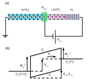
In recent years oxide-oxide heterojunctions have generated widespread interest, because of their potential for applications in microelectronics and intriguing fundamental physics. When thin films of polar LaAlO3 (LAO), composed of formally charged (LaO)+ and (AlO2)- layers, are stacked on top of the non-polar surface of SrTiO3 (STO), a two-dimensional metallic electron gas appears at the interface under suitable experimental conditions ohtomo04 . In particular, TiO2-terminated LAO/STO interfaces are found to undergo an insulating-to-conducting transition (named “electronic reconstruction”) when the thickness of the LAO film exceeds layers thiel06 . Alternatively, 2D metallicity can be switched on and off by applying an external bias potential between the conducting LAO/STO interface and a metallic electrode placed on top of the free LAO surface Cen-08 ; Lu-11 ; Jany-10 ; cheng11 ; singh11 ; mannhart10 . In the latter setup (i.e. an asymmetric capacitor where the bottom electrode is the 2D electron gas, see Fig. 1) novel striking phenomena have been observed recently, which hold promise for the realization of novel field-effect devices with high operation speed and low power consumption.
First, Singh-Bhalla et al. singh11 reported a non-trivial dependence of the tunneling current on the LAO thickness, , with an abrupt increase at unit cells. This was ascribed to the presence of a built-in electric field, which would cause Zener breakdown in the LAO film after exceeding a certain critical value. The electrical response of the tunnel junction also displayed a clear hysteretic behavior as a function of applied voltage, suggesting interesting opportunities for memory applications. Second, the measured capacitance was found to undergo a remarkable increase at low carrier densities mannhart10 . This enhancement was ascribed to the peculiar electronic properties of the 2D electron gas at the LAO/STO interface, and in particular to a “negative compressibility” regime. While such a behavior was already known in the context of semiconductor heterojunctions, its unprecedented magnitude (40%) in the LAO/STO system challenges the current theoretical understanding of this effect. Rationalizing these phenomena in terms of the microscopic properties of the LAO/STO and LAO/electrode junctions is very desirable in sight of future progress. In this context, first-principles electronic structure methods appear ideally suited to describing, with unbiased accuracy, the subtle interplay between carrier confinement, polar distortions and electrical perturbations applied to the sample. Indeed the LAO/STO system has been addressed by a large number of ab-initio studies in the past few years pentcheva09 ; janicka09 ; delugas11 ; popovic08 ; chambers11 ; chen10 ; son09 ; bristowe11 . However, studying the phenomena described in Refs. singh11 and mannhart10 entails some additional technical challenges, because of the necessity of introducing an external voltage in a complex capacitor system that is overall metallic.
In this Letter, we propose an elegant solution to this problem by using recently developed methods stengel09 ; stengel11 to perform ab initio simulations at constant electric displacement . In particular, we show that: (i) the internal electric field () in a Pt/LAO/STO capacitor is not an intrinsic and fixed quantity, but a function of both applied bias and LAO thickness; (ii) at zero bias, monotonically decreases with film thickness as , so that no Zener breakdown ever occurs; (iii) the LAO/STO interface is associated with a capacitance, predominantly due to band bending effects, which is constant within a wide range of carrier densities. Based on these findings we deduce a complete set of ab initio band diagrams and a simple analytical expression for as a function of the relevant parameters. Finally, we discuss the implications of our results for the interpretation of experimental observations in mannhart10 and singh11 .
To start with, we are interested in determining the electronic and structural properties of an arbitrarily thick Pt/LAO/STO capacitor subjected to an external bias potential . Instead of working directly at fixed , we use the electric displacement field as independent electrical variable; this has clear advantages from the point of view of modeling wu08 , as it allows one to break down a layered system into smaller constituents and treat them separately (“locality principle”). (Note that working at fixed or at fixed yields the exact same information, except that we express it in terms of two different macroscopic electrical variables; these are related by a Legendre transformation stengel09 .) In our case, we shall consider the LAO/STO interface [(1) henceforth], bulk LAO and the Pt/LAO interface [(2) henceforth]. Following the arguments of Refs. [stengel09, ] and [stengel09c, ], we can decompose the total potential drop across the capacitor into three terms (see Fig. 1),
| (1) |
Here ( is the out-of-plane lattice parameter) is the potential drop across one unit cell of bulk LAO, the number of unit cells, and are the (-dependent) -type Schottky barrier heights (SBH) at the metal/insulator junctions stengel09 . Note that to obtain the ground state of the system at a given applied potential one simply needs to invert Eq. (1) and solve for . This way, the daunting problem of simulating the full Pt/LAO/STO capacitor under an external bias reduces to the more familiar task of calculating SBH at metal/insulator interfaces as a function of . As we shall explain in the following, it is relatively straightforward to do this with a standard first-principles code, without the need for a specialized finite-field (or even Berry-phase) implementation.
Our calculations are performed within the local density approximation of density functional theory and the PAW method blochl94 , as implemented in the in-house code Lautrec note0 . We compute the quantities on the right hand side of Eq. (1) by means of three separate calculations: two interface models within a X/LAO/vacuum slab geometry, where X is the metallic electrode (either Pt or STO), and a periodic LAO bulk model. For the X/LAO interfaces we use stacks of (X=Pt) and (X=STO) layers respectively. The in-plane periodicity is set to perovskite cells, with the lattice parameter fixed to the theoretical equilibrium value of bulk STO ( Å). To constrain the electric displacement to a given value we introduce a layer of bound charges at the free LAO surface via the virtual crystal approximation note1 . By applying a dipole correction in vacuum, we enforce outside the free surfaces; then, provided that the surfaces remain locally insulating, we have stengel11 ; stengel11b . We explore values of within the range ( is set to zero).

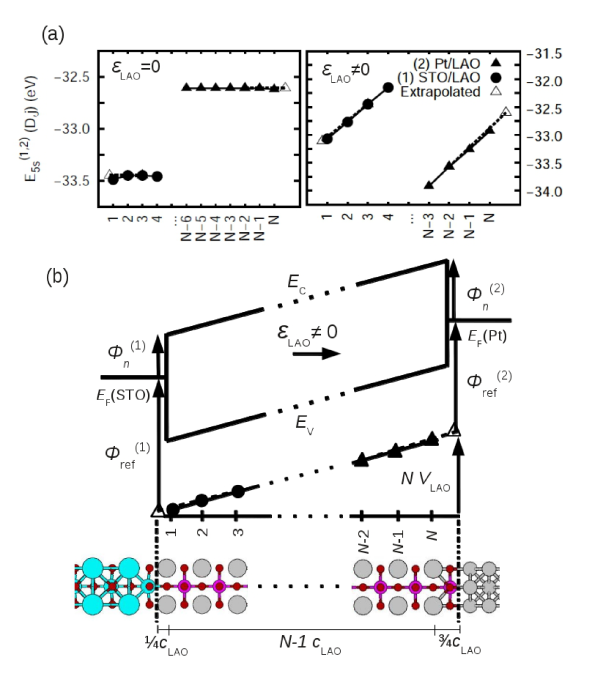
To extract the dependence of the SBH on , we use computational techniques similar to those in Refs. [stengel09b, ] and [stengel11b, ]. In particular, for the estimation of the band offset we need two independent quantities, the so-called lineup term (an interface property) and the band-structure term (a bulk property) stengel11b . The lineup term relies on the choice of a reference energy in the insulating LAO layer; here we use the La semicore energy, that we extract from the layer-resolved density of states of the slab models. We define as the energy location of the La peak in the -th LaO layer of the (1) or (2) system, referred to the respective Fermi level. In the case of zero field, converges to a constant value for layers lying sufficiently far away from the interface or the surface (typically two-three unit cells), and the definition of the lineup term is straightforward. Conversely, when the electric field in LAO is nonzero (see Fig. 2), has a linear dependence on the layer index. In particular, deep enough in the film, the variation of between two consecutive cells corresponds precisely to the bulk internal field at the same value of ,
| (2) |
Therefore, once is known (from the bulk calculations), we can define an extrapolated reference energy (see Fig. 2),
| (3) |
where the constant is chosen in such a way that far from the interface. Then, we define the lineup term as
| (4) |
where indicates the interface plane location; here we assume and (see Fig. 2). Finally, to obtain the -type SBH we just need to add to the -dependent band-structure term [we calculate it in the bulk, as the difference between the La level and the conduction band minimum], ,
| (5) |
Our results for and are shown in Fig. 3(a,b). We find that behave linearly within the whole studied range. Consequently, the total potential drop due to both interfaces can be expressed as , where is the total interface potential drop at and the coefficient physically corresponds to the overall inverse interface capacitance density stengel09 ; stengel09c . Considering the potential drop in bulk LAO also to be linear in [see Fig. 3(b)], i.e. , we obtain a simple yet very accurate analytical expression for the electric displacement field in LAO,
| (6) |
where m2/F, V, and m2/F (). The inverse bulk LAO capacitance density, , is directly related to the static dielectric constant of LAO, , via ; in our computational model we have . For a given value of , we compute the corresponding electric field using . [In the “exact” treatment we replace the average with the calculated , see the inset of Fig. 3(c)]. Our results for are shown in Fig. 3(c). It is worth noting that the outcomes of Eq. (1) [exact, considering non-linearities in ] and Eq. (6) (approximate) are in excellent agreement. In both cases we find that monotonically decreases with the inverse of LAO thickness, independently of the applied bias potential.
These results have important implications concerning the interpretation of the experiments reported in Ref. [singh11, ]. First, no intrinsic built-in LAO electric field exists in the short-circuited Pt/LAO/STO capacitor system, contrary to the assumptions of Singh-Bhalla et al. singh11 . Second, and most importantly, the uniform decrease of with LAO thickness in practice rules out the hypothesis of Zener tunneling that was used in Ref. singh11 to explain the abrupt increase of the tunneling current at . Indeed, as decreases with increasing , Zener tunneling becomes increasingly less likely in thicker films; note that in our model the LAO valence band never goes above the STO Fermi level unless a strong external potential eV is applied. An alternative interpretation of the aforementioned tunneling experiments rests on the results of Ref. cancellieri11 . Precisely at a thickness of unit cell, Cancellieri et al. reported the onset of in-plane strain relaxation in the LAO overlayer. Such relaxation processes are known to induce defects (e.g. cracks, or misfit dislocations) in the LAO film cancellieri11 ; wang08 . It is not unreasonable to think that these defects might constitute preferential paths for electron or hole conduction; also, these defect-mediated conduction processes might explain the hysteretic behavior of the electrical diagrams of Ref. singh11 . (The authors invoked the presence of switchable dipoles at the LAO/STO interface, which appears puzzling as neither LAO nor STO are ferroelectric.)
Finally, we shall comment on the microscopic mechanisms that lead to the calculated interface properties. The total interface capacitance density can be expressed as the sum of two contributions,
| (7) |
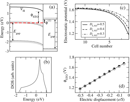
each due to a different interface. The variation of with is very small (see Fig. 3); this means that the Pt electrode behaves ideally (“perfect” screening stengel11b ), i.e. , and therefore we restrict the following analysis to the LAO/STO junction. Specifically, we shall consider the effects of band-bending on , i.e. the -dependent interfacial potential drop that occurs in STO due to the presence of the confined charge carriers yoshimatsu08 . To estimate the band-bending contribution, , we have employed the tight-binding (TB) model note2 introduced in Ref. stengel11 . We define as the value of the electrostatic potential in STO at the interfacial Ti site, referred to the Fermi level of the confined electron gas, at a given [see Fig. 4(a,c)]. Our results show that behaves linearly within a wide range of values [Fig. 4(d)]. The band-bending contribution to corresponds to the slope of the linear fit, which amounts to m2/F. This contribution constitutes a significant fraction (approximately two thirds) of . The remainder of is likely to be caused by other effects that typically occur at oxide-oxide interfaces, e.g. intrinsic dielectric “dead layers” nature2006 ; copie09 . As these appear to be of secondary importance here, we have not pursued this analysis further.
The above results are timely for the interpretation of recent capacitance measurements of thin-film electrode/LAO/STO heterostructures mannhart10 . In the regime of large carrier densities, Li et al. measured a dielectric constant of the LAO film of , which is significantly smaller than the typical value reported for LAO single crystals (). Our results indicate that this discrepancy may be related to interfacial effects, and in particular to the relatively small value of , rather than to the quality of the LAO film. It is worth noting that Li et al. mannhart10 used YBCO electrodes, instead of the Pt electrodes considered here. This implies that a possible contribution from the upper electrode interface should be in principle taken into account (recall that essentially vanishes in the present Pt/LAO case) when comparing our data to those of Ref. mannhart10 . In this context, note that Eq. (6) is completely general and applies to any electrode/LAO/STO configuration; one simply needs to replace two parameters (that are specific to the electrode/LAO interface), the Schottky barrier at zero field and the interface capacitance . In other words, one does not need to repeat the calculations of the LAO/STO interface, since we have essentially decoupled the bottom from the top electrode and their properties can be computed separately.
In summary, we have studied the electrical properties of metal/LAO/STO capacitors fully from first-principles, determining a complete physical picture of the band offsets and internal fields. Our results and methodologies open new avenues in the first-principles study of functional oxide heterostructures, and provide useful guidelines for the interpretation of the available experimental data on this system.
This work was supported by MICINN-Spain (Grants No. MAT2010-18113 and No. CSD2007-00041), ICREA, and the EC-FP7 project OxIDES (Grant No. CP-FP 228989-2). Computing time was kindly provided by BSC-RES and CESGA.
References
- (1) A. Ohtomo and H. Y. Wang, Nature (London) 427, 423 (2004).
- (2) S. Thiel et al., Science 313, 1942 (2006).
- (3) Cen et al., Nature Materials 7, 298 (2008).
- (4) W. M. Lü et al., Appl. Phys. Lett. 99, 172103 (2011).
- (5) R. Jany et al., Appl. Phys. Lett. 96, 183504 (2010).
- (6) G. Cheng et al., Nature Nanotechnology 6, 343 (2011).
- (7) G. Singh-Bhalla et al., Nature Physics 7, 80 (2011).
- (8) J. Mannhart and D. G. Schlom, Science 327, 1607 (2010).
- (9) R. Pentcheva and W. E. Pickett, Phys. Rev. Lett. 102, 107602 (2009).
- (10) K. Janicka et al., Phys. Rev. Lett. 102, 106803 (2009).
- (11) P. Delugas et al., Phys. Rev. Lett. 106, 166807 (2011).
- (12) Z. S. Popovic, S. Satpathy, and R. M. Martin, Phys. Rev. Lett. 101, 256801 (2008).
- (13) S. A. Chambers et al., Phys. Rev. Lett. 107, 206802 (2011); L. Qiao et al., Surface Science 605, 1381 (2011).
- (14) H. Chen, A. M. Kolpak, and S. Ismail-Beigi, Advanced Materials 22, 2881 (2010).
- (15) W-J. Son et al., Phys. Rev. B 79, 245411 (2009).
- (16) N. C. Bristowe, P. B. Littlewood, and E. Artacho, Phys. Rev. B 83, 205405 (2011).
- (17) M. Stengel, N. A. Spaldin, and D. Vanderbilt, Nature Physics 5, 304 (2009).
- (18) M. Stengel, Phys. Rev. Lett. 106, 136803 (2011).
- (19) X. Wu, M. Stengel, K. M. Rabe, and D. Vanderbilt, Phys. Rev. Lett. 101, 087601 (2008).
- (20) M. Stengel, D. Vanderbilt, and N. A. Spaldin, Nature Materials 8, 392 (2009).
- (21) P. E. Blöchl, Phys. Rev. B 50, 17953 (1994)
- (22) We used a plane-wave energy cutoff of Ry and a Monkhorst-Pack k-point grid for Brillouin zone sampling. In the geometry optimizations, atomic forces along the out-of-plane direction were imposed to be smaller than meV/Å .
- (23) The additional charge density is introduced by substituting a cation at the ferroelectric surface by a fictitious cation of different formal valence. As we are interested in exploring intermediate values of , we generated fictitious pseudopotentials that reproduced fractional nuclear charges.
- (24) M. Stengel et al., Phys. Rev. B 83, 235112 (2011).
- (25) M. Stengel, D. Vanderbilt, and N. A. Spaldin, Phys. Rev. B 80, 224110 (2009).
- (26) C. Cancellieri et al., Phys. Rev. Lett. 107, 056102 (2011).
- (27) Y. Wang, S. G. Kim, and I-W. Chen, Acta Materialia 56, 5312 (2008).
- (28) K. Yoshimatsu et al., Phys. Rev. Lett. 101, 026802 (2008).
- (29) This is based on an electronic -Hamiltonian describing the hoppings between Ti-centered orbitals, wherein the electrical boundary conditions are defined by the electric displacement field in LAO.
- (30) M. Stengel and N. A. Spaldin, Nature 443, 679(2006).
- (31) O. Copie et al., Phys. Rev. Lett. 102, 216804 (2009).