Electron temperature in electrically isolated Si double quantum dots
Abstract
Charge-based quantum computation can be attained through reliable control of single electrons in lead-less quantum systems. Single-charge transitions in electrically-isolated double quantum dots (DQD) realised in phosphorus-doped silicon can be detected via capacitively coupled single-electron tunnelling devices. By means of time-resolved measurements of the detector’s conductance, we investigate the dots’ occupancy statistics in temperature. We observe a significant reduction of the effective electron temperature in the DQD as compared to the temperature in the detector’s leads. This sets promises to make isolated DQDs suitable platforms for long-coherence quantum computation.
Quantum mechanical charge and spin states of electrons confined in semiconductor double quantum dots (DQD) hanson ; haya ; peter have recently attracted much interest, as they can be exploited to implement solid-state quantum computation. One key requirement to perform quantum logic operations is a long coherence time for the qubit-embodying states. Among other system materials, silicon is particularly suited to retain spin-coherence for long time mainly due to the existence of a stable isotope (28Si) without nuclear magnetic moment. tyry Another approach to mitigate the decoherence introduced by the interaction with the environment is the suppression of exchange processes with electrons in the reservoirs. yurke This has proven to be beneficial if a charge-qubit implementation is to be preferred. Indeed, single-qubit operations have been successfully implemented in trench-isolated silicon double quantum dots, gorman where electrons are confined in a lead-less system and only capacitively coupled to gates.
Here, we investigate the electronic occupation of phosphorus-doped isolated DQDs using a single-electron tunnelling device (SET) as a charge sensor. By means of time-resolved charge detection, the probability of occupation of each dot is evaluated as the control gate is swept across a degeneracy point (i.e. alignment of energy levels which leads to electron tunnelling). From these measurements we have extracted the electron temperature in the isolated quantum system and compared it with the one measured in the SET leads. The advantageous effects of a lead-decoupled system are quantitatively observed as a significant temperature reduction in the DQD.
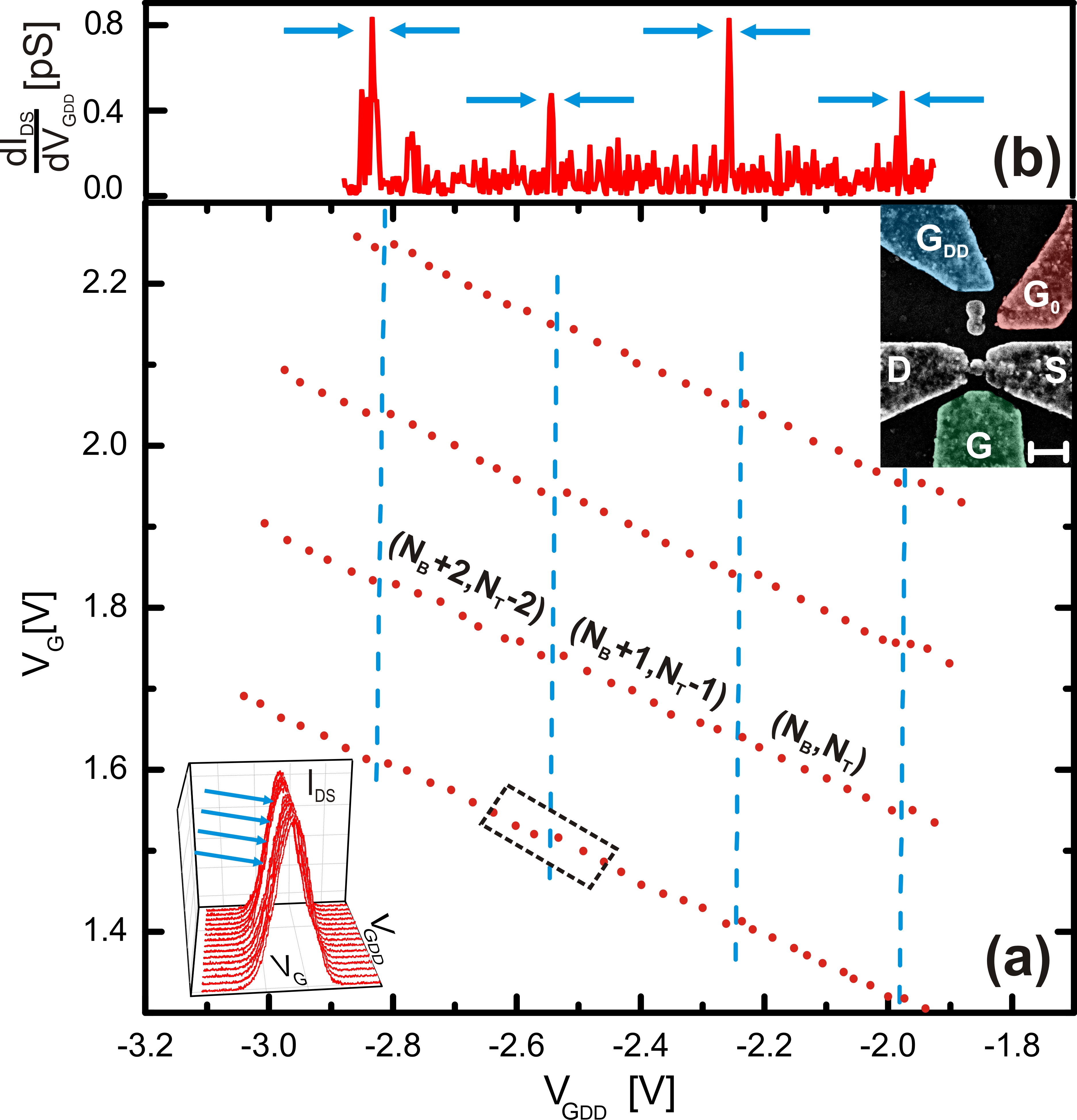
The top inset of Fig. 1(a) shows a scanning electron micrograph (SEM) image of a representative device. The use of silicon-on-insulator wafers ensures spatial confinement of electrons in the vertical direction; reactive ion etching is used to define deep trenches which produce confinement within the horizontal plane. The silicon active layer is doped with a concentration of phosphorus atoms of about 31019 cm-3 to provide the nano-structure with free carriers. From the density of implanted donors, we estimate that a 40 nm diameter dot contains about 2000 electrons. Both electron-beam and optical lithography are employed to define the device pattern. Full details of the fabrication process, tunnel barriers formation and influence of interface trapping for this system are reported elsewhere. myJAP In order to keep the operating point of the detector in the most sensitive region while inducing transitions in the DQD, gates G and GDD are simultaneously swept with a fixed ratio. By contrast, gate G0 is always kept at a fixed voltage. Experiments have been performed in a 3He cryostat at the base temperature 295 mK, unless otherwise stated.
Fig. 1(a) shows the positions of the detector’s Coulomb peak maxima as a function of the voltage applied to gates GDD and G. The plot reveals the occurrence of Coulomb Blockade (CB) in the SET; the resonances’ slope indicates that both gates are coupled to the SET island and significantly affect its potential. In particular, it is possible to determine the relative strength with which each gate is coupled to the SET in terms of gate capacitance ratio. Indeed, the slope of the CB features () directly reflects the ratio between the SET gate capacitances (see left inset of Fig. 3), which can be written as ; this defines the voltage compensation ratio needed to keep the SET at a fixed bias point. Most interestingly, we observe that the trajectory of the conductance peaks in [,] space is nearly periodically shifted. In the bottom inset, the shift highlighted by the dashed rectangle is shown as a misalignment between two adjacent groups of peaks in two-gate voltage space. As previously reported,myAPL this effect is the clear signature of single-charge tunnelling within the nearby DQD structure; in particular, for more negative we expect electrons to move from the top dot (T) to the bottom one (B). Each of these events produces a shift of about 1 of a CB period which is equivalent to an induced charge in the SET island of 0.01, where is the elementary charge. This directly depends on the amount of mismatch in the coupling of each dot to the detector, as it has been found myAPL that , where is the modification of the SET island potential upon a tunneling event in the DQD, () is the coupling capacitance between the top (bottom) dot and the SET island and () is the total self-capacitance of the top (bottom) dot. It is worth noting that the shifts have all nearly equal amplitude (1) and draw parallel lines (see dashed lines in the main plot) that divide the voltage space in regions of stable charge distribution within the DQD. This symmetry indicates that the transitions originate all from the same spatial location (the DQD) which has a fixed capacitive coupling to both the charge sensor and the gate electrodes. Fig. 1(b) depicts the differential conductance of the detector as the gate voltages and are mutually compensated along the trajectory followed by the lower CB resonance in (a) to keep maximum charge sensitivity. Sharp resonances clearly appear in correspondence of the voltage shifts; this reflects, once more, the occurrence of discrete changes in the electrostatic potential of the SET due to remote charge transfer.
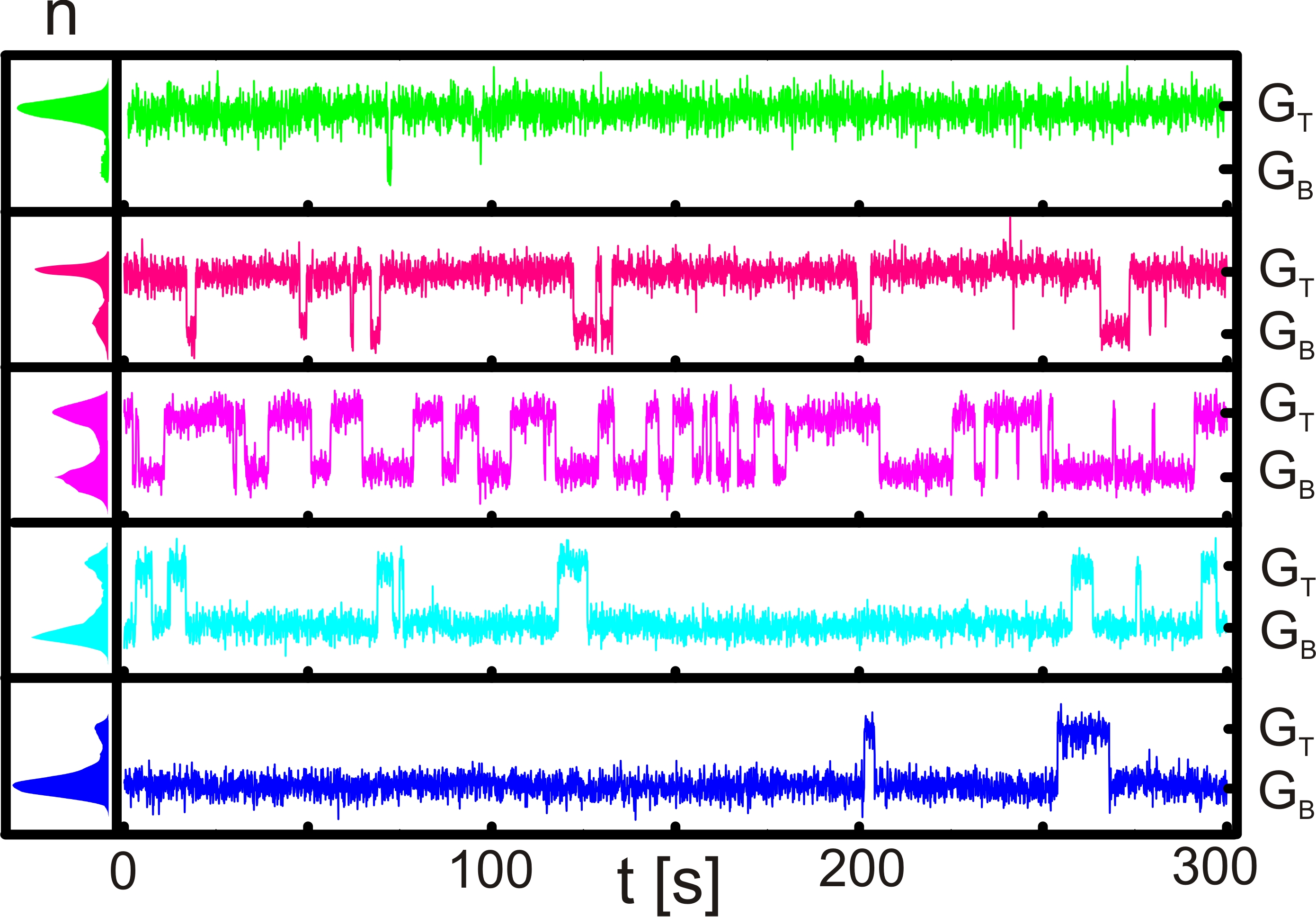
In order to observe the time-dependent evolution of the DQD near a transition, traces are recorded for different gate voltages across a degeneracy point. In Fig. 2 we report five representative traces of the SET conductance for time intervals of 300 s at a sampling frequency of 13 Hz. Data are taken in the vicinity of the transition shown in the inset of Fig. 1(a). It is evident that near the degeneracy point the system switches randomly between the two states associated with two discrete conductance levels of the SET (i.e. and for an electron occupying the top and the bottom dot, respectively). The fraction of time that the system spends in each state is a function of the gate voltage and approaches 50 at the degeneracy point (central trace). Such an information can be extracted from the time-dependent plots by counting the number of points, , per conductance bin. A histogram of versus conductance is reported next to each relevant trace. The histograms allow one to directly visualize how gate voltages control the crossover from localised to delocalised charge states.
The presence of a range of gate voltages for which the system is degenerate (as opposed to sharp transitions at a single-valued voltage) suggests that tunnelling is affected by inelastic scattering processes mainly due to electron-phonon interactions. The gate voltage spread across the transition can be used to extract information on the energy level broadening and the effective electron temperature in the isolated DQD structure. From histograms similar to those shown in Fig. 2, the distribution functions of Fig. 3(a) can be built by converting the gate voltage into energy scale,
| (1) |
where is the lever arm of gate GDD to the DQD, and are the degeneracy point electrochemical potential and voltage, respectively. Following the theory by Beenakker, beenak we can treat the discrete energy spectrum in the DQD as a continuum, given that for our system , being the Boltzmann’s constant, the electron temperature in the DQD, the single-particle level separation and the dots’ charging energy. Under this assumption, the distribution function can be approximated by the Fermi-Dirac (FD) distribution,
| (2) |
from which the effective electron temperature can be extracted. It is worth pointing out that our system largely satisfies the classical limit approximation as 17 meV, 30 eV and 20 eV. Fig. 3(a) depicts three representative distributions for different values of . Solid line fits allow one to estimate the values of which appear not to be affected by the base temperature up to approximately 500 mK, as shown in Fig. 3(b) (squared data points). Indeed, it is clear from the fitting lines in blue that for 500 mK, 500 mK whereas for 500 mK, . This is the evidence that the lowest limit for the electron temperature in the DQD is set to roughly 500 mK by our cryogenic set-up. In order to correctly extract the electron temperature from the occupancy distributions, it is paramount to know precisely the value of to be used in Eq. (1). Given that direct transport measurements are not allowed due to the isolated nature of the DQD, the estimate of has been attained as follows. Initially, we have used a value of first attempt by assuming 0.033 eV/V, where is the lever arm of gate G to the SET. This can be easily extracted from the diamond plot of the detector. Next, from the observation that is nearly constant up to 500 mK, we have fitted the occupancy distribution at 500 mK using as a fitting parameter and 500 mK as a fixed parameter. The final value of the lever arm so obtained is 0.055±0.001 eV/V. The fact that the line of best fit in Fig. 3(b) for 500 mK satisfies the condition is a decisive consistency check which corroborates the approach used to evaluate the lever arm.
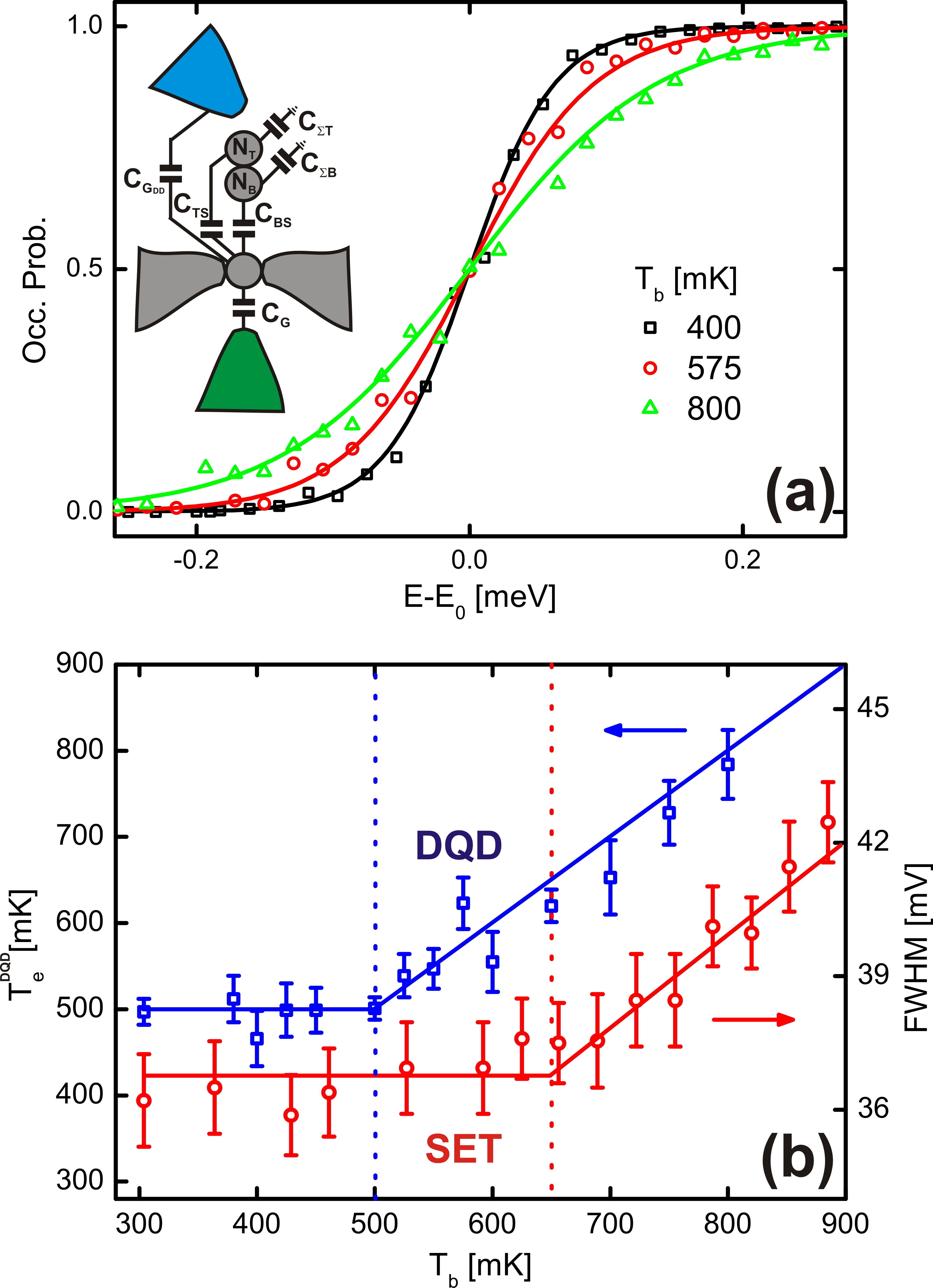
It is now interesting to compare the value of minimum electron temperature for the DQD and the detector’s leads. To this end, we measure the full width at half maximum (FWHM) of the Coulomb peaks in the SET as the base temperature of the cryostat is increased. We find that the width scales linearly with temperature foxman from a minimum value 650 mK, which is an estimate of the electron temperature in the detector (see dotted data points in Fig. 3(b)). The discrepancy between the two electron temperatures is a convicing manifestation of the beneficial effects of decoupling quantum systems from leads electrically connected to room temperature electronics. However, the presence of other concurrent heating mechanisms in the DQD is indicated by the fact that the lowest is larger than any base temperature value below 500 mK, which is unexpected for an isolated system in thermal equilibrium with the phonon bath. A number of reasons may be the cause of this effect. Firstly, the presence of the charge detector in the vicinity of the DQD may produce heating exchange due to phonon-mediated back-action. gas In other words, the current flowing through the SET produces ohmic dissipation in the leads that can be absorbed by the phonon bath and transferred to the electrons in the DQD. If this mechanism turned out to be dominant, we would observe modifications in the value of as a function of the detector’s bias point. This will be the focus of further investigations. Moreover, the weak coupling between the electrons and the phonon bath, which is typically in place in nano-scale systems because of finite-size effects, tilke ; ziman should be considered. This may lead to exceedingly long thermalisation times on the scale of the time-resolved experiments presented here and consequently result in an increase of the electron temperature. Finally, a temperature difference may also arise due to some difficulty in attaining premium thermal conduction between the condensed 3He and the cold finger where the device is plugged in.
In conclusion, this work has shown that control of charge state can be achieved in fully electrically isolated DQD systems. Most interestingly, we have demonstrated that the benefit of decoupling the DQD from the leads can be quantitatively estimated as a strong reduction in electron temperature. Given that the mitigation of decoherence sources is a crucial requisite for reliable quantum manipulations, this system promises to be a viable candidate for charge-based quantum computation.
This work was partly supported by Project for Developing Innovation Systems of the Ministry of Education, Culture, Sports, Science and Technology (MEXT), Japan.
References
- (1) R. Hanson, L. P. Kouwenhoven, J. R. Petta, S. Tarucha, and L. M. K. Vandersypen. Rev. Mod. Phys., 79:1217–1265, 2007.
- (2) T. Hayashi, T. Fujisawa, H. D. Cheong, Y. H. Jeong, and Y. Hirayama. Phys. Rev. Lett., 91:226804, 2003.
- (3) K. D. Petersson, J. R. Petta, H. Lu, and A. C. Gossard. Phys. Rev. Lett., 105:246804, 2010.
- (4) A.M. Tyryshkin, J.J.L. Morton, S.C. Benjamin, A. Ardavan, G.A.D. Briggs, J.W. Ager, and S.A. Lyon. J. Phys.: Condens. Matter, 18:S783, 2006.
- (5) I.V. Yurkevich, J. Baldwin, I.V. Lerner, and B.L. Altshuler. Phys. Rev. B, 81:121305, 2010.
- (6) J. Gorman, D. G. Hasko, and D. A. Williams. Phys. Rev. Lett., 95:090502, 2005.
- (7) A. Rossi and D.G. Hasko. J. Appl. Phys., 108:034509, 2010.
- (8) A. Rossi, T. Ferrus, G. J. Podd, and D. A. Williams. Appl. Phys. Lett., 97(22):223506, 2010.
- (9) C. W. J. Beenakker. Phys. Rev. B, 44:1646–1656, 1991.
- (10) E. B. Foxman, U. Meirav, P. L. McEuen, M. A. Kastner, O. Klein, P. A. Belk, D. M. Abusch, and S. J. Wind. Phys. Rev. B, 50:14193–14199, 1994.
- (11) U. Gasser, S. Gustavsson, B. Küng, K. Ensslin, T. Ihn, D. C. Driscoll, and A. C. Gossard. Phys. Rev. B, 79:035303, 2009.
- (12) A. Tilke, L. Pescini, A. Erbe, H. Lorenz, and R. Blick. Nanotech., 13:491, 2002.
- (13) J. Ziman. Electrons and phonons. Clarendon, Oxford, 1960. p.307.