Soft nanostructuring of YBCO Josephson Junctions by phase separation
Abstract
We have developed a new method to fabricate biepitaxial YBa2Cu3O7-δ (YBCO) Josephson junctions at the nanoscale, allowing junctions widths down to 100 nm and simultaneously avoiding the typical damage in grain boundary interfaces due to conventional patterning procedures. By using the competition between the superconducting YBCO and the insulating Y2BaCuO5 phases during film growth, we formed nanometer sized grain boundary junctions in the insulating Y2BaCuO5 matrix as confirmed by high resolution transmission electron microscopy. Electrical transport measurements give clear indications that we are close to probing the intrinsic properties of the grain boundaries.
Microtechnology and Nanoscience] Department of Microtechnology and Nanoscience, Chalmers University of Technology, SE-412 96 G teborg, Sweden Microscopy and Microanalysis]Microscopy and Microanalysis, Department of Applied Physics, Chalmers University of Technology, SE-412 96 G teborg, Sweden Microtechnology and Nanoscience] Department of Microtechnology and Nanoscience, Chalmers University of Technology, SE-412 96 G teborg, Sweden Microscopy and Microanalysis]Microscopy and Microanalysis, Department of Applied Physics, Chalmers University of Technology, SE-412 96 G teborg, Sweden Microtechnology and Nanoscience] Department of Microtechnology and Nanoscience, Chalmers University of Technology, SE-412 96 G teborg, Sweden Microtechnology and Nanoscience] Department of Microtechnology and Nanoscience, Chalmers University of Technology, SE-412 96 G teborg, Sweden
This document is the Accepted Manuscript version of a
Published Work that appeared in final form in Nano Letters,
copyright ©American Chemical Society after peer review and
technical editing by the publisher. To access the final edited and
published work see
http://pubs.acs.org/doi/full/10.1021/nl103311a
With the advances in nanotechnologies it has become important to
develop quantum limited sensors which allow to measure the physics
of very small objects with nanometer size resolution. Josephson
junction based nanodevices, as an example nanoSQUIDs
(Superconducting Quantum Interference Device), are very attractive
for their extreme sensitivity to magnetic flux which should allow as
ultimate goal the detection of individual spin1, for their
potentiality in quantum informatics processing based on spin
systems2 and for their employment in scanning SQUID
microscopy3. The miniaturization of the Josephson
junctions is the key issue in this area. Recent advances have
prioritized simple fabrication procedures which have led to the use
of nanobridge junctions instead of the commonly used Josephson
tunnel junctions. In this way planar Al and Nb nanoSQUIDs with
excellent noise performances have been fabricated with a single
layer superconductive film by e-beam lithography1 or
Focused Ion beam (FIB)4. The assessment of single
layer technology for nanoscale high-temperature superconductor (HTS)
Josephson junctions would certainly push this field forward. HTS
nanoSQUIDs would allow to study magnetic nanoparticles at much
higher magnetic fields when compared to low critical temperature
superconductors (LTS).
The miniaturization of HTS oxides has followed different nanofabrication routes compared to the LTS counterpart. There are two main reasons: a) The high temperature involved in the epitaxial growth of thin films ( 700∘C) makes standard lift- off patterning procedures not applicable and b) conventional Reactive Ion Etching (RIE) techniques have proven to be ineffective. At present HTS nanostructures are realized by e-beam lithography in combination with a hard mask5 and ion milling etching or by focus ion beam patterning.67 In both cases the lateral damage of the structures is quite severe due to structural and chemical changes mostly related to oxygen out diffusion and/or Ga implantation. This fact puts severe limits to the smallest HTS Josephson tunnel junction size that can still retain its superconducting properties. In as-fabricated 200 nm wide tunnel junctions the superconductive properties are lost during the fabrication process and only partially recovered after post annealing treatment8. Some progress has recently been achieved in fabricating HTS nanoSQUIDs employing nanobridges9. However because of the extremely short coherence lengths of HTS superconductors ( of the order of 1-2 nm in the a-b planes for YBCO) the Josephson -like effect in HTS nanobridges is still not well understood. The nanoSQUIDs have a narrow range of working temperature, close to the critical temperature of the nanostructure, which removes one of the main advantage in using HTS based nanosensors.
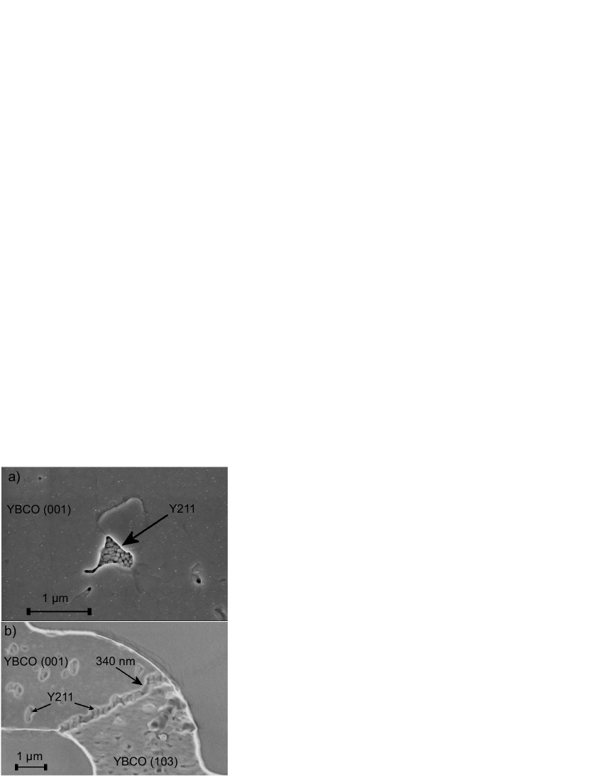
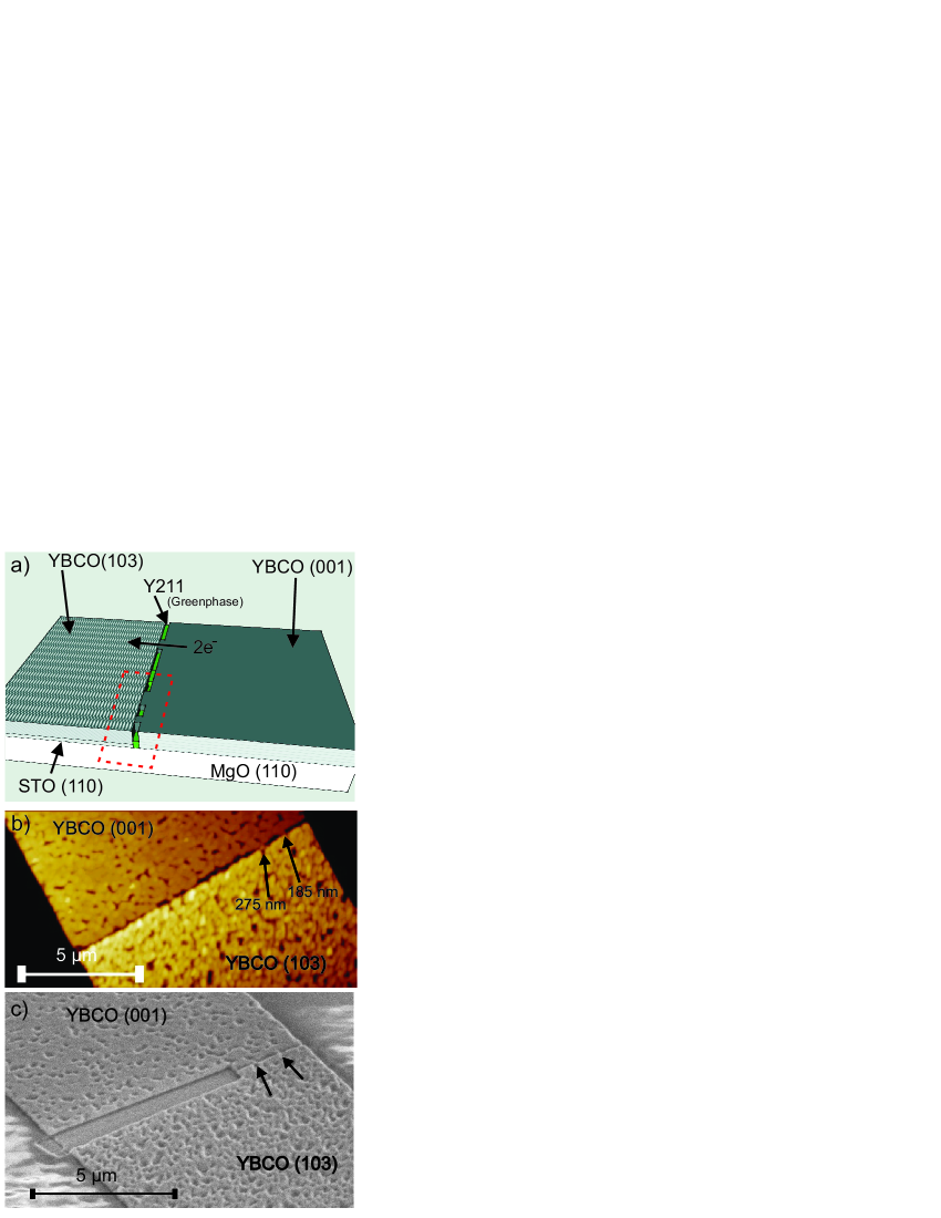
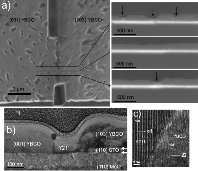
In this letter we present a new method which combines conventional nanofabrication techniques with self assembly concepts to fabricate Josephson tunnel junctions at the nanoscale. The junctions are realized by the biepitaxial grain boundary technique which is based on a single layer HTS film. The main idea relies on the competition between superconductive and insulating phases during thin film growth. On specific substrates like MgO (110) the superconductive YBa2Cu3O7-δ (Y123) with [001] orientation competes with the Y2BaCuO5 (Y211) insulating phase,1011 often referred to as green phase. In figure 1 a) a SEM picture shows the two different growths. Previous studies, made on sputtered thin films, have shown that non optimal deposition conditions and the presence of grain boundaries10 strongly enhance the nucleation of the green phase. By realizing grain boundary junctions on MgO (110), one can expect to reach specific growth conditions where nanometer size YBCO grain boundaries will be naturally embedded in a green phase matrix (see figure 2 a)).
In what follow we will give a proof of principle of our novel soft nanopatterning by presenting the transport properties of nanojunctions and nanoSQUIDs. The validity of our approach has been further confirmed by transmission electron microscopy (TEM). The TEM provides information about the subsurface structure of the film and also about the interface between the film and the substrate. TEM studies are quite crucial since the superconducting thin film used in this work are deposited by laser ablation and not by sputtering as in previous works10. The different kinetics of growth of the two deposition techniques could strongly affect the nucleation of the greenphase and its competition with the superconductive Y123. The transport properties of nanoscale Josephson junctions fabricated by the soft nanopatterning technique have also been compared with those of junctions obtained by conventional nanofabrication procedures using an amorphous carbon mask defined by e-beam lithography and ion milling (see Stornaiuolo12 et al. for details on the fabrication process).
Biepitaxial grain boundary junctions are fabricated on MgO (110) substrates using a 20 nm thick STO (110) film as seed layer. The STO is deposited by laser ablation at an oxygen pressure of 0.2 mbar and a deposition temperature of 680∘C. The STO film is partially removed from the substrates by first defining an amorphous carbon mask using e-beam lithography and finally etching the unwanted part in an ion beam milling system13. A 100-120 nm thick YBCO film is then deposited by laser ablation at an oxygen pressure of 0.6 mbar using a deposition temperature of 790∘C for the conventional method and a non optimal 740∘C for the soft pattering technique to enhance the greenphase growth. The Y123 film grows [001] oriented on the MgO and [103] on the STO. In the films grown at lower deposition temperature the Y123 is the dominating phase but Y211 appears randomly on the MgO side while strongly increasing at the MgO/STO step, see figure 1 b). The fabrication of soft patterned nanometer size junctions can be divided into two main steps:
-
1.
10 m wide grain boundary junctions are patterned using e-beam lithography and ion etching. The grain boundary interfaces are then imaged using Atomic Force Microscopy (AFM) and Scanning Electron Microscopy (SEM) to locate single or closely spaced double nano-connections (see figure 2 a)).
-
2.
Nanojunctions and nanoSQUIDs are then formed by isolating the Y123 nano connection(s) by FIB. Since the nano devices are embedded in a green phase matrix, their lateral sides will not be touched by the etching procedure. Typically the distance between the nano junction and the ion beam is at least 300-400 nm leaving the nano junction unharmed.
Figure 2b) shows an AFM image of a grain boundary interface before, and figure 2c shows a SEM image after the FIB cut. In the final structure two junctions, 275 nm and 185 nm wide respectively, have been preserved to form a nanoSQUID with a loop area of the order of 0.1 m2.
Electrical measurements were performed both when the interfaces were still 10 m wide, and after the FIB procedure used to isolate nanojunctions or nanoSQUIDs. The 10 m wide junctions were also measured before and after acquiring an image using an Ion Ga-source with the same energy as the one used to fabricate the nanodevices. Since the current-voltage characteristic (IVC) only changed a few percent we concluded that the properties of the nanojunctions forming the parallel array were not affected by the FIB cutting procedure.
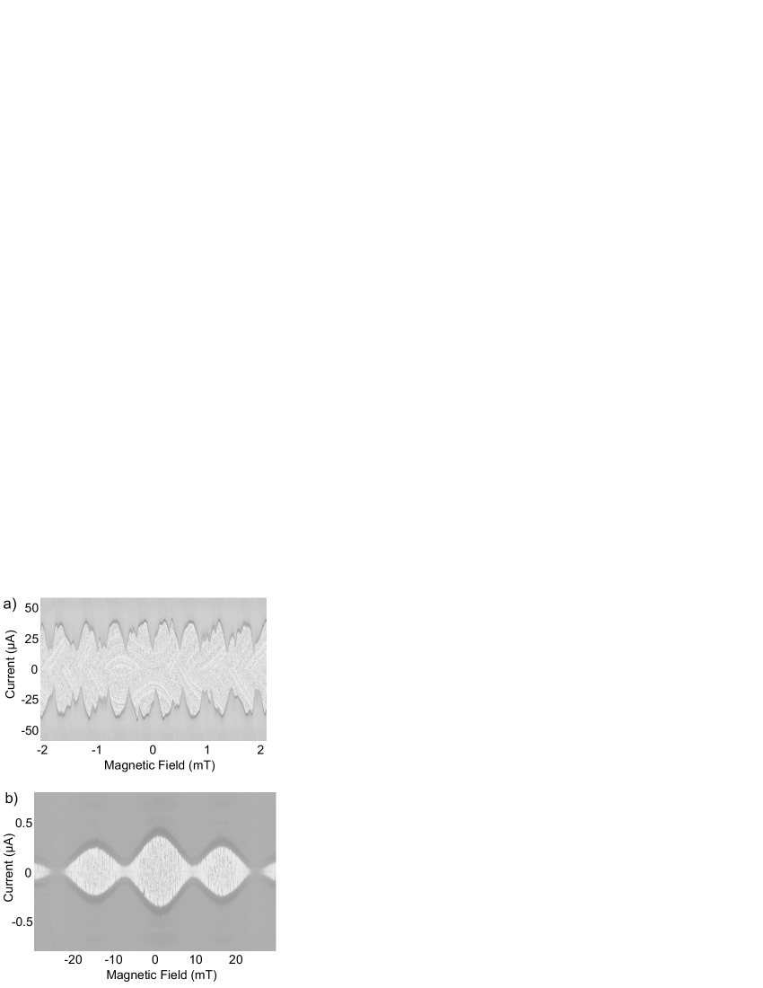
For all samples we have recorded the critical current (IC) dependence on the external magnetic field (B). This measurement is an important tool to get information about the uniformity of the critical current distribution across the grain boundary. All the electrical measurements were carried out at 280 mK and 34 K using an Oxford Instruments Heliox VL 3He system. We have characterized a number of single nanojunctions and nanoSQUIDs. Figure 3 a) shows the modulation pattern for the 10 m wide interface before the FIB cut and figure 3 b) after a single nanojunction is isolated by the FIB procedure. The behavior of the vs B pattern before the cut shows quick and irregular modulation and resembles that of an array of parallel connections14. After the cut, the magnetic pattern follows an almost ideal Fraunhofer like behavior as expected for a single Josephson junction15. From the period of the magnetic modulation (B) of the Josephson current one can extract a value for the junction width and compare it with that estimated by AFM/SEM pictures. Following Rosenthal and coworkers16 the expression for B which includes demagnetization effects is17 B=t/[. Here is the magnetic flux quantum, is the London penetration depth, t is the thickness of the film, d and w are the length and width of the junction respectively. We have applied this formula to a number of single junctions and the values were in good agreement with the ones extracted from AFM/SEM pictures differing at most by a factor less than 40%. From the magnetic pattern of figure 3b we got w 100 nm which explains why this nanojunction was not distinctively seen in the AFM picture.
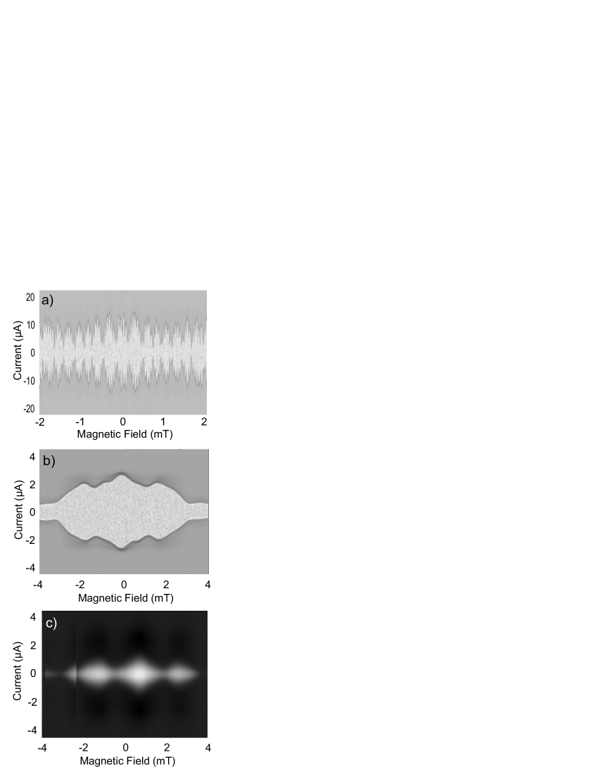
Figures 4 a) and b) show the IC vs B measurements for a nanoSQUID, before and after the cut respectively. When the structure is cut down to leave two connections separated by an area of insulating Y211, the IC vs B clearly shows a SQUID like pattern. Two different modulations are distinguishable; a faster one, due to the magnetic flux linked to the SQUID loop and a slower modulation originating from the IC vs B of two junctions. Because of the extremely small SQUID loop area (less than 0.1 m2) even though the junctions’ widths are on the nanoscale they cannot be considered point-like. In this case the slower modulation has a Fraunhofer like pattern that acts as an envelope over the faster SQUID modulation18. A hump can be noticed on the side of the inner lobes. This can be accounted for by considering that the current-phase relation (CPR) of Josephson junctions with a d-wave order parameter is unconventional and will have a significant second harmonic component.1920 Figure 4 c) shows the IC vs B dependence of the same nanoSQUID at 34 K. The increase in the modulation depth with temperature can probably be attributed to a different temperature dependence of the two components (first and second harmonics) in the current phase relation.1920 Flux trapping at the greenphase spots, in the wide electrodes, makes magnetic field measurements at temperatures higher than 40 K quite challenging. This can be improved by optimizing the geometry of the electrodes.2122 However since the Josephson current has an almost linear temperature dependence we expect working nanoSQUIDs at temperatures close to 77 K.
The dramatic change in magnetic field dependence of the Josephson current after the FIB procedure gives strong indications that our new soft nanostructuring approach works. However, It do not allow to distinguish, in an unambiguous way, between a grain boundary consisting of an array of parallel nanochannels and a single grain junction with a highly nonuniform critical current distribution. This would be a possible scenario, for example, if the nucleation of greenphase is not on the bare MgO(110) substrate but on a thin superconductive layer due to overgrowth. To confirm that we are probing an array of YBCO nanochannels embedded in a insulating greenphase matrix it is important to show that the greenphase particles extends all the way from the substrate/film interface up to the film surface. This information cannot be extracted using SEM. We have used high resolution TEM to reveal the interfacial microstructure with high spatial resolution in combination with electron diffraction to confirm the crystal structure of Y2BaCuO5. The TEM specimen were prepared using a combined FIB/SEM that allowed site specific extraction of grain boundary junctions. Here we show the results for a nanoSQUID with approximately the same dimensions as that of figure 4 showing the same Josephson phenomenology. Cross section SEM images were recorded during the specimen preparation, see figure 5 a). A greenphase particle adjacent to a YBCO nanochannel is seen in figure 5 b). It should be noted that the particle had nucleated at the film/substrate interface and extended all the way up to the film surface. Electron diffraction and Fourier transforms of high resolution TEM images showed that the particle was of the Y2BaCuO5 phase. This was in accordance with the energy dispersive x-ray (EDX) analysis.
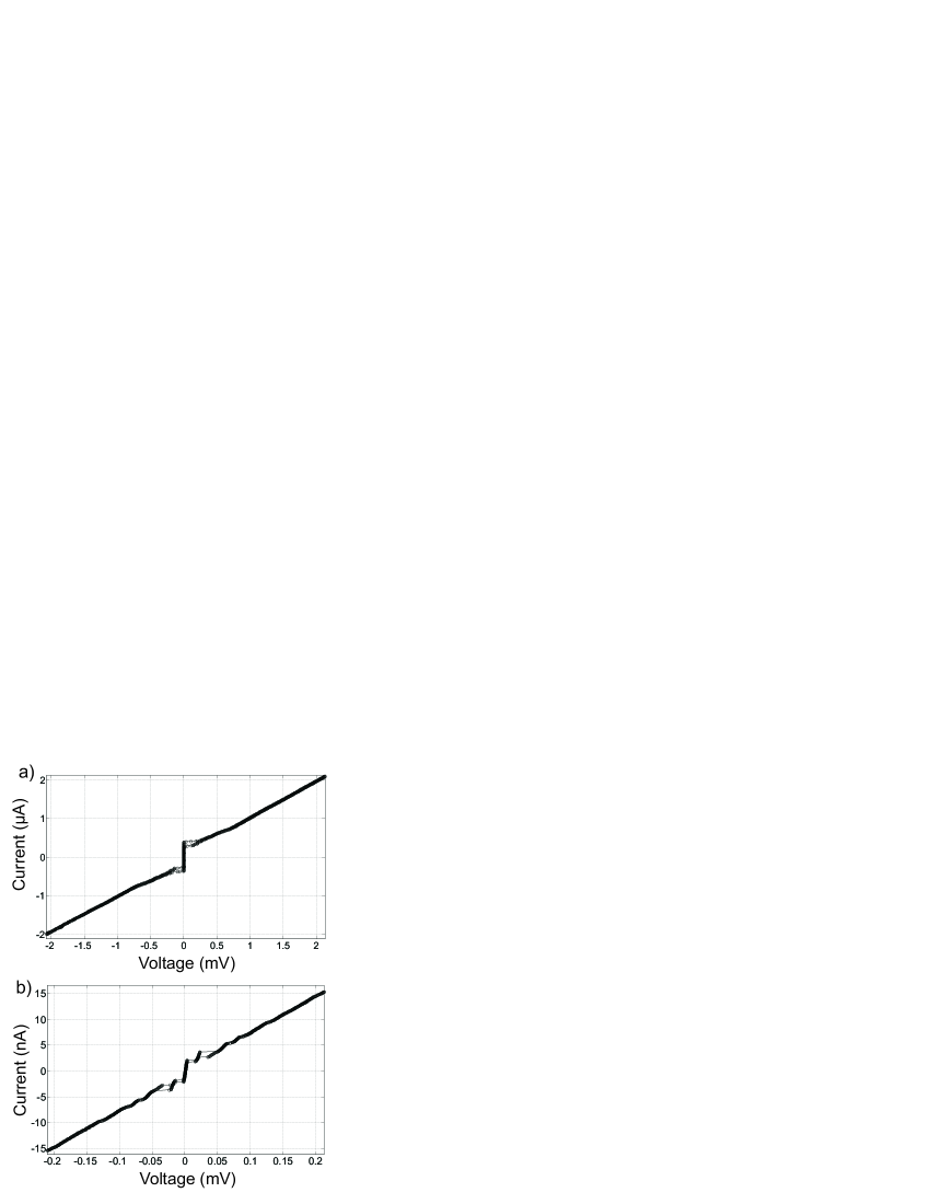
It is now important to compare the transport properties of nanoscale biepitaxial Josephson junctions made by soft nanopatterning with those fabricated with conventional methods. Figure 6 a) shows the current voltage characteristic (IVC) of a nanojunction made by soft nanopatterning. The curve follows the Resistively Capacitively Shunted Junction (RSCJ) model. A small hysteresis is visible and it is typical for most of the nanodevices. Because of the extremely small dimensions of the Josephson devices, we cannot rule out that the hysteresis is due to heating23. For comparison figure 6 b) shows the IVC of a sample of similar dimensions fabricated by conventional nanopatterning. The two curves show a clear difference in order of magnitudes both in Josephson current and normal resistance.
A more detailed examination of the current voltage characteristics for conventional junctions having widths in the range 200-300 nm gives a clear understanding of the extent of the lateral damage. For junctions fabricated using the conventional method with nominal width of 200 nm no Josephson effect was observed, they instead showed a highly resistive IVC (R 100 k - 100 M). Only junctions with widths of at least 300 nm had a finite critical current.
From the modulation period of the (B) patterns for the junctions fabricated using the conventional method it is possible to get an estimation for the effective width of the superconducting region and in this way determine the extent of the lateral damage. Considering the expression:1624 B=1.84 one can retrieve the actual width of the superconducting junction, weff. The conventionally fabricated junction shown in figure 6 b) modulates on a field scale on the order of Tesla. For these field scales flux trapping is an issue. The recorded magnetic pattern was quite irregular with several jumps in . However, we were able to unambiguously extract a modulation period of 1 T which gives weff60 nm. The nominal size of this junction is 300 nm which indicates that a significant part of the grain boundary has lost its superconductive properties during the milling process. This estimation together with the fact that all 200 nm wide junctions do not show any Josephson effect, is consistent with a non superconducting layer of more than 100 nm formed on each side of the device, also inferred by other groups8. This effect clearly limits the smallest size we can achieve with the conventional method.
On average samples fabricated with the soft patterning method have critical current densities (JC) in the range 103-104 A/cm2. Using conventional fabrication techniques we get junctions which have JC in the range 100 - 103 A/cm2. Typical values for the specific interface resistivites, =RNA, are in the range 10-8 - 10-7 cm2 for soft nanopatterning and 10-7-10-2 cm2 for conventional nanofabrication. Here RN is the normal resistance of the nanojunction extracted from the IVC and A is the junction area.
The huge spread in JC and for junctions fabricated with conventional nanopatterning is certainly related to the randomness in dimension of the superconductive grain boundary which survives the ion milling process. However this effect alone cannot account for the order of magnitude lower JC and higher of the conventional nanojunctions compared to those fabricated with soft nanopatterning. Instead, it clearly indicates that the conventional technique creates grain boundaries that are damaged and underdoped. These facts allow us to conclude that by the soft patterning technique we can, for the first time, get access to pristine grain boundaries which opens new prospectives to design experiments to study the intrinsic properties of HTS at the nanoscale.
In conclusion we have developed a new nano fabrication process to obtain biepitaxial YBCO grain boundary Josephson junctions at the nanoscale. The main advantage of this technique compared to conventional nanofabrication methods is that the grain boundaries are unharmed by the nano patterning. Electrical transport measurements in an externally applied magnetic field of Josephson junctions and SQUIDs reveal very clean and homogeneous grain boundary interfaces. Such clean interfaces are crucial for fundamental studies of superconductivity in cuprate-materials. Moreover the accomplishment of nano junctions allow for the realization of nanoSQUIDs for single spin detection and quantum circuits implementing HTS grain boundary josephson junctions.
.
This work has been partially supported by EU STREP project MIDAS, the Swedish Research Council (VR) under the Linnaeus Center on Engineered Quantum Systems, the Swedish Research Council (VR) under the project Fundamental properties of HTS studied by the quantum dynamics of two level systems, the Knut and Alice Wallenberg Foundation.
References
- 1 Lam, S.K.H.; Tilbrook, D.L. Appl. Phys. Lett. 2003, 82, 1078-1080
- 2 Meier, F.; Levy, J.; Loss, D. Phys. Rev. Lett. 2003, 90, 047901
- 3 Foley, C.P.; Hilgenkamp, H. Supercond. Sci. Technol. 2009, 22, 064001
- 4 Troeman, A.G.P.; et al. Nano Lett. 2007, 7, 2152-2156
- 5 Komissinski, P.V.; H gberg, B.; Tzalenchuk, A.Y.; Ivanov, Z. Appl. Phys. Lett. 2002, 80, 1022-1024
- 6 Testa, G.; et al. Appl. Phys. Lett. 2004, 85, 1202-1204
- 7 Nagel, J.; et al. arXiv:1009.2657v1.
- 8 Herbstritt, F.; Kemen, T.; Marx, A.; Gross, R. J. Appl. Phys. 2002, 91, 5411-5418
- 9 Wu, C.H.; et al. Nanotechnology 2008, 19, 315304
- 10 Scotti di Uccio, U.; et al. Physica C 1999, 321, 162-176
- 11 Di Chiara, A.; et al. Physica C 1996, 273, 30-40
- 12 Stornaiuolo, D.; Rotoli, G.; Cedergren, K.; Born, D.; Bauch, T.; Lombardi, F.; Tafuri, F. J. Appl. Phys. 2010, 107, 113901
- 13 Miletto Granozio, F.; et al. Phys. Rev. B 2003, 67, 184506
- 14 Licharev, K. Dynamics of Josephson junctions and circuits, 1st edition
- 15 Tinkham, M. Introduction to Superconductivity, 2nd edition, Dover Publications, New York, 2004
- 16 Rosenthal, P. A.; Beasley,M. R.; Char,K.; Colclough, M.S.; Zaharchuk,G. Appl. Phys. Lett. 1991, 59, 2482-3483
- 17 for a Tc of 89 K is approximately 160 nm26. = 920 nm was obtained using = 2 m25 and geometrical considerations27 for a grain boundary angle of 40∘
- 18 Barone, A. Physics and Applications of the Josephson Effect, John Wiley Sons, New York, 1982
- 19 Lindstr m, T.; et al. Phys. Rev. B 2006, 74, 014503
- 20 L fwander, T.; Shumeiko, V.S.; Wendin, G. Supercond. Sci. Technol. 2001, 14, R53
- 21 Castellanos, A.; W rdenweber, R.; Ockenfuss, G.; Hart, A.v.d.; Keck, K. Appl. Phys. Lett. 1997, 71, 962-964
- 22 Dantsker, E.; Tanaka, S.; Clarke, J. Appl. Phys. Lett. 1997, 70, 2037-2039
- 23 Ransley, J.H.T.; et al. Phys. Rev. B 2004, 70, 104502
- 24 Due to the different geometry of the electrodes used for the junctions fabricated with conventional nanofabrication techniques, we need to use a different expresion for the modulation period valid when .
- 25 Homes, C. C.; et al. Phys. Rev. B 2005, 71, 184515
- 26 Zuev, Y.; Kim, M.S.; Lemberger, T. R. Phys. Rev. Lett 2005, 95, 137002
- 27 Johansson, J.; Cedergren, K.; Bauch, T.; Lombardi, F. Phys. Rev. B 2009, 79, 214513