Impact of electron heating on the equilibration between quantum Hall edge channels
Abstract
When two separately contacted quantum Hall (QH) edge channels are brought into interaction, they can equilibrate their imbalance via scattering processes. In the present work we use a tunable QH circuit to implement a junction between co-propagating edge channels whose length can be controlled with continuity. Such a variable device allows us to investigate how current-voltage characteristics evolve when the junction length is changed. Recent experiments with fixed geometry reported a significant reduction of the threshold voltage for the onset of photon emission, whose origin is still under debate. Our spatially resolved measurements reveal that this threshold shift depends on the junction length. We discuss this unexpected result on the basis of a model which demonstrates that a heating of electrons is the dominant process responsible for the observed reduction of the threshold voltage.
pacs:
73.43.-f, 72.10.FkI Introduction
The renewed interest in integer quantum Hall (QH) systems is principally motivated by the peculiar features of edge states.Halperin1982 They give rise to chiral one-dimensional channels that behave as perfectly collimated beams of electrons, whose trajectory,Paradiso2010 phase,Camino2005 ; Ji2003 ; Neder2006 ; Neder2007 ; Roulleau2007 back-scattering probability,Roddaro2003 ; Roddaro2004 ; Roddaro2005 ; Roddaro2009 and energy distributionAltimiras2010 can be accurately controlled. QH circuits are used as flexible building blocks for coherent transport devices, e.g. the electron analogue of the Fabry-Pérot,Camino2005 Mach-ZehnderJi2003 ; Neder2006 ; Neder2007 ; Roulleau2007 or Hanbury-Brown-TwissNederNature2007 interferometer. In recent years a number of experimentsWurtz2002 ; Nakajima2010 ; Paradiso2011 focused on a particularly promising scheme: two co-propagating edge channels are imbalanced by means of selector gates,Komiyama1989 ; Komiyama1992 then brought into close proximity along a path of finite length, and are finally separated. The junction so defined allows co-propagating edges to exchange either energy and/or charge. In particular the inter-channel charge transfer allows equilibrating the initial electro-chemical potential imbalance. The amount of scattered charge depends on the sample characteristics, on the length of the interaction path, and on the inter-channel bias.Paradiso2011 For small bias, the relevant equilibration process is elastic scattering induced by impuritiesKomiyama1989 ; Komiyama1992 that provide the required momentum difference between initial and final edge states. This hypothesis has been confirmed by spatially resolved measurementsParadiso2011 that related the local backscattering map to the specific impurity distribution.
For large bias, when the inter-channel imbalance exceeds the energy difference between Landau levels, also radiative transitions are observed.Ikushima2007 This effect has been recently exploited to implement an innovative converter from phase-coherent electronic states to photons in the THz region.Ikushima2010 While the occurrence of this radiative emission is well established, the interpretation of the threshold value is actually not clear. In fact, several papers showedKomiyama1989 ; Komiyama1992 ; Machida1996 ; Wurtz2002 ; Ikushima2010 that the threshold voltage is considerably smaller than the nominal Landau level gap . Some gap reduction mechanisms have been suggested,Wurtz2002 but spectroscopic studies evidenced no deviation of the photon energy from .Komiyama2006 Thus a convincing explanation for such a shift is missing so far.
In the present work we investigate how a finite imbalance is equilibrated along the junction length , by studying how current-voltage characteristics change when is varied. To this end, we exploited the scanning gate microscopy technique described in Ref. Paradiso2011, . The spectral analysis reported in section II reveals that the threshold voltage is lowered when the junction length increases and, at the same time, the transition in smoothened. In section III we analyze the relevant inter-channel scattering processes and develop a simple model which accounts for electron heating due to hot carrier injection. The electron temperature increase produces a reduction of the threshold value due to thermal broadening of the Fermi distribution. Finally, in section IV we quantitatively discuss the experimental data on the basis of this model and extract the electron temperature profile along the junction.
II Experimental results
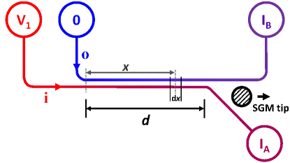
The experimental setup is described in detail in Ref. Paradiso2011, . Devices were realized starting from a high-mobility AlGaAs/GaAs heterostructure. The 2DEG is confined 55 nm under the sample surface. By Shubnikov -de Haas measurements we determined both the electron sheet density ( m-2) and mobility ( mV s). A 1D channel (6 m-long, 1 m-wide) was defined by two Schottky gates patterned on the sample. Measurements were performed at a base temperature of about 300 mK (electron temperature of about 400 mK) and bulk 2DES filling factor at T, which corresponds to a cyclotron gap meV. Figure 1 schematically illustrates our experiment: two cyclotron-split edge channels originate from two distinct voltage contacts at potential and , respectively. The channels meet at the entrance of a 1D channel and travel in close proximity for a distance before they are separated by the action of the electrostatic potential induced by the biased tip of a scanning gate microscope (SGM), as shown in detail in Ref. Paradiso2011, . We label the two channels as inner () and outer () channel with chemical potential and , respectively. After being separated by the SGM tip, the outgoing channels are guided to two detector contacts and .
For any value of the interaction distance compatible with device dimensions, i.e. from 0 to 6 m, we can measure the current-voltage (-) characteristics of the inter-channel charge transfer. Experimental data are shown in Fig. 2. The first relevant feature concerns the zero-bias differential conductance which monotonically increases with the interaction length . This is consistent with the differential conductance SGM plots reported in Ref. Paradiso2011, . The curves are asymmetric around zero. While the scattered current displays a non-linear but featureless dependence on for positive bias,note we will focus on the analysis of the negative bias range (, i.e. ), where a clear transition between two distinct linear regimes occurs. Two linear curve sections with different slope are separated by a kink, which occurs at a certain threshold voltage . We evaluate for each individual curve by extrapolating straight lines for both the small bias and the saturation regime and taking the abscissa of the intersection point, as explicitly shown in Fig. 2 for the m curve. For bias smaller than , the current-voltage characteristics are linear. The junction resistance between the two channels increases when is lowered. On the other hand, for the differential conductance saturates to , i.e. half of the total conductance, so that an increase of the input bias produces a voltage increase in both output edges. In fact the resulting output current is , and therefore . Thus, beyond the threshold, any excess of imbalance between the two edges is perfectly equilibrated.
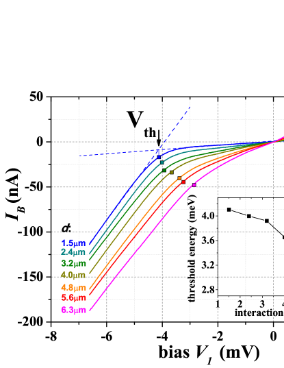
The most interesting feature in Fig. 2 concerns the detail of the transition between the two regimes, whose position and shape clearly depends on the interaction path length . The dependence of the actual threshold voltage on the junction length is shown in the inset of Fig. 2. It is always smaller than and is consistently reduced by increasing . At the same time the transition becomes smoother, as shown in Fig. 2. This is the main experimental finding of the present paper. It crucially depends on the opportunity, given by the SGM technique, to tune the junction length, keeping all the other parameters constant.
III Model for the inter-channel scattering
To discuss our model we will refer to the scheme shown in Fig. 1. The two edge channels meet at with an imbalance . Along the junction length the imbalance will decrease due to scattering events. In the model we assume an immediate intra-edge relaxation, so that both the chemical potential and the electron temperature are well defined for each position . In general, in each junction interval the scattered current is given by
| (1) |
where is a general function of and depending on the details of the equilibration model (edge dispersion, scattering mechanisms, electron heating etc.). The corresponding changes in the edge potentials are
| (2) |
where the factor 2 accounts for the spin degeneracy. From equations 1 and 2 we obtain:
| (3) |
The output edge currents are
| (4) |
whose sum equals the total input current .
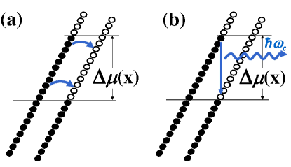
Inter-channel scattering can originate from several processes. For low bias, the inter-edge electron transfer can be either induced by impurity or phonon scattering.Komiyama1989 ; Komiyama1992 The latter, however, was shownKomiyama1989 ; Komiyama1992 to be less important when the base temperature is smaller than 1 K. The relevant process (sketched in Fig. 3(a)) is thus the elastic scattering induced by sharp impurity potentials which provide the change in momentum needed for the inter-channel transition. The infinitesimal scattered current in the interval is
| (5) |
where is the density of states around the energy and is the elastic scattering probability per unit time.
In order to estimate expressions as the one on the right hand side of Eq. 5, a model for the edge dispersion is needed. In this paper we will assume the simplest case, i.e. a linear dispersion, a choice that will be justified in Section IV on the basis of the observed temperature effects. In this approximation, we can assume both and as constant in the energy window . In this case the density of states is , where is the drift velocity. Thus (see appendix A)
| (6) | |||||
where is the constant transmission probability. For this process is linear in and does not depend on . - curves can thus be calculated by solving the ordinary differential equation 3 for with boundary condition , which gives an exponential decay of the edge imbalance
| (7) |
This exponential behavior was assumed in literatureKomiyama1989 ; Komiyama1992 ; Muller1992 to describe the zero-bias inter-channel scattering in the limit of a uniform distribution of scattering centers. The characteristic length in this case is , i.e. the average distance between two scattering events. We experimentally verified this exponential decay in our previous work.Paradiso2011 Furthermore, the output current is linear in (ohmic behavior):
| (8) |
At higher imbalance, comparable to the Landau level gap , other equilibration processes become possible. When vertical radiative transitions from the inner edge to the outer one are enabled, as depicted in Fig. 3(b). Non-vertical relaxation could in principle occur via phonon-assisted transitions. However, this is a second-order effect that can in first approximation be disregarded, at least for low temperatures. The infinitesimal scattered current due to vertical transitions is then given by
| (9) |
where is the probability per unit time for the transition . Since the Landau level bands are parallel, the transition probability is constant in energy. Therefore we can simplify Eq. 9
| (10) | |||||
where the integration is explicitly shown in appendix A. In the function we also have a non-linear addendum, thus the integration of Eq. 3 has to be performed numerically. At low temperature, due to the exponential term, the effect of the term in Eq. 10 is negligible for below the threshold . For the availability of empty states in the lower Landau level gives rise to a strong radiative relaxation. As shown in recent experiments,Ikushima2010 the photons emitted in this process can be collected with a suitable waveguide and detected.
So far we completely neglected the effect of the electron heating due to the injection of hot carriers. In order to obtain a quantitative estimate of the amount of energy transferred to the electron system, we need to first estimate the total energy increase of an edge channel when we increase its chemical potential from the ground level to and its temperature from to
| (11) | |||||
where in the second line we approximated the integral with the first order Sommerfeld expansion (as shown in detail in appendix B) and .
To calculate explicitly the output temperature we will assume energy conservation in each infinitesimal element
| (12) |
together with three additional approximations: (i) the two edges immediately restore the thermal equilibrium after each scattering event; (ii) the temperature is approximately the same in both edges , with , where is the bulk electron temperature; (iii) in each element only the ohmic part of the scattered current contributes to the electron heating. In fact, only the elastic process transfers hot carriers between the two edges, while the radiative term allows electrons to relax by photon emission. With these assumptions, after substituting the expression in Eq. 11 into Eq. 12 as shown in Appendix C, we can deduce an equation which relates the change in temperature with the local imbalance
| (13) |
Thus Eq. 3 must be solved together with Eq. 13 to extract both and . Due to the electron heating, the onset of radiative transitions is shifted below the cyclotron gap value since thermally excited electrons leave available states in a range of about around the chemical potential of the lower level. The transition itself becomes smoother, since the expression in Eq. 10 is less steep at higher temperatures.
IV Discussion
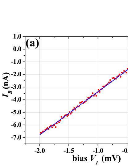
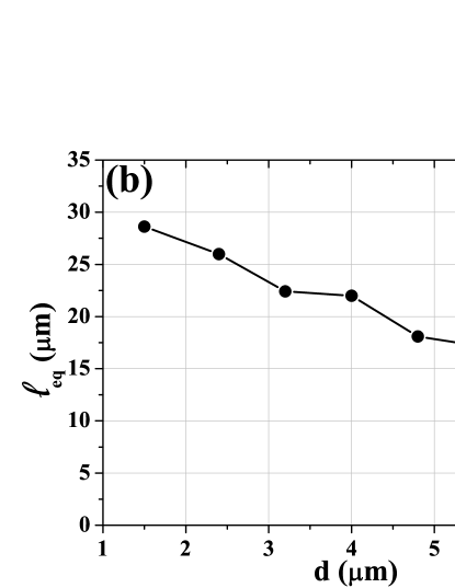
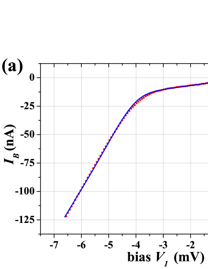
Figure 4(a) shows the - characteristics (red dots) for the m case. The behavior is clearly ohmic, as confirmed by a linear fit (blue line, adjusted ). This agrees with the predictions of our model for low bias, when radiative emission is negligible and Eq. 8 applies. The zero-bias differential conductance depends on the distribution of scattering centers inside the constriction. Equation 8 allows us to obtain the equilibration length by fitting the - curves in the linear region. Figure 4(b) displays the different values obtained for each junction length . The average value (21 m) is consistent with the one reported in Ref. Paradiso2011, (15 m), considering that those results were obtained from different samples. The graph evidences that depends on . As shown in Ref. Paradiso2011, , the actual impurity density is highly sample-dependent and can fluctuate along the inter-channel junction. The monotonical decrease observed in Fig. 4(b) could however indicate that for short the scattering centers are somewhat less effective, due to the fact that the edges are smoothly brought into interaction and separated. Therefore the inter-channel separation is larger at the constriction ends than at the inner points. These boundary effects are more important for smaller .
The previous results provide the first of the two free parameters of our model, namely and . Therefore we fit the experimental curves in Fig. 2 with the functions obtained solving Eqs. 3 and 13, with the only free parameter . The fit for m is displayed in Fig. 5(a), together with the experimental data. The agreement between the two curves is remarkable: our simple model reproduces both the shift and the smoothing at the threshold, i.e. the two main features observed in Fig. 2. The threshold shift can be better seen in Fig. 5(b), where we plot the fits for all experimental curves of Fig. 2 (solid lines), together with the corresponding experimental data (dotted lines). In the inset we show a comparison between the threshold voltage values extracted from the fitting curves and the ones directly estimated from the - characteristics. This graph clearly indicates that the present model suitably describes the observed threshold reduction. The value for the Landau level gap ( meV) was kept constant in these fits. This value turns out to be optimal once both and have been determined, because then a further adjustment of the gap only decreases the fit quality.
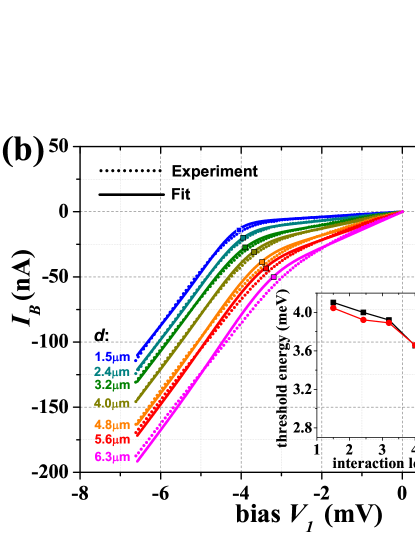
This result explains the reduction of the threshold for photon emission observed in several experiments.Ikushima2010 ; Wurtz2002 The significant deviation from is an effect due to the electron heating induced by the injection of hot carriers in the outer edge via elastic scattering.
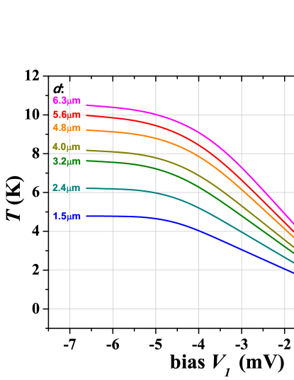
To quantitatively estimate the electron temperature increase, we solved Eq. 13, using the parameters and provided by the previous fits, with the initial condition mK. Figure 6 shows the solutions for the values corresponding to the experimental data in Fig. 2. For very small bias the temperature increases almost quadratically with the imbalance, while for intermediate values the behavior is approximatively linear, with a slope proportional to . Finally, the temperature tends to saturate at the onset of radiative emission, which suppresses further injection of hot electrons into the outer edge. At saturation, the output edge temperatures are by far larger than the base temperature.
In section III we considered a linear edge dispersion, which neglects effects of edge reconstruction due to electron-electron interaction.Chklovskii1992 We have also developed alternative models, which take into account the effect of the compressible and incompressible stripes at the sample edge. While such more complex analysis correctly predicts the linear behavior at low bias, it is less satisfactory in describing the threshold evolution, although it contains more adjustable parameters (as the compressible and incompressible stripe widths). We interpreted such discrepancy as the effect of the high electron temperature induced by the elastic scattering processes and present on most part of the edge junction. As edge reconstruction is known to be quickly washed out by temperature,Machida1996 ; Lier1994 ; Suzuki1993 we have therefore rather chosen a simple model with a linear edge dispersion, which indeed captures the relevant features observed in the experiment.
V Conclusion
We demonstrated a tunable-length junction between highly imbalanced edge channels in the quantum Hall regime. The measurements of its current-voltage characteristics clearly evidence that the threshold voltage for the onset of radiative emission depends on the junction length . We show how this behavior can be explained by a simple model accounting for the heating effect due to the elastic scattering of hot carriers.
Acknowledgements.
We acknowledge financial support from the Italian Ministry of Research (MIUR-FIRB projects RBIN045MNB, RBIN048ABS, RBID08B3FM, RBIN067A39_002, and RBIN06JB4C).Appendix A Integration of expressions containing Fermi functions
In Eq. 6 we evaluated the integral
| (14) |
Defining , and , we have
| (15) |
A primitive of the expression in brackets is
| (16) |
thus
| (17) | |||||
In Eq. 10 we evaluated the integral
| (18) |
Defining , and , we have
| (19) |
A primitive of the expression in square brackets is
| (20) |
thus
| (21) | |||||
Appendix B First order approximation to the edge energy
Appendix C Determination of
When the electron temperature is non-zero, the expression for the total edge energy has an extra term proportional to , as seen in Eq. 23. We can thus define the electrostatic and the thermal component of the total edge energy:
| (24) |
where is the edge voltage referred to the ground.
References
- (1) B. I. Halperin, Phys. Rev. B 25, 2185 (1982).
- (2) N. Paradiso, S. Heun, S. Roddaro, L. N. Pfeiffer, K. W. West, L. Sorba, G. Biasiol, and F. Beltram, Physica E 42, 1038 (2010).
- (3) F. E. Camino, W. Zhou, and V. J. Goldman, Phys. Rev. Lett. 95, 246802 (2005).
- (4) Y. Ji, Y. Chung, D. Sprinzak, M. Heiblum, D. Mahalu, and H. Shtrikman, Nature 422, 415 (2003).
- (5) I. Neder, M. Heiblum, Y. Levinson, D. Mahalu, and V. Umansky, Phys. Rev. Lett. 96, 016804 (2006).
- (6) I. Neder, F. Marquardt, M. Heiblum, D. Mahalu, and V. Umansky, Nat. Phys. 3, 534 (2007).
- (7) P. Roulleau, F. Portier, D. C. Glattli, P. Roche, A. Cavanna, G. Faini, U. Gennser, and D. Mailly, Phys. Rev. B 76, 161309(R) (2007).
- (8) S. Roddaro, V. Pellegrini, F. Beltram, G. Biasiol, L. Sorba, R. Raimondi, and G. Vignale, Phys. Rev. Lett. 90, 046805 (2003).
- (9) S. Roddaro, V. Pellegrini, F. Beltram, G. Biasiol, and L. Sorba, Phys. Rev. Lett. 93, 046801 (2004).
- (10) S. Roddaro, V. Pellegrini, F. Beltram, L. N. Pfeiffer, and K. W. West, Phys. Rev. Lett. 95, 156804 (2005).
- (11) S. Roddaro, N. Paradiso, V. Pellegrini, G. Biasiol, L. Sorba, and Fabio Beltram, Phys. Rev. Lett. 103, 016802 (2009).
- (12) C. Altimiras, H. le Sueur, U. Gennser, A. Cavanna, D. Mailly, and F. Pierre, Nature Phys. 6, 34 (2010).
- (13) I. Neder, N. Ofek, Y. Chung, M. Heiblum, D. Mahalu, and V. Umansky, Nature 448, 333 (2007).
- (14) A. Würtz, R. Wildfeuer, A. Lorke, E. V. Deviatov, and V. T. Dolgopolov, Phys. Rev. B 65, 075303 (2002).
- (15) T. Nakajima, Y. Kobayashi, S. Komiyama, M. Tsuboi, and T. Machida, Phys. Rev. B 81, 085322 (2010).
- (16) N. Paradiso, S. Heun, S. Roddaro, D. Venturelli, F. Taddei, V. Giovannetti, R. Fazio, G. Biasiol, L. Sorba, and F. Beltram, Phys. Rev. B 83, 155305 (2011).
- (17) S. Komiyama, H. Hirai, S. Sasa, and S. Hiyamizu, Phys. Rev. B 40, 12566 (1989).
- (18) S. Komiyama, H. Hirai, M. Ohsawa, Y. Matsuda, S. Sasa, and T. Fujii, Phys. Rev. B 45, 11085 (1992).
- (19) K. Ikushima, H. Sakuma, S. Komiyama, and K. Hirakawa, Phys. Rev. B 76, 165323 (2007).
- (20) K. Ikushima, D. Asaoka, S. Komiyama, T. Ueda, K. Hirakawa, Physica E 42, 1034 (2010).
- (21) T. Machida, H. Hirai, S. Komiyama, T. Osada, and Y. Shiraki, Phys. Rev. B 54, R14261 (1996).
- (22) S. Komiyama, H. Sakuma, K. Ikushima, and K. Hirakawa, Phys. Rev. B 73, 045333 (2006).
- (23) The analysis of this behavior, already observed in other experiments,Wurtz2002 is beyond the scope of the present paper.
- (24) G. Müller, D. Weiss, A. V. Khaetskii, K. von Klitzing, S. Koch, H. Nickel, W. Schlapp, and R. Lösch, Phys. Rev. B 45, 3932 (1992).
- (25) D. B. Chklovskii, B. I. Shklovskii, and L. I. Glazman, Phys. Rev. B 46, 4026 (1992).
- (26) K. Lier and R. R. Gerhardts, Phys. Rev. B 50, 7757 (1994).
- (27) T. Suzuki and T. Ando, J. Phys. Soc. Jpn. 62, 2986 (1993).