Spintronic devices on the base of magnetic nanostructures
L.V. Lutsev, A.I. Stognij *, N.N. Novitskii *, and A.S. Shulenkov **
A.F. Ioffe Physical-Technical Institute, Russian Academy of
Sciences, 194021, St Petersburg, Russia
∗ Scientific
and Practical Materials Research Center, National Academy of
Sciences of Belarus, 220072 Minsk, Belarus
∗∗ Minsk
Research Institute of Radiomaterials, 220074, Minsk, Belarus
E-mail: l_lutsev@mail.ru
Abstract
Two types of spintronic devices on the base of magnetic nanostructures containing silicon dioxide films with cobalt nanoparticles SiO2(Co) on GaAs substrate – magnetic sensors and field-effect transistor governed by applied magnetic field – are studied. Magnetic sensors are based on the injection magnetoresistance effect. This effect manifests itself in avalanche suppression by the magnetic field in GaAs near the SiO2(Co)/GaAs interface. Field-effect transistor contains the SiO2(Co) film under gate. It is found that the magnetic field action leads to great changes in electron mobility in the channel due to the interaction between spins of Co nanoparticles and electron spins.
1 Introduction
Manipulation of carrier spins in ferromagnetic / semiconductor heterostructures offers enhanced functionality of spin-electronic devices such as spin transistors, sensors, and magnetic memory cells [1, 2]. This manipulation can be realized on the base of magnetic nanostructures by use of magnetoresistance effects and due to interactions between magnetic nanostructures and electron spins in field-effect transistors. Magnetoresistance effects are attracting much attention in a view of their various applications. An extremely large magnetoresistance ( %) has been observed at room temperature in GaAs / granular film heterostructures in the avalanche state, where a granular film contains ferromagnetic metal nanoparticles or ferromagnetic islands on the semiconductor / film interface. The value of this effect is two-three orders higher than the maximum values of the giant magnetoresistance in the metal magnetic multilayers and the tunnelling magnetoresistance in the magnetic tunnel junction structures. Magnetoresistance effects of high values have been found in GaAs / granular film heterostructures with granular films containing ferromagnetic metal MnSb nano-islands [3, 4] and ferromagnetic MnAs clusters [5]. The high values of the magnetoresistance based on the avalanche breakdown has been observed on the SiO2(Co)/GaAs heterostructures, where the SiO2(Co) is the granular SiO2 film containing Co nanoparticles [6, 7, 8, 9]. This effect has been called the injection magnetoresistance (IMR). It appears, when electrons are injected from the granular film into the GaAs.
Field-effect HEMT devices with spin polarized electron channels are perspective due to the possibility to change electron spins in channels by a magnetic field action. In this paper, we study devices on the base of magnetic nanostructures with silicon dioxide films with cobalt nanoparticles SiO2(Co) on GaAs substrate – magnetic sensors and field-effect transistor governed by applied magnetic field. Magnetic sensors are based on the IMR effect. The field-effect transistor contains the SiO2(Co) film under gate. The magnetic field action leads to great changes in the electron mobility in the channel due to the interaction between spins of Co nanoparticles and electron spins.
2 Giant injection magnetoresistance and magnetic sensors
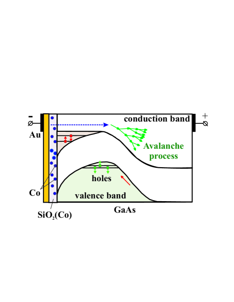
High values of the IMR-effect in the SiO2(Co) heterostructures are explained by the magnetic-field-controlled process of impact ionization in the vicinity of the spin-dependent potential barrier formed in the semiconductor (Fig. 1). The spin-dependent potential barrier is formed near the interface by the exchange interaction between the electrons in localized states in the electron accumulation layer in the semiconductor and -electrons of Co [8, 10]. The avalanche process is induced by electrons, which (1) surmount over the spin-dependent potential barrier formed by the exchange-splitted localized states and (2) tunnel from the localized states. The impact ionization induced by the injected electrons produces holes, which move, are accumulated in the region of the potential barrier and lower the barrier height [8]. Owing to the formed hole feedback, small variations in the barrier height lead to great changes in the current and in the avalanche process. The applied magnetic field increases the barrier height, reduces the transparency of the barrier, and suppresses the onset of the impact ionization.
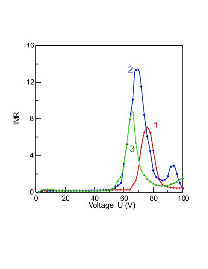
Magnetic sensors were performed on the samples SiO2(Co)/GaAs with the -GaAs substrates. Carrier concentrations in the -GaAs are equal to cm-3. The SiO2(Co) films were deposited by the ion-beam co-sputtering of the composite cobalt-quartz target onto the GaAs substrates heated to 200∘C. The concentration of Co nanoparticles in the silicon dioxide was varied by changing the ratio of target areas of cobalt and quartz areas. The film composition was determined by the nuclear physical methods of element analysis using a deuteron beam of the electrostatic accelerator (Rutherford backscattering spectrometry and nuclear reaction with oxygen). For the samples used in magnetic sensors, the relative Co content is in the range 45 - 71 at.% and the film thickness is 40 nm. The average size of Co particles, determined from the low-angle X-ray scattering measurements, increases with Co content: from 2.9 nm at 45 at.% to 3.9 nm at 71 at.%. As the Co content increases, the resistivity of the SiO2(Co) films decreases from 0.3 cm (45 at.%) through 3.0 cm (60 at.%) to 1.4 cm (71 at.%). The protective Au layer of the thickness 3 - 5 nm have been sputtered on the SiO2(Co) films.
The sizes of the samples in magnetic sensors were equal to mm. One contact was on the GaAs substrate, and the other – on the Au layer sputtered on the granular film. Magnetic sensors are characterized by the injection magnetoresistance, which is defined by the coefficient
where and are the resistances of the SiO2(Co)/GaAs heterostructure without a field and in the magnetic field , respectively; and are the current densities flowing in the heterostructure in the absence of a magnetic field and in the field . The IMR ratio for SiO2(Co)/GaAs heterostructures with different Co concentrations versus the applied voltage in the magnetic field = 2.1 kOe at room temperature is shown in Fig. 2. The magnetic field is parallel to the film. According to [8], for magnetic fields of high values ( 10 kOe) the IMR coefficient increases with the growth of the applied voltage. In contrast to this, for low magnetic fields the IMR reaches highest values in the region of the avalanche onset. As one can see from Fig. 2, in order to reach high sensitivity of sensors it is need to apply the voltage in this region.
3 Field-effect transistor governed by magnetic field
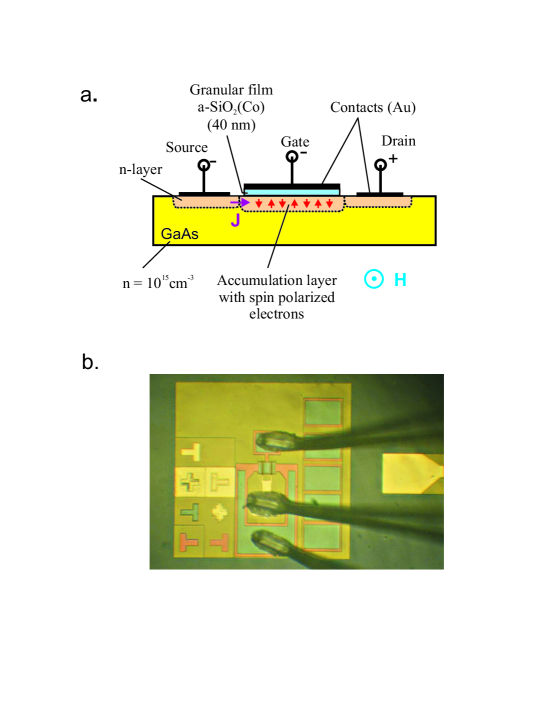
The field-effect HEMT device with a spin polarized electron channel was developed on the base of the -GaAs/AlGaAs heterostructures (Fig. 3). This device contains an amorphous granular SiO2(Co) film with cobalt nanoparticles under the gate electrode. The thickness of the film is equal to 40 nm. The SiO2(Co) film polarizes electron spins in the accumulation layer under the gate.
Current-voltage curves of field-effect devices have two different parts [11]. If the voltage between the source and the drain is less than the saturation voltage , then the current-voltage curve is sub-linear and the current flowing in the channel is written as
| (1) |
where is the voltage between the gate and the source, is the threshold voltage between the gate and the source, when there is no current in the channel, is the specific capacity between the gate and the channel, is the electron mobility, and are the channel width and the length, respectively. When , the channel becomes blocked at the drain contact and an electrical field of high value appears in this region. In this case, the saturation voltage is
For the drain current is weakly dependent on the voltage and the current-voltage curve can be approximated by a line with a weak slope. In the first approximation this sloping part of the current-voltage curve can be written as
| (2) |
The current-voltage dependences of the developed field-effect HEMT structure (Fig. 4) contain two parts of the current-voltage curve described by relations (1) and (2). The saturation voltage is in the range 0.4 - 0.7 mV. As one can see from Fig. 4, the drain current of the field-effect transistor presents strong dependence on the governed external magnetic field . The electron mobility in the channel decreases with the growth of the applied magnetic field. This property can be used in magneto-sensitive devices.

4 Conclusions
We study devices on the base of magnetic nanostructures containing silicon dioxide films with cobalt nanoparticles SiO2(Co) on GaAs substrate – magnetic sensors and field-effect transistor. Magnetic sensors are based on the injection magnetoresistance effect in the avalanche onset regime. The field-effect transistor contains SiO2(Co) film under gate. The both structures exhibit high magnetic sensitivity at room temperature.
Acknowledgments
The authors gratefully acknowledge the assistance of Dr. V.M. Lebedev (PNPI, Gatchina, Leningrad region, Russia) for determination of the film composition. This work was supported by the Russian Foundation for Basic Research, grant 10-02-00516, and by the Ministry of Education and Science of the Russian Federation, project 2011-1.3-513-067-006.
References
- [1] S. A. Wolf, D. D. Awschalom, R. A. Buhrman et al., Science 294, 1488 (2001).
- [2] G. Schmidt, J. Phys. D 38, R107 (2005).
- [3] H. Akinaga, M. Mizuguchi, K. Ono et al., Applied Physics Letters 76, 357 (2000).
- [4] H. Akinaga, Semicond. Sci. Technol. 17, 322 (2002).
- [5] 5. M. Yokoyama, T. Ogawa, A.M. Nazmul et al., J. Appl. Phys. 99, 08D502 (2006).
- [6] L.V. Lutsev, A.I. Stognij, and N.N. Novitskii, JETP Letters 81, 514 (2005).
- [7] L.V. Lutsev, A.I. Stognij, N.N. Novitskii et al., J. Magn. Magn. Mat. 300, e12 (2006).
- [8] L.V. Lutsev, A.I. Stognij, and N.N. Novitskii, Phys. Rev. B 80, 184423 (2009).
- [9] L.V. Lutsev, A.I. Stognij, N.N. Novitskii et al., Solid State Phenomena 168-169, 23 (2011).
- [10] L.V. Lutsev, J. Phys.: Condensed Matter 18, 5881 (2006).
- [11] V.V. Pasynkov, L.K., Chirkin, and A.D. Shinkov, Semiconductor Devices. Vyshaya Shkola, Moscow (1981) [in Russian].