Semiconducting graphene nanomeshes
Abstract
Symmetry arguments are used to describe all possible two-dimensional periodic corrugations of graphene (“nanomeshes”) capable of inducing tangible semiconducting gap. Such nanomeshes or superlattices break the initial graphene translational symmetry in a way that produces mixing and subsequent splitting of the Dirac and states. All of them have hexagonal Bravais lattice and are described by space groups that are subgroups of the graphene group. The first-principles calculations show that the gaps of about 0.5 eV can be induced at strains safely smaller than the graphene failure strain.
pacs:
73.22.Pr, 81.05.ue, 62.25.-gGraphene, a truly two-dimensional crystal of carbon atoms with a honeycomb lattice, exhibits giant carrier mobilities up to cm2/Vs bolotin ; morozov ; dusari2011 , it has a record mechanical strength with critical deformations exceeding 20% and huge thermal conductivity reaching 1800 WK-1m-1leeThrmlG . As such, it is very promising as a circuit material in electronic devices. However, the absence of a band gap in graphene prevents its immediate use as e.g. a channel in switchable devices like field effect transistors.
Perhaps, the most straightforward way to induce a gap in graphene is through quantum confinement - one should simply cut a graphene sheet into small pieces like nanoribbons berger ; han or dots ponomarenko . However, it is difficult to control the band gap produced in such a way because it strongly depends on the size and edge geometry of the nanostructures. That is why many papers have been focused on the opening up a spectral gap in a ‘bulk’ material using different kinds of periodic lattice perturbations with various substrates zhou ; gioavannetti , antidot lattices yu ; vanevic ; liu ; baskin , regular lines or areas of adsorbed foreign atoms chernozatonskii ; ito ; balog ; xu , external periodic electric and magnetic fields snyman , laser field savel'ev , Kekulé distortions lee , etc.
Mechanical out-of-plane sine-wave deformations certainly belong to this class of perturbations. Recently, we showed that the one-dimensional (1D) periodic ripples can open a gap at the Dirac points only due to (i) breaking of the inversion symmetry or equivalency between A and B sublattices and/or (ii) merging of two inequivalent Dirac points, and naubra1d . Breaking of inversion symmetry was found to have only a relatively modest contribution to the gap, especially when the amplitude of a sine wave deformation is relatively small in comparison with the period . A tangible gap can mainly result from mutual annihilation of the Dirac points and , yet this requires severe corrugations.
Importantly, in the case of 1D periodic corrugations the energy gap at the Fermi level cannot be induced due to mixing of electronic states belonging to two different valleys (or to two inequivalent Dirac points and in the unperturbed graphene) even if the imposed period provides a momentum transfer coupling the Dirac points. The reason is that the Dirac points generally shift from their initial positions as the amplitude of corrugations increases, so that the relation does not hold any longer at any finite amplitude .
In the present study, we show that in contrast to 1D the 2D out of plane modulations can easily induce the gap at the Dirac points via mixing, provided that the modulations have hexagonal translational symmetry. It might appear that this idea falls under the concept developed in Ref. pacoNP10 of creating the gaps in graphene by putting the latter on top of a corrugated surface with a triangular landscape. In reality, however, there is nothing in common between the two since we consider the semiconducting gaps forming at the Dirac points due to inter-valley mixing, while the authors pacoNP10 studied the multiple minigaps lying above (and below) the Dirac energies.
The opportunity to open up the gap through 2D corrugations has become especially interesting in light of the recent experiments showing that such corrugations (”nanomeshes”) can be formed during the epitaxial graphene growth on some special substrates like SiC(0001) emtsev ; kim1 ; riedl ; qi or transition metal surfaces preobrajenski ; martoccia ; ma . When grown, for example, on Ru(0001), graphene forms a nanomesh where carbon hexagons are commensurate with unit cells of Ru martoccia .
In what follows, we consider a graphene sheet with 2D corrugated profile that forms either due to a lattice misfit with a substrate or follows its surface corrugation. In order to mix the unperturbed and Bloch states, such a profile should break the initial translational symmetry in such a way that both points and are translated into the origin (point) within the new “folded” Brillouin zone (BZ). Clearly, this can be achieved only if a deformed graphene sheet that (i) still has a hexagonal Bravais lattice with the angle between two primitive super-periods of equal length, and , and (ii) its first reciprocal lattice vectors with the same length, and , are specifically commensurate with the vectors and . As to requirement (i), it is easy to list all the hexagonal superlattices that are commensurate with the graphene honeycomb lattice. Indeed, their periods are , , where and are arbitrary integers, and are the initial graphene periods. Accordingly, their reciprocal vectors defined through the corresponding graphene vectors are: , , where ; and .
From all possible hexagonal superlattices discussed above, not all satisfy the condition (ii), but only those where is the multiple of three guinea . Interestingly, in 1D case of carbon nanotubes this is a condition of their gapless (metallic) behavior, while in the present 2D cases it facilitates opening up the gap, as we discuss below. Such structures, capable of mapping the graphene and points to the point, can be divided in three classes: zigzag, armchair, and chiral, depending on the directions of . For the zigzag superlattices, , so that the periods and are parallel to two different zigzag directions. This type of superstructures can also be referred to as , where is an integer. In the case of armchair-edged corrugations, . Here, the super-periods are rotated by 30∘ relative to the graphene vectors and . Since the length of the super-periods is larger than that in graphene by a factor of , the structures themselves can be labeled as . And, finally, the chiral superlattices can also be referred to as .
It is worth noticing that the superstructure breaks the initial translation symmetry in the same way as so-called Kekulé distortion does, where the in-plane atomic displacements can be viewed as a frozen symmetrized combination of transverse optical phonon modes at -points lee ; gunlycke . While the Kekulé distortion does not break the point group symmetry of the system, D6h, this is not the case for all out-of plane 2D corrugations considered here. Indeed, introducing sine-like corrugations kills at least the horizontal mirror plane, , and the resulting point group is inevitably lower than D6h (actually it can be one of its subgroups: C6v, D6, C6, S6, D3d, C3v, D3 or C3 milosevic ).
All three classes of periodic ripples, in their simplest form, can be modeled by the out-of-plane atomic displacements
| (1) |
where are the undistorted lattice positions, is the amplitude, are the first supercell equal-length reciprocal lattice vectors, each rotated by with respect to one another, is the origin of the coordinate system, and some phase. Below, we will characterize the amplitude via a dimensionless ratio , where is the length of a super-period; . Note that the sum of two exponents in Eq. (1) reduces to the cosine function when , and to the sine function when .
The displacement field , Eq. (1), leads to a strain field (quadratic in since the linear terms vanish)
| (2) |
which is also periodic and has non-zero Fourier components of the type . Since such a strain modulates the interatomic hopping integrals, the electrons of the superlattice should “feel” strongly not only the components of the potential with the smallest vectors , but also those with . This, in turn, should promote the gap opening due to enhancing of the second and higher order diffraction effects.
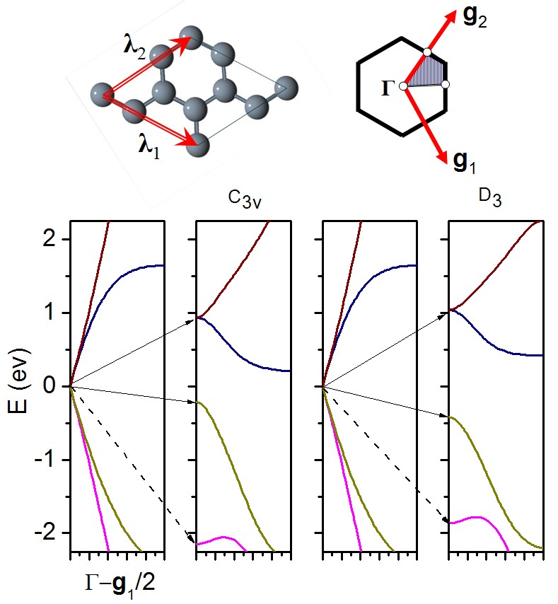
The resulting point symmetry of a superstructure imposed by Eq. (1) depends on a choice of the origin and phase . Table 1 lists, for example, the symmetries corresponding to two choices of - either in the center of a hexagon or on a carbon atom - and two choices of : and . Although all the superstructures listed in Table 1 have identical in shape (hexagonal) BZs, the irreducible part of the latter can differ in going from one structure to another. Thus, the irreducible part for the C6v and D3d superlattices is geometrically identical to that for graphene, whereas for C6, S6, C3v and D3 is twice and for C3 four time larger than that for graphene milosevic . For the C6v and D3d structures, we denote the high-symmetry points at the corners of the superlattice BZ as Ks, and at centers of the edges as Ms, Fig. 1.
. center of hexagon carbon atom C6v C3v D3d C3v C6v (1) C3v /2 D3d(1) D3 C6 C3 /2 S6 C3
To illustrate the suggested concept, we have performed band structure calculations for the corrugated graphene sheets using density functional theory implemented in the ABINIT package abinit (for computational details, see Supplemental Material LABEL:sec:suppl.) Among the groups listed in Table 1, only C6v, D3d, C6 and S6 contain the symmetry elements that interchange the A and B sublattices. For such groups, the gap opens up solely due to inter-valley mixing: the distortion breaks the 4-fold degeneracy at point of a flat graphene into two 2-fold degeneracies. In the case of armchair C6v and D3d superlattices, the gap reaches substantial values of 0.33 and 0.30 eV, respectively, as the increases from to (Fig. 1). With the constraint , these values are reduced by a factor of three in passing to the armchair superlattices having the same symmetries. They are further reduced by a factor in going to the chiral C6 and S6 structures corresponding to and . Clearly, this progressive narrowing of the gap is due to increasing period , because the ratio remains the same.

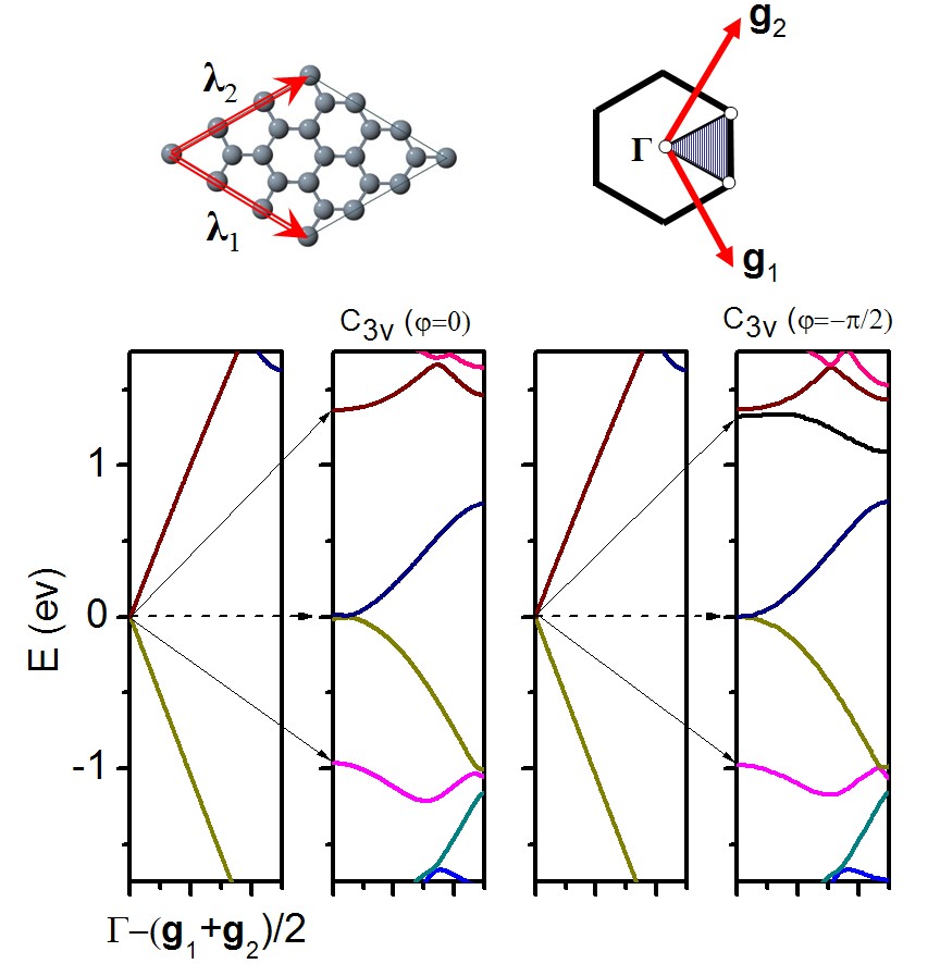
The corrugations associated with the symmetries C3v, D3 and C3 (Table 1) break not only the translational but also the sublattice symmetry. In such an event, both the inter-valley and intra-valley mixing effects contribute to the reconstruction of the band structure in the vicinity of the Fermi level. In the case of armchair C3v and D3 structures, for example, the four-fold degenerate state at splits into two single levels and a two-fold degenerate state, Fig. 2. The 2-fold degenerate state is above the Fermi level, so that the gap opens up and becomes indirect when the exceeds some critical value (as in Fig. 2). Although in the zigzag C3v superlattices the 4-fold degenerate state also splits into three states, here the two-fold degenerate state lies between the two single levels and the gap does not open up at all, Fig. 3. This result is quite unexpected, it shows that breaking the inversion symmetry is not a sufficient condition for the gap opening. Note that the principal possibility for graphene lattice to have zero energy gap in the absence of inversion symmetry was discussed earlier in Ref. kishigi .
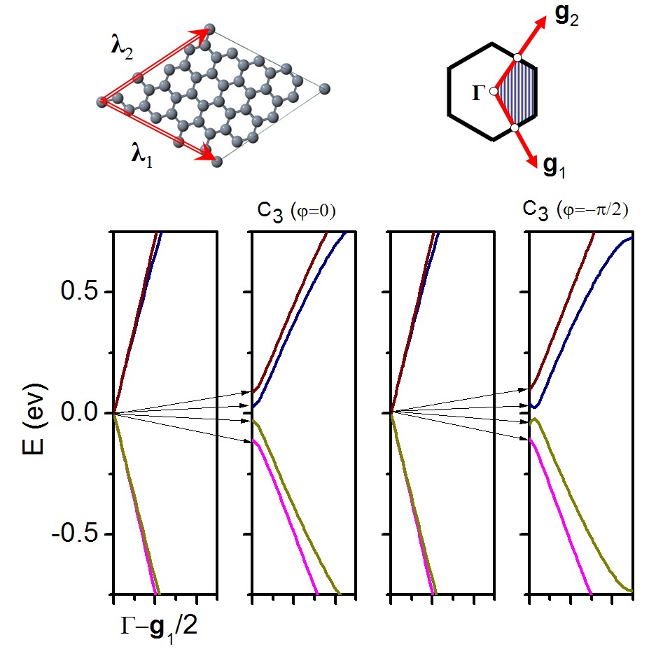
It is interesting that in going over from to structures with the same point symmetries (C3v and D3), the character of splitting of the 4-fold degenerate state remains but only for very small corrugation parameters . As the is further increased, the 2-fold degeneracy is lifted and the structures exhibits four single levels. We should stress that if only the lowest order effects of the corrugations were considered (quadratic in ), the splitting of the four-degenerate level would follow the ratios obtained from symmetry considerations. In the present calculations, however, the effects of corrugation are included up to an infinite order, so that the character of splitting is not in one-to-one correspondence with the symmetry of deformed structures. The 4-fold degeneracy is completely lifted at any for the chiral superlattices with C3 symmetries, as exemplified by the C3 structure in Fig. 4. Here, a modest gap on the order of 0.1 eV opens up as reaches . Note that once the gap is opened at , it does not necessarily remains the direct gap, the conduction band minimum may move around in the BZ, and the gap may become indirect, as it is seen from the Fig. 4 for the case . The above results provide exhaustive classification of possible scenarios for gap opening in graphene subject to the two-dimensional corrugation. It would be interesting to check the above predictions in experiments with various substrates producing planar corrugations of a top graphene layer.
Supplement: Calculation Method. The DFT calculations for both flat and corrugated graphene have been performed using ABINIT abinit within the local density (LDA) approximation. Approximately the same k-point density for Monkhorst-Pack -point grid kpts was used for all superstructures; roughly it corresponds to a 16161 grid for a flat graphene with 2 atoms per unit cell. The sheets have been simulated by a slab-supercell approach with the inter-planar distances of to ensure negligible wave function overlap between the replica sheets. The plane waves pseudopotentials have been chosen in the form of Troullier-Martins trou91 where carbon 2s and 2p electrons have been considered as valence states. For the plane-wave expansion of the valence and conduction band wave-functions, a cutoff energy was chosen to be 80 Ry.
References
- (1) K. I. Bolotin et al., Solid State Comm. 146, 351 (2008).
- (2) S. V. Morozov et al., Phys. Rev. Lett. 100, 016602 (2008).
- (3) S. Dusari, J. Barzola-Quiquia, P. Esquinazi, and N. Garcia, Phys. Rev. B 83, 125402 (2011).
- (4) J.-U. Lee, D. Yoon, H. Kim, S.W. Lee, and H. Cheong, Phys. Rev. B 83, 081419(R) (2011).
- (5) C. Berger et al., Science 312, 1191 (2006).
- (6) M. Y. Han, B. Ozyilmaz, Y. Zhang, P. Kim, Phys. Rev. Lett. 98, 206805 (2007).
- (7) L.A. Ponomarenko et al., Science 320, 356 (2008).
- (8) S. Y. Zhou et al., Nature Mat. 6, 770 (2007).
- (9) G. Giovannetti, P.A. Khomyakov, G. Brocks, P.J. Kelly, J. van den Brink, Phys. Rev. B 76, 073103 (2007).
- (10) D. Yu et al., Nano Res. 1, 56 (2008).
- (11) M. Vanević, V. M. Stojanović, and M. Kindermann, Phys. Rev. B 80, 045410 (2009).
- (12) W. Liu, Z.F. Wang, Q. W. Shi, J. Yang, and F. Liu, Phys. Rev. B 80, 233405 (2009)
- (13) A. Baskin and P. Král, Nature Sci. Reports 1, 36 (2011).
- (14) L. A. Chernozatonskii et al., JETP Letters 85, 77 (2007).
- (15) J. Ito and A. Natori, J. Appl. Phys. 103, 113712 (2008).
- (16) R. Balog et al., Nature Mat. 9, 315 (2010).
- (17) Z. Xu and K. Xue, Nanotechnology 21, 045704 (2010).
- (18) I. Snyman, Phys. Rev. B 80, 054303 (2009).
- (19) S. E. Savel’ev and A.S. Alexandrov, Phys. Rev. B 84, 035428 (2011).
- (20) S.-H. Lee et al. ACS Nano 5, 2964 (2011).
- (21) I.I. Naumov and A.M. Bratkovsky, arXiv:1104.0314v1 [cond-mat.mes-hall].
- (22) F. Guinea, M. I. Katsnelson, and A. K. Geim, Nature Phys. 6, 30 (2010).
- (23) K. V. Emtsev, F. Speck, Th. Seyller, L. Ley, and J.D. Riley, Phys. Rev. B 77, 155303 (2008).
- (24) S. Kim, J. Ihm, H. J. Choi, and Y.-W. Son, Phys. Rev. Lett. 100, 176802 (2008).
- (25) C. Riedl, C. Coletti and U. Starke, J. Phys. D 43, 374009 (2010).
- (26) Y. Qi, S. H. Rhim, G. F. Sun, M. Weinert, and L. Li, Phys. Rev. Lett. 105, 085502 (2010).
- (27) A. B. Preobrajenski, M. L. Ng, A. S. Vinogradov, and N. Mårtensson, Phys. Rev. B 78, 073401 (2008).
- (28) D. Martoccia, et al., Phys. Rev. Lett. 101, 126102 (2008).
- (29) H.-F. Ma, M. Thomann, J. Schmidlin, S. Roth, M. Morscher, and T. Greber, Front. Phys. China 5, 387 (2010).
- (30) F. Guinea and T. Low, Phil. Trans. R. Soc. A 368 5391 (2010)
- (31) D. Gunlycke, H.M. Lawler and C. T. White, Phys. Rev. B 75, 085418 (2007).
- (32) I. Milos̆ević, B. Nikolić, M. Damnjanović and M. Krc̆marz, J. Phys. A 31,3625 (1998).
- (33) K. Kishigi, R. Takeda, and Y. Hasegawa, J. Phys. Conf. Ser. 132, 101205 (2005).
- (34) X. Gonze et al., Comp. Mater. Sci. 25, 478 (2002).
- (35) H. J. Monkhorst and J. D. Pack, Phys. Rev. B 13, 5188 (1976).
- (36) N. Troullier and J. L. Martins, Phys. Rev. B 43, 1993 (1991).