VO2 nanosheets: controlling the THz properties through strain engineering
Abstract
We investigate far-infrared properties of strain engineered vanadium dioxide nanosheets through epitaxial growth on a (100)R TiO2 substrate. The nanosheets exhibit large uniaxial strain leading to highly uniform and oriented cracks along the rutile c-axis. Dramatic anisotropy arises for both the metal-insulator transition temperature, which is different from the structural transition temperature along the cR axis, and the metallic state conductivity. Detailed analysis reveals a Mott-Hubbard like behavior along the rutile cR axis.
§contributed equally to this work
I. INTRODUCTION
During the past five decades, vanadates have been intensely investigated from the point of view of clarifying the physics of metal-insulator transitions (MIT). Vanadium dioxide (VO2) is particularly intriguing, exhibiting a MIT with a conductivity decrease of over five orders of magnitude Ladd1969 . This is accompanied by a transition from a high temperature metallic rutile structure to an insulating monoclinic structure below the transition temperature. In bulk, the structural transition temperature, , equals the metal-insulator transition temperature, , i.e. Andersson1956 . However, VO2 is not yet fully understood regarding the Mott-Hubbard or Peierls like nature of its MIT, though it is now generally accepted that a complete description requires explicit consideration of electron-electron correlations Biermann2005 ; Lazarovits2010 . This is motivated in particular by the observed difference between the MIT and the structural transition temperatures, which provides significant evidence that the correlated conductivity behavior is independent of the structural phase Kim2006 ; Qazilbash2011 ; Arcangeletti2007 . Additionally, recent experimental studies highlight the multifunctional potential of VO2 including current or photoinduced phase changes (with the commensurate large tuning of the dielectric function) as well as integration with other technologies for applications including light detection and memory-based metamaterials Kim2005 ; Driscoll2009 ; Hilton2007 .
Strain engineering enables an additional degree of control of technologically relevant properties and provides a discriminatory capability towards obtaining fundamental insight into the microscopic origin of the macroscopic characteristics. Strain has been used to modify the MIT temperature in VO2 through direct application Muraoka2002 or substrate-dependent application Lu2008 ; Zhang2009 of stress. For the present measurements, we utilize highly strained epitaxial (100)R VO2 thin films. The far-infrared conductivity is measured using non-contact polarization sensitive terahertz time-domain spectroscopy (THz-TDS) providing direct access to the coherent quasiparticle response along bR or cR by simply changing the sample orientation. Subsequent analysis indicates that the strain engineered tuning of vanadium and orbitals controls the MIT transition temperature along cR, which is different from the structural transition temperature. The origin of the observed conductivity anisotropy is also discussed, along with the potential for a technological application of strain engineered VO2 thin films as temperature switched far-infrared polarizers.
II. EXPERIMENTS
The and thick VO2 films we investigated were deposited on rutile (100)R TiO2 substrates by temperature optimized sputtering from a vanadium target, using the reactive bias target ion beam deposition technique in an Ar+O2 gas mixture; details of the growth conditions can be found elsewhere West2008 . The samples morphology was characterized by optical, atomic force (AFM) and scanning electron microscopies (SEM), and the film microsctructure was analyzed by temperature dependent X-ray diffraction (XRD).
THz-TDS is a non-contact method to measure far-infrared conductivity. The conductivity anisotropy is easily determined from transmission of THz pulses for different sample orientations. In our case the output of a 1kHz 35fs Ti:Sapphire amplifier is used to generate nearly single-cycle THz pulses via optical rectification in a ZnTe crystal. We then employ a standard THz Time Domain Spectroscopy (THz TDS) setup to measure the transmission in the THz frequency range THz Jepsen2011 . By changing the sample orientation with respect to the THz pulse polarization we are able to monitor the transmission along different crystal axes.
(100)R TiO2 has a large refractive index anisotropy in the THz range, partly caused by its characteristic rutile structure. Such an anisotropy in the (100)R TiO2 substrate makes it easy to distinguish transmitted THz signals with polarization parallel to cR from THz signals with polarization perpendicular to bR (Fig. 1(a)). Temperature dependent experimental characterization of the TiO2 substrate in the THz range, using our THz TDS setup, led to values of
for the refractive index along cR and bR, respectively, in accordance with previous results Jordens2009 . Here, stands for the temperature deviation with respect to room temperature. This approximation to the TiO2 complex refractive index holds between room temperature and 400K; it does not take into account the temperature dependence of the imaginary part, which is negligible for our purposes.
The conductivity of the VO2 film is extracted using the Fresnel equations, after experimental determination of the ratio of the THz transmission of the film to the THz transmission of a bare TiO2 substrate, used as a reference. THz TDS is thus a non-contact conductivity measurement, which allows one to quickly characterize the conductivity anisotropy in many samples with different thicknesses and substrates.
III. RESULTS
A. Characterization of the VO2 nanosheets
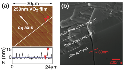
Figure 2(a) is an AFM phase image of the film, showing periodic buckling and cracking of the film parallel to cR, with inter-crack spacings on the order of . The depth profile reveals nanosized ridges, high, near the cracks. The SEM image in Fig. 2(b) confirms the thickness of the film. It shows that the cracks’ depth matches the film thickness and it gives an estimate of about for their width. Such nanocracks were not detected by the AFM due to lack of tip sensitivity.
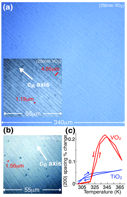
The optical images of the (Fig. 3(a)) and the (Fig. 3(b)) films confirm the period spacing of the cracks along cR. Also, the observed uniformity in the distribution of cracks is an indication that our films are strained in a highly homogeneous and oriented fashion. This crack distribution enables a comparison of our results with those of VO2 nanobeams, aligned along cR Cao2009 ; Zhang2009 ; Wu2006 ; Sohn2009 ; Jones2010 , although the dimensionality of our nanosheets gives access to the properties of strained VO2 along more than one axis. Such cracking uniformity was achieved by optimizing the growth conditions of the samples, in particular the growth temperature. In the case of our (100)R VO2 films the growth temperature was set to . Films grown at show cracking along different directions, which makes the characterization of the films along cR less straightforward. All subsequent analysis is analogous for both the and the thick films. Unless otherwise specified the results will refer to the thick sample.
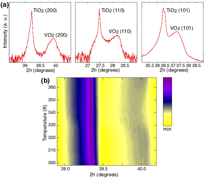
Detailed room temperature XRD of the VO2 film confirms the single crystal nature of the sample and yields the lattice parameters of the material (Fig. 4(a)). Comparing these values with those in the rutile phase of bulk VO2 McWhan1974 yields mismatches of along aR, along bR, and along cR, indicative of a compressive strain along aR and bR, as opposed to a tensile strain along cR. Such strain values along cR are comparable to those achieved in one-dimensional VO2 nanobeams Cao2009 . Bulk rutile TiO2 has larger lattice constants than bulk rutile VO2 along all directions so one would expect that both bR and cR would expand in (100)R VO2 films grown on a (100)R TiO2 substrate. However, our nanosheets show that the expansion along cR surpasses the substrate clamping effect due to the bR-axis, leading to a compressive strain in the abR-plane. This behavior is also observed in the thick film, with mismatches of along a, along b and along c.
Temperature dependent XRD results (Fig. 3(c)) show that a small aR-axis expansion, , occurs during the film’s structural transition. This transition occurs at a temperature , the same as in bulk, and shows the expected hysteric behavior. (From here on will refer to both bulk and film structural transition temperatures.) The aR-axis expansion in our strained sheet can be compared to that in bulk VO2, estimated as Andersson1956 ; Kucharczyk1979 , where bM is the equivalent of aR in the bulk monoclinic insulating structure. The order of magnitude difference between the lattice parameter variation in the film and that in bulk stems from the clamping effect of the rutile TiO2 substrate. This is consistent with the large strain observed in room temperature XRD, caused by the strong substrate clamping effect. The structural change exhibited at by our strained VO2 nanosheets is thus smaller than the change observed in bulk VO2. Since VO2 shares the TiO2 rutile structure at high temperatures, the reduced structural change is expected to have an impact mainly on the low temperature VO2 film’s structure. The temperature dependent (200)R plots from which the data in Fig. 3(c) were extracted are presented in Fig. 4(b). These raw data provide further support to our observation that the clamping effect due to the substrate is very strong, thereby preventing the development of significantly different structural phases in the strained VO2 film.
B. THz Time Domain Spectroscopy
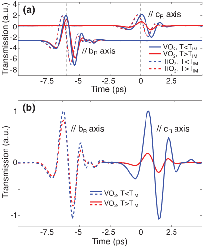
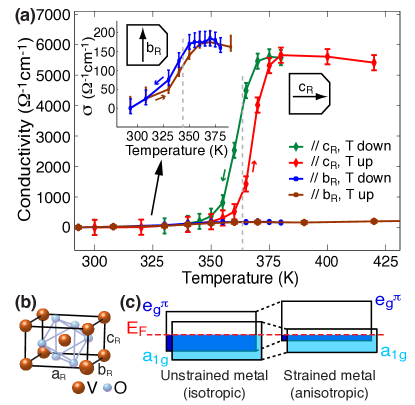
As shown in Fig. 1, upon increasing the temperature from the insulating to the metallic phase the THz peak transmission in the (100)R VO2 film drops by 70 along the cR-axis and by 15 along the bR-axis, and the THz peak transmission in the (100)R VO2 film drops by 85 along the cR-axis and by 15 along the bR-axis. Figure 1(b) shows the transmission anisotropy in our VO2 sample, normalized to its low temperature value along each axis (bR and cR). This representation highlights the dramatic difference between the low temperature transmission along bR and that along cR, thereby illustrating the potential of strained VO2 films as temperature tunable THz polarizing beamsplitters.
Figure 5(a) shows the temperature dependent far infrared conductivity, obtained from the transmission data, for the (100)R VO2 nanosheet. The conductivity along cR shows a clear transition from the insulating to the metallic state with a narrow hysteresis, which is indicative of the high quality of the film. In the metallic state the conductivity is , comparable to bulk single crystal values Ladd1969 . The MIT along cR occurs at a temperature . is significantly larger than both the structural transition temperature and the bulk MIT temperature, . Our VO2 films therefore exhibit, along cR, a temperature difference between the structural and the metal-insulator transition temperatures. The combination of the quasi three dimensionality of our nanosheets, which enables a direct measurement of the strain along the three crystal axes through XRD analysis, with the polarization sensitivity of THz spectroscopy is the key to identifying this distinction between the two transition temperatures.
The conductivity along bR also exhibits a transition (see inset of Fig. 5(a)), which occurs at . Along this direction we therefore observe that the structural and metal-insulator transition temperatures are the same, . However, the conductivity along bR reaches a high temperature value about 30 times smaller than the high temperature conductivity along cR. This strong conductivity anisotropy will be addressed later in the text.
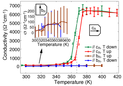
THz TDS results for the thick sample (Fig. 6) indicate that its transport properties are similar to that of the sample. In particular, the high temperature conductivity along cR remains as good as in bulk VO2 single crystals Ladd1969 while . The high temperature conductivity along bR is very low, , and the transition temperature can only be estimated at , consistent with and and in line with what is observed in the sample (Fig. 5(a)).
IV. DISCUSSION
Understanding the contribution of the V3d orbitals to the electronic properties is crucial in order to explain the large material anisotropy in Goodenough1971 . A splitting of the 5-fold degenerate 3d states occurs due to the octahedral coordination of the V atoms, resulting in a higher energy doubly degenerate level and a lower energy triply degenerate level. Trigonal distortion further splits the levels leading to an upshifted doubly degenerate state, responsible for conduction in the abR-plane, while downshifting a non-degenerate cR-oriented state (Fig. 5(b)). Recent cluster Dynamical Mean Field Theory (cDMFT) calculations Lazarovits2010 , which include the effect of a strain along cR, have demonstrated that a tensile strain along cR narrows the derived band and leads to a compressive strain in the abR-plane, which uplifts the band (Fig. 5(c)). In the Mott picture the energy increase of electrons reduces the screening of electrons residing in the band, thereby enhancing the effect of correlations (i.e. increasing the screened Hubbard U). This results in an increase of the insulating band gap which opens, below TMI, between the bonding and the anti-bonding levels, therefore leading to an increased along cR. Eyert2002 ; Zylbersztejn1975 .
The epitaxial strain in our film can be decomposed into a uniaxial tensile strain along cR and a uniaxial compressive strain along bR. Along cR, , in line with previous experimental results Muraoka2002 , while remains comparable to the best single crystal values Ladd1969 . These results agree with the Mott picture above, where the increased lattice spacing along cR further increases the ratio of Coulomb repulsion to the inter-atomic hopping integral, thereby destabilizing the metallic phase and increasing . The Peierls picture predicts a decrease in with tensile strain along cR, thus failing to describe our results along that axis Lazarovits2010 . Also contrary to the Peierls-driven MIT scenario along cR is the fact that the structural transition occurs at a temperature , lower than : in a Peierls picture both transitions would be expected to occur at the same temperature. In contrast to what happens along cR, the results along bR, where , are compatible with a Peierls-driven MIT scenario.
As mentioned above, our samples are cracked along cR. The occurrence of such cracks is common in VO2, in both bulk and strained samples Berglund1969 ; Nagashima2006 , and this has prevented accurate measurements of the DC conductivity in this material in the direction perpendicular to cR. Hindered quasiparticle motion along bR due to the presence of cR oriented cracks is the most likely explanation for the reduced value of in our films. However, a different scenario could arise in the THz range. Due to the small value of the far-infrared carrier mean free path ( Qazilbash2006 ) compared to DC, the long THz field should be able to couple to the material along bR despite the cracks along cR. According to this picture, the uniaxial compressive strain along bR would play a significant role in reducing , compared to , while keeping . Given the orbitals orientation, conductivity in the abR-plane is mediated by the orbitals whose energy is controlled by the overlap between O2p and V3d orbitals Eyert2002 . Low conductivity behavior in the compressed abR-plane for would then arise from the states being higher in energy than in the unstrained case, which reduces their overlap with the Fermi level (Fig. 5C). VO2 nanosheets that remain uncracked while maintaining a high level of strain along bR must be investigated in order to clarify the role of the orbitals on the high temperature value of , thereby also clarifying the nature of the MIT along that axis.
Our strained VO2 films on a TiO2 substrate have been shown to enable the separation of the far-infrared signal’s polarization components both in time and intensity. The temperature dependent THz conductivity of strained VO2 nanosheets (Figs. 5(a) and 6) shows that incident light polarized parallel to bR is transmitted through VO2 at both low and high temperatures, whereas incident light polarized parallel to cR is transmitted through VO2 at low temperatures but reflected at high temperatures. Our strained VO2 single crystal nanosheets can thus be thought of as temperature switchable far-infrared polarizing beamsplitters.
V. PHASE DIAGRAM
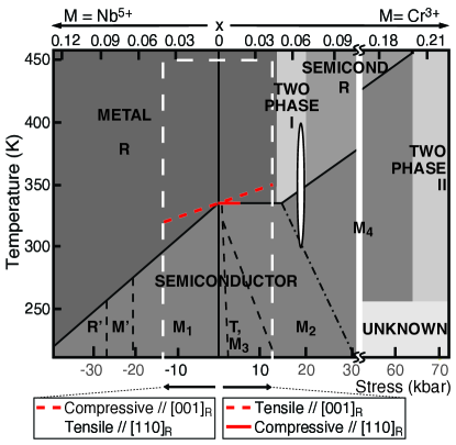
Finally, it is interesting to map the strain of our film onto the VO2 phase diagram in Fig. 7, constructed based on past studies of VO2 as a function of temperature, pressure Pouget1975 ; Cao2009 and doping Goodenough1973 ; Marezio1972 ; Pouget1976 ; Villeneuve1973 . In general, it is not trivial to map the effect of doping onto that of pressure. This was initiated by Pouget et al., who found a one-to-one correspondence between Cr-doping and the application of uniaxial stress along [110]R Pouget1975 ; Pouget1976 . Other doping experiments tend to indicate that doping ions with radii smaller than V4+ lead to an increase in whereas those with larger radii have the opposite effect MacChesney1969 . This is similar to what happens in V2O3, a canonical Mott insulator McWhan1969 .
Figure 7 compiles previous experimental results obtained on VO2 under different pressure Pouget1975 ; Cao2009 and doping Goodenough1973 ; Marezio1972 ; Pouget1976 ; Villeneuve1973 conditions. corresponds to atmospheric pressure. The application of hydrostatic pressure Neuman1964 ; Berglund1969Hyd ; Ladd1969 cannot be easily interpreted in terms of its influence on the conductivity nor on along individual axes of the crystalline structure, which corresponds to the main focus of our study. We therefore do not include hydrostatic pressure data in the phase diagram of Fig. 7. The dashed white lines delimit the region of the phase diagram where uniaxial pressure was applied along [001]R (up to ), both for compression () and tension (), and along [110]R (up to ), only for compression (). Within the rectangle, the dashed red line represents versus stress along cR, [001]R, while the solid red line represents versus stress in the abR-plane, [110]R. The dashed black lines separate different insulating phases within the low temperature monoclinic phase. The dash-doted line between phases M2 and M4 is a conjecture Goodenough1973 ; Villeneuve1973 . Note that apart from the dashed red line, relative to stress along [001]R, all the information in the diagram refers to stress along [110]R. The white oval indicates the phase space characteristic of our (100)R VO2 samples. The uniaxial stress on our films along [110]R has been estimated, respectively for the and the samples, to and , based on the measured and mismatch along (110)R, and on a Young modulus of Sepulveda2008 . These uniaxial stress values are higher than ever reported, to our knowledge, for uniaxial stress on VO2.
The dependence of on doping, studied in V1-xMxO2 compounds, can be approximately mapped onto its dependence on applied pressure. Reduction of V4+ is achieved using M = Nb, Mo, W, Ta, Re, Ir, F, Ti, Os, Ru, Tc, etc., with formal charges of +4, +5 or +6 Pouget1976 ; MacChesney1969 ; Goodenough1971 ; Beteille1998 ; Villeneuve1972 ; Piccirillo2007 ; Horlin1973 ; Holman2009 ; Nygren1969 ; Chae2008 ; Savborg1977 ; Bayard1975 ; Kristensen1968 ; Marinder1957 ; Gu2007 . The effect on is similar to that of negative (compressive) stress along [001]R, yielding . Oxidation of V4+ is achieved using M = Cr, Al, Fe, Ga, Ge, Sn, Mn, Co, etc., with formal charges of +3 or +4 Pouget1976 ; MacChesney1969 ; Goodenough1971 ; Beteille1998 ; Marezio1972 ; Villeneuve1973 ; Drillon1974 ; Kosuge1967 ; Pollert1976 ; Pintchovski1978 ; Kitahiro1967 ; Lee1996 . The effect on is similar to that of positive (tensile) stress along [001]R, yielding .
Our results, indicated by the white oval in the phase diagram of Fig. 7, are comparable to those of Everhart et al., where an anisotropy of about two orders of magnitude is observed in the metallic phase of bulk VO2 single crystals doped with iron at Everhart1968 . Our estimate of the stress puts our samples in a region of the phase diagram where TMI increases with stress, and where a two phase behavior is expected above TMI. This is consistent with our observation of both insulating () and metallic () values of in the same rutile structure, above . The independence of the conductivity behavior from the structural phase has been reported before Kim2006 ; Qazilbash2011 ; Arcangeletti2007 , though relative to monoclinic structures. As for the low temperature structure, M4 or rutile seem to be the most likely candidates, although we cannot distinguish between the two. M1, M2 and M3/T are all structurally too far from rutile Marezio1972 ; Goodenough1973 ; Jones2010 to lead to the results shown in Fig. 3C, and they are located in different regions of the phase diagram, as seen in Fig. 7. These observations, along with the strong conductivity anisotropy exhibited by our strained nanosheets, are indicative of a more complex behavior of VO2, beyond the currently accepted doping and strain dependence of its structural and transport properties (Fig. 7).
Coming back to the conductivity measured in our strained nanosheets, it is important to point out that its anisotropy is unexpectedly large compared to previous experimental observations and theoretical calculations on VO2 samples Lu2008 ; Barker1966 ; Everhart1968 ; Bongers1965 ; Kosuge1967 . The anisotropy in the DC conductivity, or , in undoped VO2 samples is generally 1 for but can take many different values for (Table 1). Differences in sample quality and stoichiometry as well as in conductivity measurement techniques surely affect the results, but variations in geometry and internal strain / cracking are likely to also have an effect on the anisotropy of metallic VO2.
Tables 1 and 2 present a complete and up to date review, to our knowledge, of the experimental and theoretical data on conductivity anisotropy in VO2, including the effect of externally applied stress. Table 1 includes the results for the conductivity anisotropy, above and below TMI, when no external stress is applied Bongers1965 ; Barker1966 ; Kosuge1967 ; Everhart1968 ; Verleur1968 ; Continenza1999 ; Mossanek2007 ; Lysenko2007 ; Lu2008 ; Tomczak2009 . Table 2 presents several results for the strain induced variation of TMI and of the conductivity in VO2, for situations where hydrostatic or uniaxial pressure is applied to the samples Minomura1964 ; Neuman1964 ; Berglund1969Hyd ; Ladd1969 ; Pouget1975 ; Gregg1997 ; Muraoka2002 ; Arcangeletti2007 ; Lu2008 ; Sakai2008 ; Cao2009 .
As seen in tables 1 and 2, in most situations where uniaxial pressure is applied the conductivity is measured along cR, the only axis along which it is well defined due to geometry constraints of the samples or to cracking. Few studies determine the conductivity along aR or bR as a function of applied pressure. In general, it is agreed that (i) an applied uniaxial compressive (tensile) stress along the cR-axis leads to an increased (decreased) conductivity at ; (ii) an applied uniaxial compressive (tensile) stress along the cR-axis leads to a decreased (increased) (the axis along which is measured is not always specified); (iii) a small uniaxial stress applied along the [110]R direction has no significant effect on the conductivity nor along cR but it promotes a phase transition between different monoclinic structures (M1, M2, T/M3, M4), in the insulating phase Pouget1975 ; Marezio1972 ; Goodenough1973 . Further experiments are needed in order to systematically measure the conductivity along aR or bR under (i) an applied uniaxial stress along aR or bR; (ii) an applied uniaxial stress along cR; (iii) hydrostatic pressure. Also, clear criteria for distinguishing from would be extremely valuable to help draw a more accurate and complete phase diagram, in line with what has been attempted in previous studies Kim2006 ; Qazilbash2011 ; Arcangeletti2007 . The highly oriented strain across a quasi three dimensional structure, achieved in epitaxially grown VO2 nanosheets, offers an extraordinary versatility and potential for investigation of these issues.
Theoretically, several pictures have been suggested to explain the anisotropy in (unstrained) VO2: (1) a two band model description of 3d electrons, within the framework of the Goodenough model, predicts a non conducting abR-plane for , any residual conductivity in that plane being due to the overlap of O2p and V3d orbitals Goodenough1971 ; Eyert2002 ; (2) LDA calculations by Allen’s group predict the structural distortion to be the main force driving the MIT in VO2, following a simple Peierls picture Wentzcovitch1994 ; (3) a three-band Hubbard model, suggested by Tanaka et al., predicts a one dimensional conducting phase along cR for and an isotropically conducting phase for Tanaka2003 ; (4) LDA+cDMFT calculations by Biermann et al. suggest that electron correlations within the e levels are weaker than those along the a1g ones Biermann2005 ; (5) subsequent LDA+cDMFT calculations by Kotliar’s group, which include a moderate degree of uniaxial strain, suggest that electronic correlations are the main driving force in the MIT, and that the rutile phase itself should be able to support both metallic and insulating electronic behavior Lazarovits2010 ; (6) Liebsch et al. compared the LDA+U, DMFT and GW methods and found that none of them provides a full description of VO2, namely of the development of the insulating gap below TMI Liebsch2005 . Nonetheless, most of the calculations based on unstrained VO2 samples agree that (i) a1g and e states can be regarded as nearly independent; (ii) the conductivity is expected to be of predominantly a1g behavior for and nearly isotropic for ; (iii) electron correlations should be included in the model, mainly in the cR oriented a1g levels. Our results agree with (i) and (iii), while strain induced cracking prevents the accurate description of the effect mentioned in (ii). Further theoretical investigations should take into account not only strain Lazarovits2010 but also the oxygen degrees of freedom, in order to provide a more accurate description of the O2p and V3d orbitals overlap, most relevant for describing the conductivity in the abR-plane, and of the subsequent cracking along cR. Such estimates would be adequate for a quantitative, rather than merely qualitative, comparison with our experimental data.
VI. CONCLUSION
In summary, we have observed a large anisotropy of the properties of strained and thick VO2 nanosheets. The increased value of compared to is a clear signature of a Mott- rather than Peierls-driven MIT along cR. An orbital tuning picture is proposed to explain the reduced value of the high temperature , although a crack induced conductivity decrease cannot be conclusively ruled out. Additional experiments are needed in order to clarify the mechanism of the phase transition in strained VO2, mainly in the direction perpendicular to cR. This would allow the development of a more comprehensive phase diagram for this material. In general, epitaxial strain engineering is a powerful tool which has the potential to enable careful tuning of the metal-insulator transition in numerous other correlated electron materials, thereby providing a viable route towards technologically relevant multifunctionality and increased understanding of the microscopic origin of the MIT.
ACKNOWLEDGMENTS
We thank Kebin Fan and Wei Zhang for SEM sample characterization. We acknowledge support from DOE - Basic Energy Sciences under Grant No. DE-FG02-09ER46643 (E.A., M.L., R.D.A.). E. Abreu acknowledges support from Fundação para a Ciência e a Tecnologia, Portugal, through a doctoral degree fellowship (SFRH/ BD/ 47847/ 2008).
References
- (1) L. A. Ladd and W. Paul, Solid State Communications 7, 425 (1969)
- (2) G. Andersson, Acta Chemica Scandinavica 10, 623 (1956)
- (3) S. Biermann, A. Poteryaev, A. Lichtenstein, and A. Georges, Physical Review Letters 94, 026404 (Jan. 2005), ISSN 0031-9007, http://link.aps.org/doi/10.1103/PhysRevLett.94.026404
- (4) B. Lazarovits, K. Kim, K. Haule, and G. Kotliar, Physical Review B 81, 115117 (Mar. 2010), ISSN 1098-0121, http://link.aps.org/doi/10.1103/PhysRevB.81.115117
- (5) H.-T. Kim, Y. W. Lee, B.-J. Kim, B.-G. Chae, S. J. Yun, K.-Y. Kang, K.-J. Han, K.-J. Yee, and Y.-S. Lim, Physical Review Letters 97, 266401 (Dec. 2006), ISSN 0031-9007, http://link.aps.org/doi/10.1103/PhysRevLett.97.266401
- (6) M. Qazilbash, A. Tripathi, A. Schafgans, B.-J. Kim, H.-T. Kim, Z. Cai, M. Holt, J. Maser, F. Keilmann, O. Shpyrko, and D. Basov, Physical Review B 83, 165108 (Apr. 2011), ISSN 1098-0121, http://link.aps.org/doi/10.1103/PhysRevB.83.165108
- (7) E. Arcangeletti, L. Baldassarre, D. Di Castro, S. Lupi, L. Malavasi, C. Marini, A. Perucchi, and P. Postorino, Physical Review Letters 98, 196406 (May 2007), ISSN 0031-9007, http://link.aps.org/doi/10.1103/PhysRevLett.98.196406
- (8) H.-T. Kim, B.-G. Chae, D.-H. Youn, G. Kim, K.-Y. Kang, S.-J. Lee, K. Kim, and Y.-S. Lim, Applied Physics Letters 86, 242101 (2005), ISSN 00036951, http://link.aip.org/link/APPLAB/v86/i24/p242101/s1&Agg=doi
- (9) T. Driscoll, H.-T. Kim, B.-G. Chae, B.-J. Kim, Y.-W. Lee, N. M. Jokerst, S. Palit, D. R. Smith, M. Di Ventra, and D. N. Basov, Science 325, 1518 (Sep. 2009), ISSN 1095-9203, http://www.ncbi.nlm.nih.gov/pubmed/19696311
- (10) D. Hilton, R. Prasankumar, S. Fourmaux, A. Cavalleri, D. Brassard, M. El Khakani, J. Kieffer, A. Taylor, and R. Averitt, Physical Review Letters 99, 226401 (Nov. 2007), ISSN 0031-9007, http://link.aps.org/doi/10.1103/PhysRevLett.99.226401
- (11) Y. Muraoka, Y. Ueda, and Z. Hiroi, Journal of Physics and Chemistry of Solids 63, 965 (Aug. 2002), ISSN 00223697, http://linkinghub.elsevier.com/retrieve/pii/S0022369702000987
- (12) J. Lu, K. G. West, and S. a. Wolf, Applied Physics Letters 93, 262107 (2008), ISSN 00036951, http://link.aip.org/link/APPLAB/v93/i26/p262107/s1&Agg=doi
- (13) S. Zhang, J. Y. Chou, and L. J. Lauhon, Nano Letters 9, 4527 (Dec. 2009), ISSN 1530-6992, http://www.ncbi.nlm.nih.gov/pubmed/19902918
- (14) K. G. West, J. Lu, J. Yu, D. Kirkwood, W. Chen, Y. Pei, J. Claassen, and S. a. Wolf, Journal of Vacuum Science & Technology A 26, 133 (2008), ISSN 07342101, http://link.aip.org/link/JVTAD6/v26/i1/p133/s1&Agg=doi
- (15) P. Jepsen, D. Cooke, and M. Koch, Laser & Photonics Reviews 5, 124 (Jan. 2011), ISSN 18638880, http://doi.wiley.com/10.1002/lpor.201000011
- (16) C. Jördens, M. Scheller, M. Wichmann, M. Mikulics, K. Wiesauer, and M. Koch, Applied optics 48, 2037 (Apr. 2009), ISSN 1539-4522, http://www.ncbi.nlm.nih.gov/pubmed/19363540
- (17) J. Cao, E. Ertekin, V. Srinivasan, W. Fan, S. Huang, H. Zheng, J. W. L. Yim, D. R. Khanal, D. F. Ogletree, J. C. Grossman, and J. Wu, Nature Nanotechnology 4, 732 (Sep. 2009), ISSN 1748-3387, http://www.nature.com/doifinder/10.1038/nnano.2009.266
- (18) J. Wu, Q. Gu, B. S. Guiton, N. P. de Leon, L. Ouyang, and H. Park, Nano Letters 6, 2313 (Oct. 2006), ISSN 1530-6984, http://www.ncbi.nlm.nih.gov/pubmed/17034103
- (19) J. I. Sohn, H. J. Joo, D. Ahn, H. H. Lee, A. E. Porter, K. Kim, D. J. Kang, and M. E. Welland, Nano Letters 9, 3392 (Oct. 2009), ISSN 1530-6992, http://www.ncbi.nlm.nih.gov/pubmed/19785429
- (20) A. C. Jones, S. Berweger, J. Wei, D. Cobden, and M. B. Raschke, Nano Letters 10, 1574 (May 2010), ISSN 1530-6992, http://www.ncbi.nlm.nih.gov/pubmed/20377237
- (21) D. B. McWhan, M. Marezio, J. P. Remeika, and P. D. Dernier, Physical Review B 10, 490 (1974)
- (22) D. Kucharczyk and T. Niklewski, Journal of Applied Crystallography 12, 370 (1979)
- (23) J. Goodenough, Journal of Solid State Chemistry 3, 490 (Nov. 1971), ISSN 00224596, http://linkinghub.elsevier.com/retrieve/pii/0022459671900910
- (24) V. Eyert, Annalen der Physik (Leipzig) 11, 650 (Oct. 2002), ISSN 00033804, http://doi.wiley.com/10.1002/1521-3889(200210)11:9<650::AID-ANDP650>3.0%.CO;2-K
- (25) A. Zylbersztejn and M. N. F., Physical Review B 11, 4383 (1975)
- (26) C. N. Berglund and H. J. Guggenheim, Physical Review 185, 1022 (1969)
- (27) K. Nagashima, T. Yanagida, H. Tanaka, and T. Kawai, Physical Review B 74, 172106 (Nov. 2006), ISSN 1098-0121, http://link.aps.org/doi/10.1103/PhysRevB.74.172106
- (28) M. Qazilbash, K. Burch, D. Whisler, D. Shrekenhamer, B. Chae, H. Kim, and D. Basov, Physical Review B 74, 205118 (Nov. 2006), ISSN 1098-0121, http://link.aps.org/doi/10.1103/PhysRevB.74.205118
- (29) J. P. Pouget, H. Launois, J. P. D’Haenens, P. Merenda, and T. M. Rice, Physical Review Letters 35, 873 (1975)
- (30) J. B. Goodenough and H. Y.-P. Hong, Physical Review B 8, 1323 (1973)
- (31) M. Marezio, D. B. McWhan, J. P. Remeika, and P. D. Dernier, Physical Review B 5, 2541 (1972)
- (32) J. P. Pouget and H. Launois, Journal de Physique Colloques 37, C4 (1976)
- (33) P. Villeneuve, G., Drillon, M., Hagenmuller, Materials Research Bulletin 8, 1111 (1973)
- (34) J. Macchesney and H. Guggenheim, Journal of Physics and Chemistry of Solids 30, 225 (Feb. 1969), ISSN 00223697, http://linkinghub.elsevier.com/retrieve/pii/0022369769903035
- (35) D. B. McWhan, T. M. Rice, and J. P. Remeika, Physical Review Letters 23, 1384 (1969)
- (36) H. J. Barker, A. S., Verleur, H. W., Guggenheim, Physical Review Letters 17, 1286 (1966)
- (37) J. B. Everhart, C. R., MacChesney, Journal of Applied Physics 39, 2872 (1968)
- (38) P. F. Bongers, Solid State Communications 3, 275 (1965)
- (39) K. Kosuge, Journal of the Physical Society of Japan 22, 551 (1967)
- (40) C. H. Neuman, A. W. Lawson, and R. F. Brown, The Journal of Chemical Physics 41, 1591 (1964)
- (41) C. N. Berglund and A. Jayamaran, Physical Review 185, 1034 (1969)
- (42) N. Sepúlveda, A. Rúa, R. Cabrera, and F. Fernández, Applied Physics Letters 92, 191913 (2008), ISSN 00036951, http://link.aip.org/link/APPLAB/v92/i19/p191913/s1&Agg=doi
- (43) F. Béteille and J. Livage, Journal of Sol-Gel Science and Technology 13, 915 (1998)
- (44) G. Villeneuve, A. Bordet, A. Casalot, J. Pouget, H. Launois, and P. Lederer, Journal of Physics and Chemistry of Solids 33, 1953 (Jul. 1972), ISSN 00381098, http://linkinghub.elsevier.com/retrieve/pii/003810987291191X
- (45) C. Piccirillo, R. Binions, and I. P. Parkin, European Journal of Inorganic Chemistry 2007, 4050 (Sep. 2007), ISSN 14341948, http://doi.wiley.com/10.1002/ejic.200700284
- (46) M. Hörlin, T., Niklewski, T., Nygren, Materials Research Bulletin 8, 179 (1973)
- (47) K. Holman, T. McQueen, A. Williams, T. Klimczuk, P. Stephens, H. Zandbergen, Q. Xu, F. Ronning, and R. Cava, Physical Review B 79, 245114 (Jun. 2009), ISSN 1098-0121, http://link.aps.org/doi/10.1103/PhysRevB.79.245114
- (48) M. Nygren, M., Israelsson, Materials Research Bulletin 4, 881 (1969)
- (49) B. G. Chae, H. T. Kim, and S. J. Yun, Electrochemical and Solid-State Letters 11, D53 (2008), ISSN 10990062, http://link.aip.org/link/ESLEF6/v11/i6/pD53/s1&Agg=doi
- (50) O. Sävborg and M. Nygren, Physica Status Solidi (a) 43, 645 (Oct. 1977), ISSN 00318965, http://doi.wiley.com/10.1002/pssa.2210430236
- (51) M. Bayard, Journal of Solid State Chemistry 12, 41 (Jan. 1975), ISSN 00224596, http://linkinghub.elsevier.com/retrieve/pii/0022459675901760
- (52) I. K. Kristensen, Journal of Applied Physics 39, 5341 (1968)
- (53) B.-O. Marinder and A. Magnéli, Acta Chemica Scandinavica 11, 1635 (1957)
- (54) Q. Gu, A. Falk, J. Wu, L. Ouyang, and H. Park, Nano Letters 7, 363 (Mar. 2007), ISSN 1530-6984, http://www.ncbi.nlm.nih.gov/pubmed/17256915
- (55) M. Drillon and G. Villeneuve, Materials Research Bulletin 9, 1199 (1974)
- (56) E. Pollert, G. Villeneuve, F. Ménil, and P. Hagenmuller, Materials Research Bulletin 11, 159 (1976)
- (57) F. Pintchovski, W. S. Glaunsinger, and A. Navrotsky, Journal of the Physics and Chemistry of Solids 39, 941 (1978)
- (58) I. Kitahiro and A. Watanabe, Japanese Journal of Applied Physics 6, 1023 (1967)
- (59) M.-H. Lee, M.-G. Kim, and H.-K. Song, Thin Solid Films 290-291, 30 (1996)
- (60) H. W. Verleur, A. S. Barker, and C. N. Berglund, Physical Review 172, 788 (1968)
- (61) a. Continenza, S. Massidda, and M. Posternak, Physical Review B 60, 15699 (Dec. 1999), ISSN 0163-1829, http://link.aps.org/doi/10.1103/PhysRevB.60.15699
- (62) R. J. O. Mossanek and M. Abbate, Journal of Physics: Condensed Matter 19, 346225 (Aug. 2007), ISSN 0953-8984, http://stacks.iop.org/0953-8984/19/i=34/a=346225?key=crossref.097329a85%05cf348ca29f0117d3a15db
- (63) S. Lysenko, V. Vikhnin, F. Fernandez, A. Rua, and H. Liu, Physical Review B 75, 075109 (Feb. 2007), ISSN 1098-0121, http://link.aps.org/doi/10.1103/PhysRevB.75.075109
- (64) J. Tomczak and S. Biermann, Physical Review B 80, 1 (Aug. 2009), ISSN 1098-0121, http://link.aps.org/doi/10.1103/PhysRevB.80.085117
- (65) S. Minomura and H. Hagasaki, Journal of the Physical Society of Japan 19, 131 (1964)
- (66) J. M. Gregg and R. M. Bowman, Applied Physics Letters 71, 3649 (1997), ISSN 00036951, http://link.aip.org/link/APPLAB/v71/i25/p3649/s1&Agg=doi
- (67) J. Sakai, Journal of Applied Physics 104, 073703 (2008), ISSN 00218979, http://link.aip.org/link/JAPIAU/v104/i7/p073703/s1&Agg=doi
- (68) R. M. Wentzcovitch, W. W. Schulz, and P. B. Allen, Physical Review Letters 72, 3389 (1994)
- (69) A. Tanaka, Journal of the Physics Society Japan 72, 2433 (Oct. 2003), ISSN 0031-9015, http://jpsj.ipap.jp/link?JPSJ/72/2433/
- (70) a. Liebsch, H. Ishida, and G. Bihlmayer, Physical Review B 71, 085109 (Feb. 2005), ISSN 1098-0121, http://link.aps.org/doi/10.1103/PhysRevB.71.085109
| publication | sample type | method | anisotropy | anisotropy |
| below | above | |||
| Bongers et al. | bulk single crystal | two-probe | 2 | 2.5 |
| (1965) | (needle along cR, | |||
| 6x0.3x0.15) | ||||
| Barker et al. | bulk polycrystal | Hall voltage | 0.7-0.8 | 1.1-2 |
| (1966) | (well defined cR) | |||
| Kosuge et al. | bulk single crystal | two-probe | 1.14 | 0.58 |
| (1967) | ||||
| Koide et al. | single crystal film | two probe | 2 | 0.001-0.1 |
| (1967) | on rutile substrate | |||
| bulk single crystal | two-probe | 0.33 | ||
| (needle along cR, | ||||
| 3x0.8x0.07) | ||||
| Everhart et al. | bulk single crystal | four-probe | 2-10 | 7.5 |
| (1968) | (4-7x1-4x1-4) | |||
| Verleur et al. | bulk single crystal | reflectivity | 0.28-1.4 | 0.79-2 |
| (1968) | (0.25-) | |||
| Continenza et al. | (calculations) | model GW | 3-6.7 | N/A |
| (1999) | (0-10) | |||
| Mossanek et al. | (calculations) | LDA (0-12) | 0.6- | 0.7-3.3 |
| (2007) | ||||
| Lysenko et al. | 30 film on | optical (400) | 1.05 | 1 |
| (2007) | (012) Al2O3 | diffraction | ||
| Lu et al. | 40 film on | star-shaped | 5.14 | 1 |
| (2008) | (011)R TiO2 | electrodes | ||
| Tomczak et al. | (calculations) | LDA+CDMFT | 0.73-1.67 | 0.96-1.14 |
| (2009) | (0-5) | |||
| our results | 100 film on | THz TDS | N/A | 30 |
| (2010) | (100)R TiO2 | (far infrared) |
| publication | sample | applied | conductivity | conductivity | ||
| type | pressure | vs. pressure | along… | [K/kbar] | along… | |
| Minomura et al. | bulk | uniaxial | not specified | not specified | -0.46 | not specified |
| (1964) | (Drickamer cell, | |||||
| up to 160kbar) | ||||||
| Neuman et al. | single crystal | hydrostatic | increases | not specified | no significant | not specified |
| (1964) | (up to 6kbar) | below | change | |||
| powder | hydrostatic | increases | not specified | no significant | not specified | |
| (up to 6kbar) | change | |||||
| Berglund et al. | bulk single crystal | hydrostatic | increases; | cR | 0.082 | cR |
| (1969) | (0.25x0.25x0.2in, | (up to 44kbar) | saturates above | |||
| crack along cR) | , at 15-20kbar | |||||
| Ladd et al. | bulk single crystal | hydrostatic | increases | cR | 0.06 | cR |
| (1969) | (10x1x1mm) | (up to 8kbar) | (up to 30kbar, | |||
| at Troom) | ||||||
| along aR or bR | N/A | cR | no significant | cR | ||
| change | ||||||
| along cR | increases | cR | -1.2 | cR | ||
| (up to 0.5kbar) | below | |||||
| Pouget et al. | bulk single crystal | along [110]R | no significant | cR | no significant | cR |
| (1975) | (0.5mm2x2mm, | (up to 1.2kbar) | change | change | ||
| 3mm2x4mm) | ||||||
| Gregg et al. | thin films on | in-plane | increases | not specified | N/A | N/A |
| (1997) | Al2O3(012) | (3-point bend) | below | |||
| Muraoka et al. | 10-15nm thick | along cR | increases | aR or bR | aR or bR | |
| (2002) | single crystal thin | (epitaxial: | for [001]R; | for [001]R; | ||
| films on (001)R | -0.3 for (001)R, | not specified | not specified | |||
| and (110)R TiO2 | 1.2 for (110)R) | for [110]R | for [110]R | |||
| Arcangeletti et al. | single crystal | uniaxial | increases below | not specified | N/A | N/A |
| (2007) | (5m thick slab) | (diamond a. c., | ||||
| up to 140kbar) | (750-6000cm-1) | |||||
| Lu et al. | single crystal | in-plane | N/A | aR or bR | aR or bR | |
| (2008) | thin film on | (epitaxial: | ||||
| (011)R TiO2 | -1.2//[011]R, | |||||
| -0.4//[001]R) | ||||||
| Sakai | polycrystalline thin | in-plane | increases | not specified | not specified | |
| (2008) | film on metallic Ti | (point contact, | ||||
| (aR in plane) | up to 255kbar | |||||
| Cao et al. | single crystal | along cR | increases | cR | -2 | cR |
| (2009) | (0.5-2x0.5-2x100 | (3-point bend, | (optical) | |||
| nm, along cR) | up to 12kbar) | |||||
| our results | single crystal | in-plane | no significant | cR | cR | |
| (2010) | thin film on | (epitaxial: | change (far IR)) | |||
| (100)R TiO2 | //[001]R, | decreases above | bR | no significant | bR | |
| //[010]R) | (far IR) | change |