abbr
Chapter 7: Computational design of chemical nanosensors: Transition metal doped single-walled carbon nanotubes
Summary
We present a general approach to the computational design of nanostructured chemical sensors. The scheme is based on identification and calculation of microscopic descriptors (design parameters) which are used as input to a thermodynamic model to obtain the relevant macroscopic properties. In particular, we consider the functionalization of a (6,6) metallic armchair single-walled carbon nanotube (SWNT) by nine different transition metal (TM) atoms occupying three types of vacancies. For six gas molecules (N2, O2, H2O, CO, NH3, H2S) we calculate the binding energy and change in conductance due to adsorption on each of the 27 TM sites. For a given type of TM functionalization, this allows us to obtain the equilibrium coverage and change in conductance as a function of the partial pressure of the “target” molecule in a background of atmospheric air. Specifically, we show how Ni and Cu doped metallic (6,6) SWNTs may work as effective multifunctional sensors for both CO and NH3. In this way, the scheme presented allows one to obtain macroscopic device characteristics and performance data for nanoscale (in this case SWNT) based devices.
1 Introduction
Detecting specific chemical species at small concentrations is of fundamental importance for many industrial and scientific processes, medical applications, and environmental monitoring. Nanostructured materials are ideally suited for sensor applications because of their large surface to volume ratio, making them sensitive to the adsorption of individual molecules.
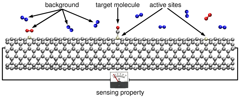
At a general level, any nanosensing system consists of the following four main components:
-
1.
a “target molecule” to be detected,
-
2.
an “active site” where the target molecule may adsorb on the sensor,
-
3.
a “sensing property” which changes upon adsorption of the target molecule,
-
4.
a “background” of adsorbing molecules which make up the background signal.
The active site must be designed so that adsorption of the target molecule in the presence of the background is sufficient to change the sensing property. These four main components of a chemical sensor are shown schematically in Figure 1, for the case of a transition metal (TM) doped (6,6) metallic armchair single-walled carbon nanotube (SWNT) measuring CO under atmospheric conditions.
Performing a screening study of possible SWNT dopings experimentally would be quite demanding, especially considering the great variety of potential active sites and target molecules one may wish to detect. On the other hand, computational screening studies based on density functional theory (DFT) calculations have recently been shown to be quite effective at shortening lists of potential candidates, which may then be studied experimentally.
The energetics obtained from DFT calculations using a generalized gradient approximation (GGA) for the exchange and correlation (xc)-functional are sufficiently accurate to provide a quantitative description of the stability of an active site, and the adsorption energies for both the target molecule and the background. From this data we may use kinetic modeling to estimate the equilibrium coverage of active sites by target molecules as a function of their pressure in the presence of the background. This allows us to quickly screen a wide variety of active sites, and rule out those which are completely oxidized in air, or too unstable at normal temperatures.
At the same time, changes in a nanosensor’s resistance are often used to detect adsorption of a target molecule. Trends in the resistance may be reasonably described using the non-equilibrium Green’s function (NEGF) methodology. In this way we may estimate the resistance per active site in the background, and hence determine the change in resistance of the active site as a function of target molecule concentration.
Using resistance as a sensing property has two main advantages. First, it is a non-intrusive measure, which should not significantly influence the adsorption of the target molecules. Second, small changes in the coverage of target molecules () often yield large changes in resistance (/site).
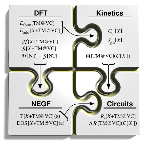
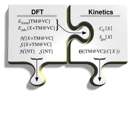
Overall, this procedure fits together like four “puzzle pieces”, DFT calculations, kinetic modeling, NEGF results and circuit theory, to calculate the average change in resistance as a function of a target molecule’s concentration . This methodology for modeling the chemical sensor is depicted schematically in Figure 2.
From DFT we obtain the formation energies of an active site (a 3 TM occupied vacancy (TM@VC)), the adsorption energies for species on the active site (+TM@VC), and the Hamiltonian and overlap matrices for the scattering region with adsorbed (+TM@VC) and the leads (a pristine (6,6) SWNT (NT)). The energetics from DFT are then inputted into a kinetic model for the active site in thermodynamic equilibrium with concentrations , and gas phase entropies , for each species taken from experiment [CRCHandbook]. From this we obtain the fractional coverage per active site (TM@VC) as a function of the target molecule’s concentration .
At the same time, the Hamiltonian and overlap matrices obtained from DFT are used within the NEGF methodology to obtain the density of states (DOS) and transmission probability T for each species on an active site (+TM@VC), as a function of energy . Finally the coverage and transmission probabilities are used within simple circuit theory to estimate the scattering resistance for species on an active site (+TM@VC), and hence derive the overall change in resistance for a particular active site (TM@VC) as a function of the target molecule’s concentration .
As a specific example of a chemical nanosensor we will consider the functionalization of a (6,6) SWNT by nine different TM atoms occupying three types of vacancies. For six gas molecules (N2, O2, H2O, CO, NH3, H2S) we calculate the binding energy and change in conductance due to adsorption on each of the 27 TM sites. For a given type of TM functionalization, this allows us to obtain the equilibrium coverage and change in conductance as a function of the partial pressure of the “target” molecule in a background of atmospheric air, as shown schematically in Figure 1, and described in [Juanma, Kirchberg].
We will begin by providing a brief overview of the properties of our candidate sensing materials, specifically 3 TM doped (6,6) SWNTs. We will then discuss in detail in separate sections the four components of our method for modeling nanosensors: DFT calculations, kinetic modeling, NEGF results, and circuit theory, along with the results obtained for the TM functionalized SWNTs.
2 TM Doped SWNTs as Nanosensors
To understand what a SWNT is [Iijima, Rubio1, Dresselhaus, Harris, cnt_review], one may imagine a sheet of graphene being rolled into a diminutive cylinder, which is very long ( cm) and narrow ( nm). The properties of the SWNT strongly depend on the way the graphene sheet is wrapped. To represent the way the graphene sheet is wrapped, two indices are used: (), where and are integers.
These two indices represent the number of unit cell vectors along the two principle directions in the crystal lattice of graphene, and . For a () SWNT, the circumference is then given by
| (1) |
The nanotube is metallic if , where is an integer, and semiconducting otherwise. If the tube is classified as an armchair SWNT, if the tube is called a zigzag SWNT, and otherwise the tube is known as chiral. Based on simple geometrical arguments, the diameter of a SWNT may be approximated using the relation
| (2) |
where Å. The strength, electronic structure, and high surface to volume ratio of SWNTs make them excellent materials for nanodevices.
SWNTs work remarkably well as detectors for small gas molecules, as demonstrated for both individual SWNTs [kong, collins, hierold, villalpando, rocha, Brahim] and SWNT networks [morgan, cnt_networks, Goldoni]. However, such sensitivity is most likely attributable to structural defects, vacancies, and junctions in the SWNT networks, as pristine SWNTs are inherently inert [cnt_networks]. Thus, to control a SWNT’s performance as a chemical sensor, one must control the location, type, and number of these structural defects. For this reason, the controlled doping and functionalization of SWNTs has become an area of increasing interest [PaolaRevModPhys], especially for substitutional doping with either N [PaolaNdopedCNTs] or B [PaolaBdopedCNTs].
Previous studies have shown that SWNTs are highly sensitive to most molecules upon functionalization [Fagan, Yagi, Yang, Chan, Yeung, Vo, Furst, Juanma, Krasheninnikov]. However, the difficulty is determining which specific molecules are present. In this study we show how changing the functionalization of the SWNT provides “another handle” for differentiating the SWNT’s response to different gases/molecules. In this way, one may not only detect that a molecule is present, but also differentiate which molecule is present.
Recent experimental advances now make the controlled doping of chirality selected SWNTs with metal atoms a possibility. Specifically, these include (1) photoluminesence, Raman and XAS techniques for measuring the fraction of various SWNT chiralities in an enriched sample [Kramberger07PRB, Ayala09PRB, DeBlauwe2010]; (2) the separation of SWNT samples by chirality using DNA wrapping [Zheng03NM, Zheng03S, TU09N, Li07JOTACS], chromatographic separation [Li07JOTACS, Fagan07JOTACS] and Density Gradient Ultracentrifugation (DGU) [Arnold06NN]; (3) SWNT resonators for measuring individual atoms of a metal vapor which adsorb on a SWNT [Bachtold, ZettlMassSensor]; and (4) aberration corrected low energy (50 keV) transmission electron microscopy (TEM) [Chuanhong]. The latter provides control over the formation of defects in situ by adjusting the energy of the electron beam above and below the threshold energy for defect formation at a specific location on the SWNT. These methods provide such a high level of control that it is now possible for experimentalists to take a specific SWNT chirality and dope the structure with individual metal atoms at a specified location.
At the same time, theorists are now able to embrace a “bottom up” approach to the design of nanosensors, harnessing the thermodynamics of self-assembly to find useful sensing devices in silico. With recent advances in both computational power and methodologies, theorists can now efficiently and accurately screen hundreds of candidate sensor designs using a combination of DFT for energetics of adsorption and stability, and NEGF methodologies for the electrical response [Juanma].
In this chapter, we have used nine of the ten TMs as candidates for substitutional doping of a (6,6) metallic armchair SWNT. The (6,6) SWNT was chosen as it is small enough to be efficiently calculated (24 atoms in the minimal unit cell, 144 TM@MV or 143 atoms for the TM@DVI, TM@DVII), and at the same time experimentally realizable [Dresselhaus]. We repeat the minimal unit cell 6 times to ensure convergence of the Hamiltonian to its bulk values at the borders of the cell. In other words, the unit cell is large enough that structural and electronic changes due to the TM in the vacancy are not felt at the unit cell boundary. The radius of the (6,6) SWNT is about 4.1 Å, while in experimental samples of chirality sorted tubes, the radius is typically around 7 Å.
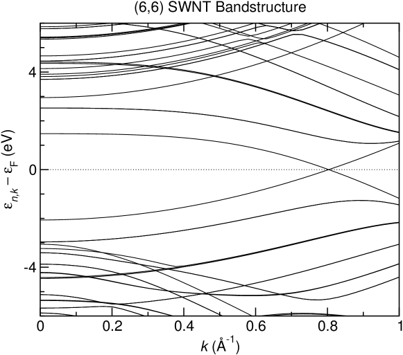
However, in the to 1 eV energy range of interest, for metallic tubes, the DOS is flat (2 eV-1), and has two open eigenchannels, so that T. This is clearly seen from the electronic band structure of the (6,6) SWNT, which is shown in Figure 3. In this way, the (6,6) SWNT results also provide a qualitative understanding of the response of larger metallic tubes. Further, for metallic armchair () SWNTs both the transmission T and DOS are completely flat near the Fermi level. This makes it much easier to differentiate the affect of the TM dopant, and the adsorbed molecule on the transmission and DOS.
The TM atoms have been chosen as candidate dopants for several reasons. First, the TM atoms are smaller for a given electronic configuration than the and TMs, and are expected to fit best in the structure of a SWNT, with the least strain. Even so, the TM atoms are typically pushed somewhat above the SWNT surface, due to both the strain on the graphene lattice, and the difference in atomic radii. These radii vary from the largest at 1.76 Å for Ti, to the smallest at 1.42 Å for Ni [Ashcroft]. These are all between 2 and 3 times the atomic radius of C of 0.67 Å. Also, the electronic properties of a TM dopant are mostly determined by the filling of the -band, and should be quite similar for the and counterparts of the TMs studied herein.
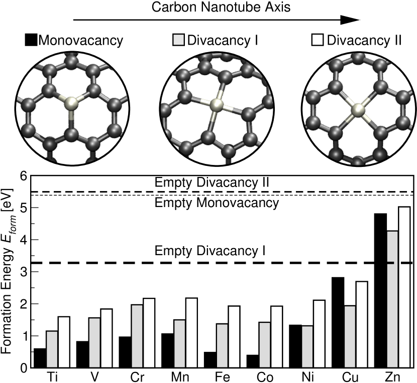
The monovacancy, divacancy I and divacancy II were considered here since these are the three most stable vacancies, as depicted schematically in Figure 4. Comparing divacancy I and divacancy II results shows the effect of strain on the electronic properties of the active site, since for the divacancy II the strain is evenly distributed over the four bonds, while for the divacancy I the strain is mostly on two of the four bonds, as seen in Figure 4. For the monovacancy, the TM dopant is three fold coordinated, while for the divacancies, the TM dopant is four-fold coordinated. This explains why in general we find molecules are more strongly bonded to TMs in a monovacancy compared to either of the divacancies.
For a strongly binding target molecule, such as CO, a divacancy provides the most suitable active site, as the site will not be completely saturated/covered, and a significant fraction of empty sites should always be present. On the other hand, for a weakly binding molecule, such as NH3, a monovacancy is more suitable, as there will then be a measurable change in coverage with molecule concentration.
3 Density Functional Theory
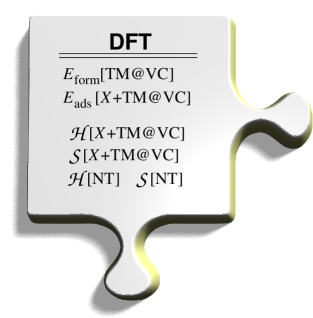
At its root, DFT is an exact reformulation of quantum mechanics in terms of the electron density [Kohn-Sham, Parr, DFTMarques, DFT2011]. In this way it is a quantum mechanical method for calculating the ground state energy for many-body systems. From this theory, we may calculate formation energies , adsorption energies , and a system’s Hamiltonian and overlap matrices, which form the first “puzzle piece” of our chemical nanosensor model, as shown in Figure 5.
The reason why DFT is used is that it simplifies a problem in terms of the many electron wave function into another problem, which is only in terms of the electron density . This is an important advantage because it reduces the coordinates from 3 to just 3 .
This is based on the Hohenberg Kohn theorem which states that for a given external potential the ground state energy is a unique functional of the electron density.
| (3) |
where
| (4) |
Here is the kinetic energy, describes the electron-electron interaction and is the external potential. However, an exact form for in terms of the density is unknown, so we approximate it by
| (5) |
Here is the exchange correlation potential that gives the correct electron-electron interaction . has corrections to the Coulomb potential in order to fulfill the Pauli exclusion principle, self interactions corrections, and electron-electron correlations.
The most common implementation of DFT uses the Kohn-Sham method. The procedure for this method is to assume a form for , and then solve the non-interacting Schrödinger equation
| (6) |
with the effective potential given by
| (7) |
This potential depends on the density
| (8) |
which in turn depends on the non-interacting Kohn-Sham wave functions , where is the number of electrons. We may thus obtain the wave functions and density by solving Eqns. (6), (7), and (8) in a self consistent manner. This Kohn-Sham self-consistency procedure is at the heart of DFT [Kohn-Sham].
In this work, all total energy calculations and structural optimizations have been performed within the real-space density functional theory (DFT) code gpaw [GPAW, GPAWRev] which is based on the projector augmented wave method (PAW) [Blochl]. This allows one to use a coarse grid, with “smoothed” pseudo-wave functions within the core, which describes the valence and conduction states quite well, to calculate the pseudo-density and pseudo-wave functions self-consistently. At the same time, it allows access to the full all-electron densities and wave functions, by projecting back onto the core wave functions on a finer grid. We find a grid spacing of 0.2 Å provides a quite accurate representation of both the density and wave functions. For the purposes of energetics of molecules and solids, the Perdew-Burke-Ernzerhof implementation of the GGA for the exchange correlation functional [PBE] works quite well. Spin polarization has been taken into account in all calculations. This is necessary, since TM atoms often have a magnetic moment, as do molecules in the atmosphere such as O2.
Pristine SWNTs are known to be chemically inert – a property closely related to their high stability. As a consequence, only radicals bind strong enough to the SWNT to notably affect its electrical properties [RevModPhys.79.677, hierold, Valentini2004356, zanolli:155447, Juanma]. To make SWNTs attractive for sensor applications thus requires some kind of functionalization, e.g. through doping or decoration of the SWNT sidewall [Fagan, Yagi, Yang, PaolaNdopedCNTs, Chan, Yeung, Vo, Furst, JuanmaPRL, PaolaBdopedCNTs, Krasheninnikov, PaolaRevModPhys]. Ideally, this type of functionalization could be used to control not only the reactivity of the SWNT but also the selectivity towards specific chemical species.
Metallic doping of a (6,6) SWNT has been modeled in a supercell containing six repeated minimal unit cells along the SWNT axis (dimensions: 15 Å15 Å14.622 Å). For this size of supercell a -point sampling of the Brillouin zone was found to be sufficient to obtain reasonably converged adsorption and formation energies. It should also be noted that for transport calculations within the NEGF method, it is implicitly assumed that the interaction between atoms near opposite ends of the unit cell are negligible, and any -point dependence along the transport direction is neglected.
We define the formation energy for creating a vacancy (VC) occupied by a TM atom using the relation
| (9) |
where [TM@VC] is the total energy of a TM atom occupying a vacancy in the nanotube, is the number of carbon atoms removed to form the vacancy, [C] is the energy per carbon atom in a pristine nanotube, and [TM+NT] is the total energy of the pristine nanotube with a physisorbed TM atom. The vacancies considered herein are the monovacancy and two divacancies shown in Figure 4. The energy required to form an empty vacancy is obtained from
| (10) |
where [VC] is the total energy of the nanotube with a vacancy of atoms.
The calculated formation energies for the TMs are shown in Figure 4. From the horizontal lines we see that both divacancies are more stable than the monovacancy. This may be attributed to the presence of a two-fold coordinated C atom in the monovacancy, while all C atoms remain three-fold coordinated in the divacancies. When a TM atom occupies a vacancy, the strongest bonding to the C atoms is through its orbitals [Griffith]. For this reason, Cu and Zn, which both have filled -bands, are rather unstable in the SWNT. For the remaining metals, adsorption in the monovacancies leads to quite stable structures. This is because the three-fold coordination of the C atoms and the SWNT’s hexagonal structure are recovered when the metal atom is inserted. On the other hand, metal adsorption in divacancies is slightly less stable because of the resulting pentagon defects, depicted in the upper panel in Figure 4. A similar behavior has been reported by Krasheninnikov et al. for TM atoms in graphene [Krasheninnikov].
| Ti | V | Cr | Mn | Fe | Co | Ni | Cu | Zn | |
|---|---|---|---|---|---|---|---|---|---|
| N2 | -0.61 | -0.76 | -0.57 | -0.70 | -0.77 | -0.60 | -0.49 | -0.34 | -0.51 |
| O2 | -3.16 | -3.39 | -2.61 | -2.57 | -2.17 | -1.88 | -2.00 | -1.02 | -0.90 |
| H2O | -1.09 | -1.08 | -0.97 | -0.89 | -0.84 | -0.64 | -0.54 | -0.52 | -0.62 |
| CO | -0.89 | -1.21 | -1.06 | -1.38 | -1.54 | -1.23 | -1.16 | -0.97 | -1.07 |
| NH3 | -1.39 | -1.46 | -1.35 | -1.32 | -1.31 | -1.03 | -0.94 | -0.89 | -1.12 |
| H2S | -0.78 | -0.88 | -0.77 | -0.78 | -0.88 | -0.58 | -0.69 | -0.63 | -0.67 |
| Ti | V | Cr | Mn | Fe | Co | Ni | Cu | Zn | |
|---|---|---|---|---|---|---|---|---|---|
| N2 | -0.58 | -0.65 | -0.65 | -0.38 | -0.46 | -0.63 | -0.15 | -0.01 | -0.01 |
| O2 | -2.72 | -3.41 | -2.74 | -1.92 | -1.67 | -1.42 | -0.61 | -0.06 | -0.12 |
| H2O | -1.21 | -1.19 | -0.79 | -0.49 | -0.51 | -0.33 | -0.19 | -0.05 | -0.25 |
| CO | -0.80 | -1.11 | -1.14 | -1.06 | -1.62 | -1.90 | -1.10 | -0.12 | -0.04 |
| NH3 | -1.51 | -1.58 | -1.11 | -0.89 | -0.91 | -0.75 | -0.40 | -0.20 | -0.53 |
| H2S | -0.87 | -0.78 | -2.13 | -0.50 | -0.64 | -0.59 | -0.31 | -0.04 | -0.17 |
| Ti | V | Cr | Mn | Fe | Co | Ni | Cu | Zn | |
|---|---|---|---|---|---|---|---|---|---|
| N2 | -0.50 | -0.62 | -0.41 | -0.38 | -0.60 | -0.39 | -0.07 | -0.02 | -0.11 |
| O2 | -2.27 | -2.64 | -2.35 | -2.17 | -1.48 | -1.31 | -0.53 | -0.09 | -0.18 |
| H2O | -1.15 | -1.20 | -0.74 | -0.64 | -0.49 | -0.55 | -0.16 | -0.05 | -0.17 |
| CO | -0.78 | -1.10 | -1.05 | -0.96 | -1.49 | -1.30 | -0.82 | 0.02 | 0.01 |
| NH3 | -1.45 | -1.47 | -1.14 | -1.09 | -0.99 | -0.68 | -0.23 | -0.13 | -0.42 |
| H2S | -0.80 | -0.83 | -0.62 | -0.62 | -0.56 | -0.50 | -0.10 | -0.01 | -0.10 |
The adsorption energies for N2, O2, H2O, CO, NH3, and H2S on the metallic site of the doped (6,6) SWNTs are shown in Tables 1, 2, and 3 for the TM occupied monovacancy, divacancy I, and divacancy II, respectively. The adsorption energy of a molecule is defined by
| (11) |
where [@TM@VC] is the total energy of molecule on a TM atom occupying a vacancy, and is the gas phase energy of the molecule.
From the adsorption energies shown in Tables 1, 2, and 3, we see that the earlier TMs tend to bind the adsorbates stronger than the late TMs. The latest metals in the series (Cu and Zn) bind adsorbates rather weakly in the divacancy structures. We also note that O2 binds significantly stronger than any of the three target molecules on Ti, V, Cr, and Mn (except for Cr in the divacancy I where H2S is found to spontaneously dissociate). Active sites containing these metals are therefore expected to be completely passivated if oxygen is present in the background. Further, we find H2O is rather weakly bound to most of the active sites. This ensures that these types of sensors are robust against changes in humidity.
4 Kinetic Modeling
The next “piece of the puzzle” for our chemical nanosensor model is the description of the coverage of our active sites by both target and background molecules using kinetic theory, as depicted in Figure 6.
| N2 | 74.96% | 1.988 meV/K | CO | 96.00 ppb | 2.050 meV/K |
| O2 | 20.11% | 2.128 meV/K | NH3 | 16.32 ppb | 2.000 meV/K |
| H2O | 4.00% | 1.959 meV/K | H2S | 0.96 ppb | 2.136 meV/K |
For a sensor containing hundreds, if not thousands of sites, the fractional coverage of sites is reasonably described by the fractional coverage in thermodynamic equilibrium at standard temperature and pressure in terms of the target molecule concentration. The adsorption reaction for a species on an empty active site * is then
| (12) |
Under equilibrium conditions, the rate of adsorption and desorption of species must be equal, so that
| (13) |
where is the rate of the adsorption reaction, is the forward rate constant, is the backward rate constant, is the atmospheric concentration, is the fraction of active sites which are empty, and is the fraction of active sites which are covered by species .
Using Eqn. (13) we may express the coverage of active sites by species in terms of the ratio of forward and backward rate constants and as
| (14) |
From kinetic theory, the ratio of rate constants may be obtained from the DFT adsorption energy as
| (15) |
where is Boltzmann’s constant, is the temperature, and is the gas phase entropy of species , as given in Table 4 [CRCHandbook].
Since Eqn. (13) is valid for all species in the set of background molecules , so long as our description of the background is sufficient, if we sum up all the fractional coverages for each species, and the fraction of sites which are empty, we should obtain unity. More specifically,
| (16) |
By simple repeated substitution of Eqn. (14) into Eqn. (16), we may express the fractional coverage of active sites by species in terms of the ratios of forward and backward rate constants, and concentrations in atmosphere as
| (17) |
| Ti | V | Cr | Mn | Fe | Co | Ni | Cu | Zn | |
|---|---|---|---|---|---|---|---|---|---|
| CO | -86 | -82 | -58 | -44 | -22 | -23 | -30 | -7 | +9 |
| NH3 | -66 | -72 | -46 | -46 | -31 | -30 | -38 | -2 | +12 |
| H2S | -91 | -96 | -70 | 68 | -49 | -49 | -50 | -14 | -7 |
| Ti | V | Cr | Mn | Fe | Co | Ni | Cu | Zn | |
|---|---|---|---|---|---|---|---|---|---|
| CO | -72 | -87 | -60 | -31 | +1 | +11 | +13 | -19 | -22 |
| NH3 | -44 | -68 | -60 | -37 | -27 | -28 | -10 | -15 | -2 |
| H2S | -71 | -101 | -22 | -54 | -38 | -36 | -15 | -23 | -18 |
| Ti | V | Cr | Mn | Fe | Co | Ni | Cu | Zn | |
|---|---|---|---|---|---|---|---|---|---|
| CO | -56 | -58 | -48 | -45 | +3 | +2 | +8 | -23 | -24 |
| NH3 | -29 | -43 | -44 | -39 | -16 | -21 | -14 | -18 | -7 |
| H2S | -56 | -69 | -66 | -59 | -34 | -30 | -21 | -22 | -21 |
To measure the “sensitivity” of an active site to the concentration of a target molecule, one should consider how the coverage of the active site by the target molecule changes with the concentration of the species in the atmosphere. It is only when there are changes in the active site’s coverage, that through the resulting changes in the sensing property, the nanosensor may be useful for a given species’ detection. Specifically, we find the logarithm of the change in coverage with concentration of the target molecule, i.e. the derivative
| (18) |
acts as a reasonable “descriptor” for an active site’s sensitivity to species .
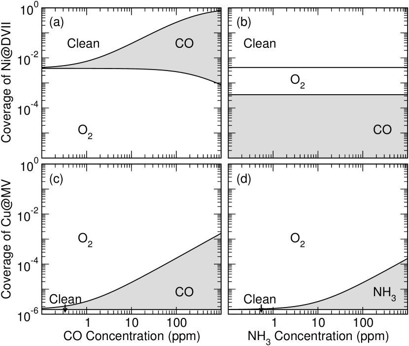
As shown in Table 5, in the monovacancy, only the relatively inert Cu and Zn active sites are at all sensitive to the target molecules, specifically for CO and NH3. This is due to the binding energy of O2, which is eV for all other TM atoms occupying monovacancies, but only eV for both Cu and Zn, as shown in Table 1. This leaves “clean” Cu@MV and Zn@MV active sites, where CO or NH3 may adsorb.
On the other hand, for both the divacancies shown in Tables 6 and 7 we find Fe, Co, and Ni are sensitive to CO. We attribute this to the similarity in binding energies for O2 and CO on these sites, which are between 0.5 and 1.6 eV, as shown in Tables 2 and 3. We again find Ti, V, Cr, and Mn are completely oxidized, as was the case in the monovacancy, making these sites inactive, while for Cu and Zn the binding energies of the target molecules are too weak for them to adsorb on these sites.
In Figure 7 we see the coverages of both Ni and Cu active sites as a function of CO and NH3 concentration. Clearly, both Cu and Ni active sites will be sensitive to the adsorption of CO. On the other hand, the coverage of the Cu active sites is sensitive to NH3 concentration, while Ni active sites are not. This suggests that by combining the response of Cu and Ni active sites, we may obtain a multifunctional sensor for both CO and NH3.
5 Non-Equilibrium Green’s Function Methodology
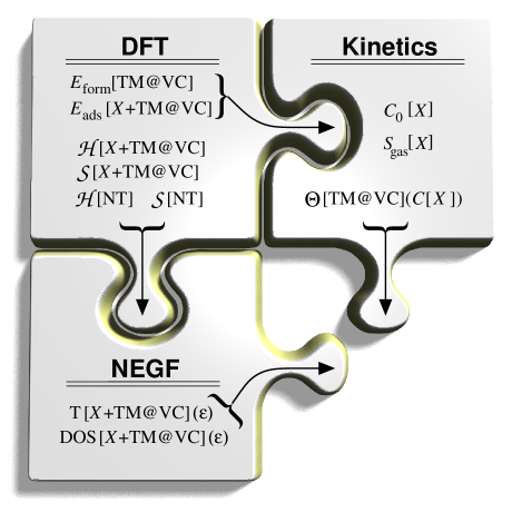
The third “puzzle piece” needed to model our chemical nanosensor is the description of the sensing property, specifically the change in resistance of the sensor using the NEGF method, as depicted in Figure 8. Although molecules may adsorb on the active sites, the sensing property of the SWNT resistance must change significantly for the sensor to be useful. In the following sections we show both the density of states (DOS) and transmission probability T() for an electron of a given energy to travel past an active site as calculated within the NEGF method.
Since the energy levels of a given molecule may be thought of as its electronic “finger print”, so long as there is sufficient binding between the molecule and active site, this “finger print” is evidenced in the DOS of the system. Furthermore, the peaks of the DOS due to the molecule tend to form Fano anti-resonances [Furst] in the transmission, as electrons are scattered off these states. In this way, any adsorbed molecule tends to leave its “finger print” in the transmission probability through an active site. For this reason, conductance/resistance is generally an effective sensing property.
The NEGF methodology [Datta] is based on the Green’s function, which is dependent on two space-time coordinates. The NEGF method can be applied to both extended and infinite systems and it can handle strong external fields without being perturbed. The approximations made in the NEGF method can be chosen in order to satisfy macroscopic conservation laws. An interesting feature of the NEGF method is that memory effects in transport that occur due to electron-electron interactions can be analyzed.
As depicted schematically in Figure 8, the NEGF method requires the Hamiltonian and overlap matrices for both the clean and doped SWNT structures. The NEGF calculation is then performed using as “leads” the clean SWNT Hamiltonian, with a “scattering region” defined by the doped SWNT Hamiltonian. Within this representation, the states which form the Hamiltonian must be in some way localized, so that the Hamiltonian of the scattering region is “converged” to the Hamiltonian of the leads near the unit cell boundaries. This may be accomplished through the use of Wannier functions to localize periodic wave functions, or a separate calculation with a locally centered atomic orbital (LCAO) basis set [BenchmarkPaper].
In this work, transport calculations for the optimized structures have been performed with an electronic Hamiltonian obtained from the siesta code [SIESTA] in a double zeta polarized (DZP) LCAO basis set. Previous studies have shown that a DZP basis set is sufficient to converge the Hamiltonian, yielding similar results to those obtained from a plane-wave calculation using Wannier functions [BenchmarkPaper].
A large supercell was thus necessary for the Hamiltonian, so that each of the four SWNT layers adjacent to the boundaries , were within 0.1 eV of the Hamiltonian for the respective leads , i.e. 0.1 eV. In this way the electronic structure at the edges of the central region was ensured to be converged to that in the leads.
The Landauer-Bütticker conductance for a multi-terminal system can be calculated from the Green’s function of the central region, , according to the formula [Meir, Thygesen2, BenchmarkPaper]
| (19) |
where the trace runs over all localized basis functions in the central region, and is the quantum of conductance. To describe the conductance at small bias for semiconducting systems, the Fermi energy should be taken as the energy of the valence-band maximum or conduction-band minimum for -type and -type semiconductors, respectively. The central region Green’s function is calculated from
| (20) |
where , and are the overlap matrix and Kohn-Sham Hamiltonian matrix of the central region in the localized basis, is the self-energy of lead ,
| (21) |
and the coupling elements between the central region and lead for the overlap and Kohn-Sham Hamiltonian are and respectively.
The coupling strengths of the input and output leads are then given by .
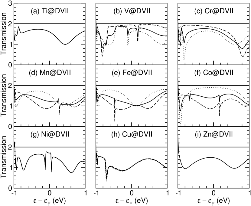
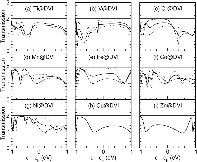
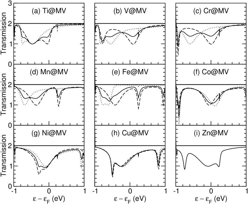
In the following sections, we will analyze the transmission data for the clean TM doped SWNTs. To aid our understanding we will also consider the DOS of the system, which drives the behavior we see in the transmission. We will first analyze all the different metals in the divancancy II, then the same will be done with the divacancy I and the monovacancy. Since we will concentrate on the DOS, it is important to understand the way the DOS and transmission T() are related. The peaks found in the DOS match with “dips” in the transmission, which are Fano anti-resonances [Furst]. While narrow peaks in the DOS denote localized states, broad peaks denote strong bonding or hybridized states.
5.1 Divacancy II
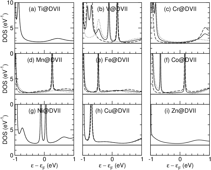
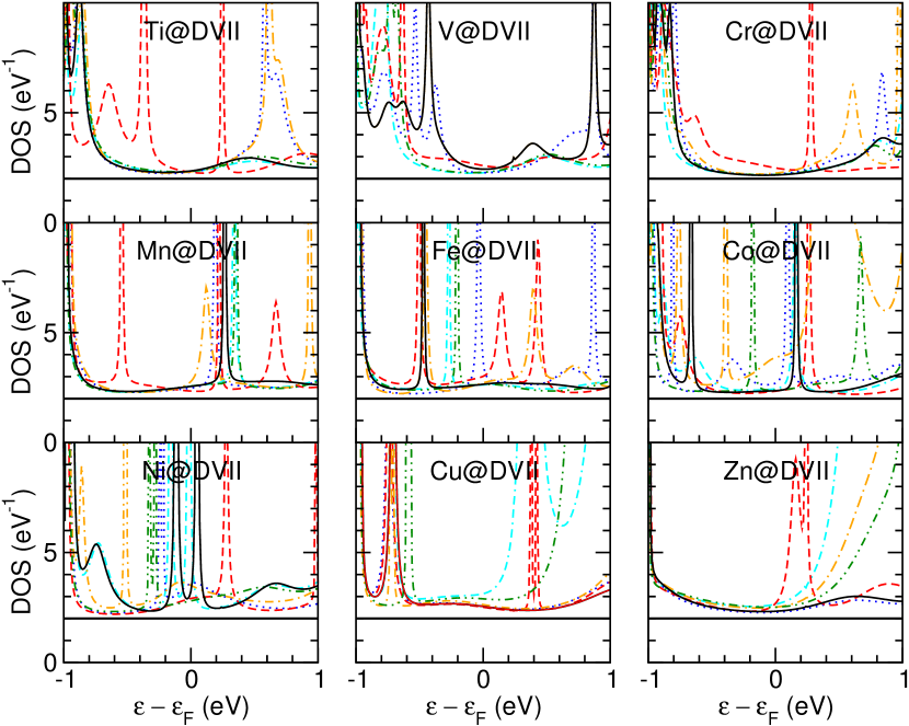
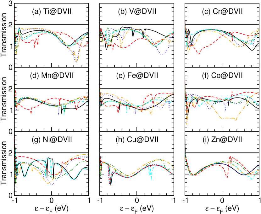
For a TM occupying a divacancy II (DVII) in a (6,6) SWNT (TM@DVII), shown schematically in Figure 4, there is an octahedral bonding of the TM atom, similar to the bonding in rutile metal oxides. Here, the TM bonding with the SWNT is through the two hybridized orbitals of the TM. From Figure 4 we see that all the TM–C bonds are equally strained by the curvature of the nanotube. This means that all TM–C bonds are equivalent. To put it in other words, there is one type of four-fold degenerate TM–C bonding state.
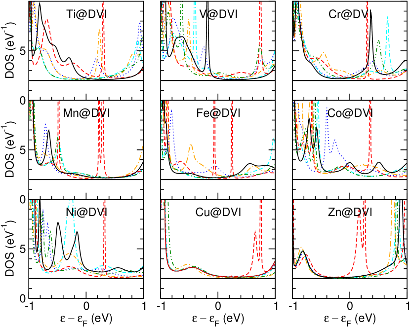
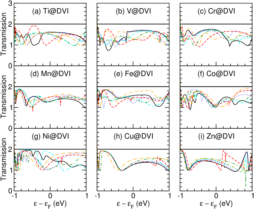
The DOS and transmission T through a pure TM occupied divacancy (TM@ DVII) are shown in Figures 9 and 10, respectively. As mentioned, if we compare the DOS and T shown in Figures 9 and 10, we find peaks and dips, respectively, relative to the flat DOS and T of a pristine (6,6) SWNT.
For Ti@DVII there are four occupied C —Ti bonds. These bonds are more than 1 eV below the Fermi level, so that they are not relevant for this study. There are also present completely unoccupied orbitals and anti-bonding Ti orbitals. However, only the orbitals of the TMs are important in the to 1 eV range. These orbitals are what determines the binding and transmission for the TM@DVII system.
In the case of V@DVII, there is one extra electron in the orbital, which is a non-bonding orbital. This extra electron yields a spin splitting in the DOS, as seen in Figure 9. The orbital is, by symmetry, non-bonding and it is localized on the V atom.
For Cr@DVII there are two extra electrons in the orbital, instead of only one. The states are shifted down in energy and there is no state around the Fermi level, as seen in Figure 9.
With Mn@DVII, electrons begin occupying the anti-bonding orbitals. There are then localized spin states above the Fermi level. These spin unpaired states, which are localized on the TM atom, move down in energy as they are filled with more -electrons. This is what we see in Figure 9 for Fe@DVII and Co@DVII.
For Ni@DVII, these localized states become spin-paired, with one of them being completely occupied, and the other one completely empty. When we add another electron to the band, moving to Cu@DVII, both states become fully occupied, localized on the Cu atom, and spin-paired.
Finally, for Zn@DVII, the -orbitals are now completely filled. The DOS closely resembles that of Ti@DVII, and the states are spin-paired, as shown in Figure 9.
5.2 Divacancy I
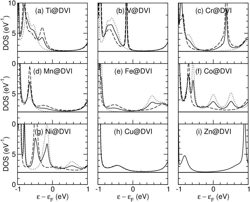
For a TM occupying a divacancy I (DVI) in a (6,6) SWNT (TM@DVI), shown schematically in Figure 4, the states are no longer as localized on the metal atom as for the TM@DVII, and are more strongly hybridized with the C states. Due to the geometric configuration of TM@DVI, the angle of two of the bonds with the axis of the nanotube is much smaller than the angle of the other two bonds. We will call these two different bonds near-axis and off-axis, respectively. This difference in the orientation produces a difference in the strain the bonds will have to withstand.
The off-axis bonds will undergo more stress due the SWNT’s curvature, compared to the near-axis bonds. This means that there are two types of degenerate TM–C bonding states. This degeneration results in a larger number of broader peaks and dips, compared to those obtained for a TM@DVII, as shown in Figures 11 and 12, respectively
Even with these differences it is still possible to see in Figure 11 the filling of states, and their movement to lower energy, exactly like in the case of the TM@DVII. It is very likely that the differences in the strain contribute to the splitting of the spin degeneracy for Ti@DVI and Ni@DVI.
The Ti@DVI orbitals are half-filled through bonding with the C orbitals, as is the 4 level. The Cu@DVI orbitals are filled by taking an electron from the 4 level. So, in the case of Cu@DVI, bonding occurs through the half-occupied 4 orbital. All of the Zn orbitals are completely filled, as is the 4 level. For these three systems, the DOS shown in Figure 11 is very similar to that shown in Figure 9 for the TM@DVII case. However, for the Ti@DVI DOS there is a noticeable difference, most probably due to the differences in strain for the two types of C–TM bonds (near-axis and off-axis).
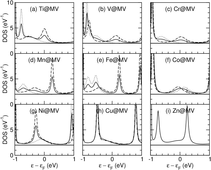
5.3 Monovacancy
For a TM occupying a monovacancy (MV) in a (6,6) SWNT (TM@MV), shown schematically in Figure 4, the TM atom has three bonds with three C atoms, two of the bonds being shorter, stronger, and near-axis, and one longer, weaker, and perpendicular to the nanotube axis. Not only is this bond weaker, but it is also the one that withstands the largest strain. From Figure 13 we see that for Ti@MV and Ni@MV we have spin splitting, which may be attributable to the strain in the weaker C–TM bond. Figure 13 also shows that for the monovacancy the DOS shifts down in energy as the orbitals on the TM atom are filled. The differences between the bond lengths and strengths of the three C–TM bonds yields several broad peaks in the DOS, as seen in Figure 13, and likewise broad dips in the transmission, as seen in Figure 14.
As shown in Figure 13, for Ti@MV, V@MV, and Cr@MV, we see a broad spin-unpaired peak centered near the Fermi level. This peak is shifted down in energy for Mn@MV, which has five electrons. At this point a narrower peak, for a -state more localized on the TM atom enters the energy window and it is positioned at round 0.2 eV. This state broadens for Co@MV where it is partly occupied, and nearly spin-paired. For Ni@MV this state goes further down in energy relative to the Fermi level and becomes spin paired for Cu@MV and Zn@MV.
5.4 Target and Background Molecules
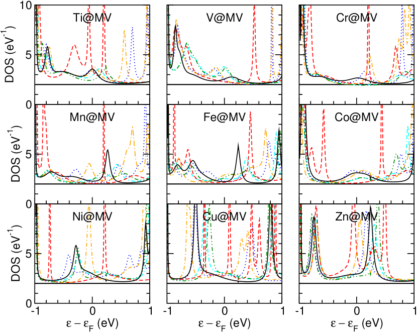
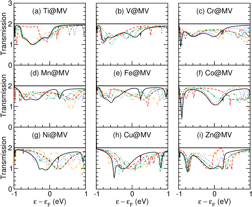
To estimate the effect of adsorbates on the electrical conductance of doped SWNTs, we first consider the change in conductance when a single molecule is adsorbed on a metal site of an otherwise pristine SWNT. In Figs. 15, 17, and 19 we show the calculated DOS for a TM occupied monovacancy, divacancy I, and divacancy II, respectively, with and without an adsorbed molecule . These may be compared with Figs. 16, 18, and 20 where we show the calculated transmission probability T for a TM occupied monovacancy, divacancy I, and divacancy II, respectively, with and without an adsorbed molecule .
In contrast to the adsorption energies, there are no clear trends in the conductances. The sensitivity of the conductance is perhaps most clearly demonstrated by the absence of correlation between different types of vacancies.
Close to the Fermi level, the conductance of a perfect armchair SWNT equals 2. The presence of the metal dopant leads to several dips in the transmission function known as Fano anti-resonances [Furst]. The position and shape of these dips depends on the -levels of the TM atom, the character of its bonding to the SWNT, and is further affected by the presence of the adsorbate molecule. The coupling of all these factors is very complex and makes it difficult to estimate or rationalize the value of the conductance. For the spin-polarized cases, we use the spin-averaged conductances, i.e. .
Cu@DVI binds all molecules rather weakly, so any changes in the DOS from the clean Cu@DVI structure between and 1 eV are attributable to states completely localized on the molecule. Here we only see two states localized on the O2 molecule between 0.6 and 0.8 eV above the Fermi level. For CO+Cu@DVI we see a shifting of the DOS, and hybridization with the Cu@DVI states. In particular, the broad peak below in the Cu@DVI DOS, which is binding with the C states, is shifted down in energy by about 0.1 eV when CO is adsorbed on the Cu@DVI site.
For O2, its ground state has spin 2, with one electron occupying a — anti-bonding orbital, and the other electron occupying a — anti-bonding orbital [cnt_networks]. For O2 on Ti@DVI, V@DVI, and Cr@DVI, the — anti-bonding orbital hybridizes with the transition metal atom’s state, leaving the spin down component of the other — anti-bonding state on the molecule unoccupied. This state is visible as a sharp peak above the Fermi level. By symmetry the — anti-bonding O2 state cannot bond to the TM@DVI system.
It should be noted that O2 is the only molecule with molecular states in the to +1 eV range relative to the (6,6) SWNT Fermi level. The O2 — anti-bonding states by symmetry are forbidden from bonding with the TM@DVI and TM@DVII systems. On the other hand, the O2 — anti-bonding state overlaps with the TM state. For Cu and Zn, as the orbitals are filled, we find the O2 anti-bonding states are both spin unpaired, and exhibit little hybridization with the TM@VC site.
Overall, the TM states are shifted up and down in energy when a molecule is adsorbed, based on both charge transfer, and the symmetry of the molecule’s orbitals. This leads to a rich response in the DOS of the TM@VC system upon adsorption of a molecule. The main conclusion to be made is that the DOS and thus the transmission through the TM@VC systems are quite sensitive to the adsorption of a molecule, and give a strong response. This makes the resistance through such active sites an excellent sensing property.
6 Sensing Property

The final “piece of the puzzle” for our model of a chemical nanosensor is the description of the sensing property, i.e. the change in resistance upon adsorption of a molecule under atmospheric conditions, via basic circuit theory, as depicted in Figure 21. At this point we bring together the transmission T calculated from the NEGF method and the coverage of active sites from the kinetic model to describe the change in resistance through the doped SWNT as a function of the target molecule’s concentration .
| Ti | V | Cr | Mn | Fe | Co | Ni | Cu | Zn | |
|---|---|---|---|---|---|---|---|---|---|
| N2 | 1.44 | 1.63 | 1.44 | 1.72 | 1.88 | 1.19 | 1.40 | 0.97 | 1.16 |
| O2 | 1.44 | 1.78 | 1.72 | 1.66 | 1.56 | 1.83 | 1.33 | 1.13 | 1.69 |
| H2O | 1.42 | 1.31 | 1.64 | 1.39 | 1.50 | 1.47 | 1.18 | 0.97 | 0.99 |
| CO | 1.31 | 1.61 | 1.61 | 1.59 | 1.33 | 1.09 | 1.58 | 0.97 | 1.79 |
| NH3 | 1.57 | 1.37 | 1.68 | 1.47 | 1.51 | 1.50 | 1.39 | 1.05 | 1.01 |
| H2S | 1.40 | 1.51 | 1.64 | 1.51 | 1.50 | 1.43 | 1.32 | 0.98 | 1.13 |
| Clean | 1.40 | 1.41 | 1.38 | 1.77 | 1.87 | 1.08 | 1.06 | 1.31 | 1.02 |
| Ti | V | Cr | Mn | Fe | Co | Ni | Cu | Zn | |
|---|---|---|---|---|---|---|---|---|---|
| N2 | 1.52 | 1.69 | 1.60 | 1.38 | 1.20 | 1.16 | 1.06 | 1.28 | 1.42 |
| O2 | 1.13 | 1.24 | 1.54 | 1.51 | 1.48 | 1.09 | 1.33 | 1.28 | 1.30 |
| H2O | 1.50 | 1.52 | 1.69 | 1.27 | 1.49 | 1.07 | 1.83 | 1.25 | 1.44 |
| CO | 1.58 | 1.29 | 1.28 | 1.50 | 1.74 | 1.13 | 1.56 | 1.50 | 1.48 |
| NH3 | 1.50 | 1.25 | 1.68 | 1.27 | 1.42 | 1.14 | 1.05 | 1.35 | 1.51 |
| H2S | 1.51 | 1.59 | 1.69 | 1.31 | 1.43 | 1.11 | 1.03 | 1.29 | 1.47 |
| Clean | 1.61 | 1.65 | 1.73 | 1.29 | 1.57 | 1.02 | 1.57 | 1.25 | 1.34 |
| Ti | V | Cr | Mn | Fe | Co | Ni | Cu | Zn | |
|---|---|---|---|---|---|---|---|---|---|
| N2 | 1.65 | 1.77 | 1.65 | 1.27 | 1.12 | 1.33 | 0.51 | 1.06 | 1.49 |
| O2 | 1.65 | 1.29 | 1.47 | 1.54 | 1.15 | 1.49 | 1.00 | 1.04 | 1.34 |
| H2O | 1.57 | 1.67 | 1.69 | 1.20 | 1.21 | 1.45 | 1.29 | 1.02 | 1.56 |
| CO | 1.68 | 1.79 | 1.52 | 1.29 | 1.07 | 0.61 | 0.69 | 1.17 | 1.56 |
| NH3 | 1.61 | 1.69 | 1.67 | 1.19 | 1.18 | 1.50 | 0.86 | 1.01 | 1.60 |
| H2S | 1.62 | 1.71 | 1.65 | 1.23 | 1.15 | 1.43 | 0.79 | 1.06 | 1.58 |
| Clean | 1.60 | 1.78 | 1.71 | 1.22 | 1.06 | 1.41 | 1.71 | 1.04 | 1.49 |
We now estimate the resistance of a SWNT containing several impurities (a specific metal dopant with different molecular adsorbates). Under the assumption that the electron phase-coherence length, , is smaller than the average distance between the dopants, , we may neglect quantum interference and obtain the total resistance by adding the scattering resistances due to each impurity separately. The scattering resistance due to a single impurity is then given by
| (22) |
Here is the Landauer conductance of the pristine SWNT with a single metal dopant occupied by molecule , i.e. the transmission at the Fermi level , is the contact resistance of a (6,6) SWNT, and is the quantum of conductance. The calculated conductances are provided in Tables 8, 9, and 10 for a molecule adsorbed on a TM occupied monovacancy, divacancy I, and divacancy II, respectively.
We may now obtain the average change in resistance of an active site as a function of target molecule concentration. As discussed in Ref. [Juanma], this change in resistance is reasonably well described by
| (23) |
where is the concentration, and is the concentration at standard temperature and pressure, as given in Table 4.
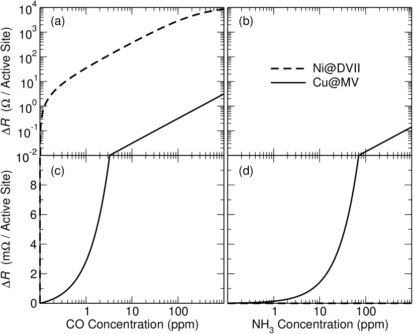
In Figure 22 we show for a single active site (Ni or Cu) as a function of target molecule concentration (CO or NH3). Keeping in mind that a change in concentration from 1 ppm to 50 ppm amounts to a change from allowable to toxic concentrations for both CO and NH3, we see that this sensor design should work effectively for both target molecules.
7 Conclusions
In summary, we have presented a general model for the design of chemical nanosensors which takes the adsorption energies of the relevant chemical species and their individual scattering resistances as the only input. On the basis of this model we have performed a computational screening of TM doped SWNTs, and demonstrated using ab initio calculations how a combined Cu and Ni doped metallic SWNT device may work effectively as a multifunctional sensor for both CO and NH3. Further, we find that by varying the metal dopant, we obtain “another handle” for tuning the sensitivity of our sensor. The methodology employed may also be applied to other nanosensor designs and different environments, and demonstrates the potential of computational screening studies for the design of chemical nanosensors in silico.
Acknowledgments
We acknowledge funding through the European Research Council Advanced Grant DYNamo (ERC-2010-AdG -Proposal No. 267374), Spanish “Juan de la Cierva” and José Castillejo programs (JCI-2010-08156), Spanish Ministerio de Ciencia e Innovacíon (FIS2010-21282-C02-01, FIS2010-19609-C02-01), Spanish “Grupos Consolidados UPV/EHU del Gobierno Vasco” (IT-319-07, IT-366-07), and ACI-Promociona (ACI2009-1036), ARINA, NABIIT and the Danish Center for Scientific Computing. The Center for Atomic-scale Materials Design (CAMD) is sponsored by the Lundbeck Foundation.
References
- [1] \harvarditem[Arnold et al.]Arnold, Green, Hulvat, Stupp, and Hersam2006Arnold06NN Arnold M. S., Green A. A., Hulvat J. F., Stupp S. I., and Hersam M. C. \harvardyearleft2006\harvardyearright Sorting carbon nanotubes by electronic structure using density differentiation. Nature Nanotechnology 1(1), 60.
- [2] \harvarditemAshcroft, and Mermin1976Ashcroft Ashcroft N. W., and Mermin N. D. \harvardyearleft1976\harvardyearright Solid State Physics. Thomson Learning. Toronto.
- [3] \harvarditem[Ayala et al.]Ayala, Arenal, Loiseau, Rubio, and Pichler2010PaolaRevModPhys Ayala P., Arenal R., Loiseau A., Rubio A., and Pichler T. \harvardyearleft2010\harvardyearright The physical and chemical properties of heteronanotubes. Rev. Mod. Phys. 82, 1843–1885.
- [4] \harvarditem[Ayala et al.]Ayala, Grueneis, Gemming, Grimm, Kramberger, Ruemmeli, Freire, Kuzmany, Pfeiffer, Barreiro, Buechner, and Pichler2007PaolaNdopedCNTs Ayala P., Grueneis A., Gemming T., Grimm D., Kramberger C., Ruemmeli M. H., Freire, Jr. F. L., Kuzmany H., Pfeiffer R., Barreiro A., Buechner B., and Pichler T. \harvardyearleft2007\harvardyearright Tailoring N-doped single and double wall carbon nanotubes from a nondiluted carbon/nitrogen feedstock. J. Phys. Chem C 111(7), 2879–2884.
- [5] \harvarditem[Ayala et al.]Ayala, Miyata, De Blauwe, Shiozawa, Feng, Yanagi, Kramberger, Silva, Follath, Kataura, and Pichler2009Ayala09PRB Ayala P., Miyata Y., De Blauwe K., Shiozawa H., Feng Y., Yanagi K., Kramberger C., Silva S. R. P., Follath R., Kataura H., and Pichler T. \harvardyearleft2009\harvardyearright Disentanglement of the electronic properties of metallicity-selected single-walled carbon nanotubes. Phys. Rev. B 80(20), 205427.
- [6] \harvarditem[Ayala et al.]Ayala, Plank, Grueneis, Kauppinen, Ruemmeli, Kuzmany, and Pichler2008PaolaBdopedCNTs Ayala P., Plank W., Grueneis A., Kauppinen E. I., Ruemmeli M. H., Kuzmany H., and Pichler T. \harvardyearleft2008\harvardyearright A one step approach to B-doped single-walled carbon nanotubes. J. Mater. Chem. 18(46), 5676–5681.
- [7] \harvarditemBlöchl1994Blochl Blöchl P. E. \harvardyearleft1994\harvardyearright Projector augmented-wave method. Phys. Rev. B 50, 17953–17979.
- [8] \harvarditem[Brahim et al.]Brahim, Colbern, Gump, and Grigorian2008Brahim Brahim S., Colbern S., Gump R., and Grigorian L. \harvardyearleft2008\harvardyearright Tailoring gas sensing properties of carbon nanotubes. J. Appl. Phys. 104(2), 024502.
- [9] \harvarditem[Chalier et al.]Chalier, Blase, and Roche2007cnt_review Chalier J. C., Blase X., and Roche S. \harvardyearleft2007\harvardyearright Electronic and transport properties of nanotubes. Rev. Mod. Phys. 79(2), 677.
- [10] \harvarditem[Chan et al.]Chan, Neaton, and Cohen2008Chan Chan K. T., Neaton J. B., and Cohen M. L. \harvardyearleft2008\harvardyearright First-principles study of metal adatom adsorption on graphene. Phys. Rev. B 77(23), 235430.
- [11] \harvarditem[Charlier et al.]Charlier, Blase, and Roche2007RevModPhys.79.677 Charlier J.-C., Blase X., and Roche S. \harvardyearleft2007\harvardyearright Electronic and transport properties of nanotubes. Rev. Mod. Phys. 79, 677–732.
- [12] \harvarditem[Collins et al.]Collins, Bradley, Ishigami, and Zettl2000collins Collins P. G., Bradley K., Ishigami M., and Zettl A. \harvardyearleft2000\harvardyearright Extreme oxygen sensitivity of electronic properties of carbon nanotubes. Science 287(5459), 1801.
- [13] \harvarditemDatta1997Datta Datta S. \harvardyearleft1997\harvardyearright Electronic Transport in Mesoscopic Systems. 1 edn. Cambridge University Press. Cambridge.
- [14] \harvarditem[De Blauwe et al.]De Blauwe, Miyata, Ayala, Shiozawa, Mowbray, Rubio, Hoffmann, Kataura, and Pichler2010DeBlauwe2010 De Blauwe K., Miyata Y., Ayala P., Shiozawa H., Mowbray D. J., Rubio A., Hoffmann P., Kataura H., and Pichler T. \harvardyearleft2010\harvardyearright A combined PES and ab-initio study of the electronic structure of (6,5)/(6,4) enriched single wall carbon nanotubes. Phys. Status Solidi B 247(11-12), 2875–2879.
- [15] \harvarditem[Dresselhaus et al.]Dresselhaus, Dresselhaus, and Avouris2001Dresselhaus Dresselhaus, M. S., Dresselhaus, G., and Avouris, P. (eds) \harvardyearleft2001\harvardyearright Carbon Nanotubes: Synthesis, Structure, Properties, and Applications. Springer. Berlin.
- [16] \harvarditemEngel, and Dreizler2011DFT2011 Engel E., and Dreizler R. M. \harvardyearleft2011\harvardyearright Density Functional Theory: An Advanced Course. Springer-Verlag. Berlin.
- [17] \harvarditem[Enkovaara et al.]Enkovaara, Rostgaard, Mortensen, Chen, Dułak, Ferrighi, Gavnholt, Glinsvad, Haikola, Hansen, Kristoffersen, Kuisma, Larsen, Lehtovaara, Ljungberg, Lopez-Acevedo, Moses, Ojanen, Olsen, Petzold, Romero, Stausholm-Møller, Strange, Tritsaris, Vanin, Walter, Hammer, Häkkinen, Madsen, Nieminen, Nørskov, Puska, Rantala, Schiøtz, Thygesen, and Jacobsen2010GPAWRev Enkovaara J., Rostgaard C., Mortensen J. J., Chen J., Dułak M., Ferrighi L., Gavnholt J., Glinsvad C., Haikola V., Hansen H. A., Kristoffersen H. H., Kuisma M., Larsen A. H., Lehtovaara L., Ljungberg M., Lopez-Acevedo O., Moses P. G., Ojanen J., Olsen T., Petzold V., Romero N. A., Stausholm-Møller J., Strange M., Tritsaris G. A., Vanin M., Walter M., Hammer B., Häkkinen H., Madsen G. K. H., Nieminen R. M., Nørskov J. K., Puska M., Rantala T. T., Schiøtz J., Thygesen K. S., and Jacobsen K. W. \harvardyearleft2010\harvardyearright Electronic structure calculations with GPAW: a real-space implementation of the projector augmented-wave method. J. Phys.: Condens. Matter 22, 253202.
- [18] \harvarditem[Fagan et al.]Fagan, Simpson, Bauer, Lacerda, Becker, Chun, Migler, Walker, and Hobbie2007Fagan07JOTACS Fagan J. A., Simpson J. R., Bauer B. J., Lacerda S. H. D., Becker M. L., Chun J., Migler K. B., Walker A. R. H., and Hobbie E. K. \harvardyearleft2007\harvardyearright Length-dependent optical effects in single-wall carbon nanotubes. J. Amer. Chem. Soc. 129(34), 10607.
- [19] \harvarditem[Fagan et al.]Fagan, Mota, da Silva, and Fazzio2003Fagan Fagan S. B., Mota R., da Silva A. J. R., and Fazzio A. \harvardyearleft2003\harvardyearright Ab initio study of an iron atom interacting with single-wall carbon nanotubes. Phys. Rev. B 67(20), 205414.
- [20] \harvarditem[Fiolhais et al.]Fiolhais, Nogueira, and Marques2003DFTMarques Fiolhais, C., Nogueira, F., and Marques, M. (eds) \harvardyearleft2003\harvardyearright A Primer in Density Functional Theory. Lecture notes in physics. Springer-Verlag. Berlin.
- [21] \harvarditem[Fürst et al.]Fürst, Brandbyge, Jauho, and Stokbro2008Furst Fürst J. A., Brandbyge M., Jauho A.-P., and Stokbro K. \harvardyearleft2008\harvardyearright Ab initio study of spin-dependent transport in carbon nanotubes with iron and vanadium adatoms. Phys. Rev. B 78(19), 195405.
- [22] \harvarditem[García-Lastra et al.]García-Lastra, Mowbray, Thygesen, Rubio, and Jacobsen2010Juanma García-Lastra J. M., Mowbray D. J., Thygesen K. S., Rubio Á., and Jacobsen K. W. \harvardyearleft2010\harvardyearright Modeling nanoscale gas sensors under realistic conditions: Computational screening of metal-doped carbon nanotubes. Phys. Rev. B 81(24), 245429.
- [23] \harvarditem[García-Lastra et al.]García-Lastra, Thygesen, Strange, and Ángel Rubio2008JuanmaPRL García-Lastra J. M., Thygesen K. S., Strange M., and Ángel Rubio \harvardyearleft2008\harvardyearright Conductance of sidewall-functionalized carbon nanotubes: Universal dependence on adsorption sites. Phys. Rev. Lett. 101(23), 236806.
- [24] \harvarditem[Goldoni et al.]Goldoni, Petaccia, Gregoratti, Kaulich, Barinov, Lizzit, Laurita, Sangaletti, and Larciprete2004Goldoni Goldoni A., Petaccia L., Gregoratti L., Kaulich B., Barinov A., Lizzit S., Laurita A., Sangaletti L., and Larciprete R. \harvardyearleft2004\harvardyearright Spectroscopic characterization of contaminants and interaction with gases in single-walled carbon nanotubes. Carbon 42(10), 2099–2112.
- [25] \harvarditemGriffith1961Griffith Griffith J. S. \harvardyearleft1961\harvardyearright The Theory of Transition-Metal Ions. Cambridge University Press. London.
- [26] \harvarditemHarris1999Harris Harris P. J. F. \harvardyearleft1999\harvardyearright Carbon Nanotubes and Related Structures: New Materials for the Twenty-first Century. Cambridge University Press. Cambridge.
- [27] \harvarditemHierold2008hierold Hierold C. \harvardyearleft2008\harvardyearright Carbon Nanotube Devices: Properties, Modeling, Integration and Applications. Wiley-VCH. Weinheim.
- [28] \harvarditemIijima1991Iijima Iijima S. \harvardyearleft1991\harvardyearright Helical microtubules of graphitic carbon. Nature 354, 56–58.
- [29] \harvarditem[Jensen et al.]Jensen, Kim, and Zettl2008ZettlMassSensor Jensen K., Kim K., and Zettl A. \harvardyearleft2008\harvardyearright An atomic-resolution nanomechanical mass sensor. Nature Nanotech. 3, 533–537.
- [30] \harvarditem[Jin et al.]Jin, Lan, Suenaga, Peng, and Iijima2008Chuanhong Jin C., Lan H., Suenaga K., Peng L., and Iijima S. \harvardyearleft2008\harvardyearright Metal atom catalyzed enlargement of fullerenes. Phys. Rev. Lett. 101(17), 176102.
- [31] \harvarditemKohn, and Sham1965Kohn-Sham Kohn W., and Sham L. J. \harvardyearleft1965\harvardyearright Self-consistent equations including exchange and correlation effects. Phys. Rev. 140, A1133–A1138.
- [32] \harvarditem[Kong et al.]Kong, Franklin, Zhou, Chapline, Peng, Cho, and Dai2000kong Kong J., Franklin N. R., Zhou C., Chapline M. G., Peng S., Cho K., and Dai H. \harvardyearleft2000\harvardyearright Nanotube molecular wires as chemical sensors. Science 287(5453), 622.
- [33] \harvarditem[Kramberger et al.]Kramberger, Rauf, Shiozawa, Knupfer, Buchner, Pichler, Batchelor, and Kataura2007Kramberger07PRB Kramberger C., Rauf H., Shiozawa H., Knupfer M., Buchner B., Pichler T., Batchelor D., and Kataura H. \harvardyearleft2007\harvardyearright Unraveling van hove singularities in x-ray absorption response of single-wall carbon nanotubes. Phys. Rev. B 75(23), 235437.
- [34] \harvarditem[Krasheninnikov et al.]Krasheninnikov, Lehtinen, Foster, Pyykkö, and Nieminen2009Krasheninnikov Krasheninnikov A. V., Lehtinen P. O., Foster A. S., Pyykkö P., and Nieminen R. M. \harvardyearleft2009\harvardyearright Embedding transition-metal atoms in graphene: Structure, bonding, and magnetism. Phys. Rev. Lett. 102(12), 126807.
- [35] \harvarditem[Lassagne et al.]Lassagne, Garcia-Sanchez, Aguasca, and Bachtold2008Bachtold Lassagne B., Garcia-Sanchez D., Aguasca A., and Bachtold A. \harvardyearleft2008\harvardyearright Ultrasensitive mass sensing with a nanotube electromechanical resonator. Nano Lett. 8(11), 3735.
- [36] \harvarditem[Li et al.]Li, Tu, Zaric, Welsher, Seo, Zhao, and Dai2007Li07JOTACS Li X. L., Tu X. M., Zaric S., Welsher K., Seo W. S., Zhao W., and Dai H. J. \harvardyearleft2007\harvardyearright Selective synthesis combined with chemical separation of single-walled carbon nanotubes for chirality selection. J. Amer. Chem. Soc. 129(51), 15770.
- [37] \harvarditemLide2006–2007CRCHandbook Lide D. \harvardyearleft2006–2007\harvardyearright Handbook of Chemistry and Physics. 87 edn. CRC-Press.
- [38] \harvarditemMeir, and Wingreen1992Meir Meir Y., and Wingreen N. S. \harvardyearleft1992\harvardyearright Landauer formula for the current through an interacting electron region. Phys. Rev. Lett 68(16), 2512–2515.
- [39] \harvarditem[Morgan et al.]Morgan, Alemipour, and Baxendale2008morgan Morgan C., Alemipour Z., and Baxendale M. \harvardyearleft2008\harvardyearright Variable range hopping in oxygen-exposed single-wall carbon nanotube networks. Phys. Stat. Solidi A 205(6), 1394.
- [40] \harvarditem[Mortensen et al.]Mortensen, Hansen, and Jacobsen2005GPAW Mortensen J. J., Hansen L. B., and Jacobsen K. W. \harvardyearleft2005\harvardyearright Real-space grid implementation of the projector augmented wave method. Phys. Rev. B 71(3), 035109.
- [41] \harvarditem[Mowbray et al.]Mowbray, García-Lastra, Thygesen, Rubio, and Jacobsen2010Kirchberg Mowbray D. J., García-Lastra J. M., Thygesen K. S., Rubio A., and Jacobsen K. W. \harvardyearleft2010\harvardyearright Designing multifunctional chemical sensors using Ni and Cu doped carbon nanotubes. Phys. Status Solidi B 247(11-12), 2678–2682.
- [42] \harvarditem[Mowbray et al.]Mowbray, Morgan, and Thygesen2009cnt_networks Mowbray D. J., Morgan C., and Thygesen K. S. \harvardyearleft2009\harvardyearright Influence of O2 and N2 on the conductivity of carbon nanotube networks. Phys. Rev. B 79(19), 195431.
- [43] \harvarditemParr, and Yang1989Parr Parr R. G., and Yang W. \harvardyearleft1989\harvardyearright Density-Functional Theory of Atoms and Molecules. Oxford University Press. New York.
- [44] \harvarditem[Perdew et al.]Perdew, Burke, and Ernzerhof1996PBE Perdew J. P., Burke K., and Ernzerhof M. \harvardyearleft1996\harvardyearright Generalized gradient approximation made simple. Phys. Rev. Lett. 77(18), 3865.
- [45] \harvarditem[Rocha et al.]Rocha, Rossi, Fazzio, and da Silva2008rocha Rocha A. R., Rossi M., Fazzio A., and da Silva A. J. R. \harvardyearleft2008\harvardyearright Designing real nanotube-based gas sensors. Phys. Rev. Lett. 100(17), 176803.
- [46] \harvarditem[Sánchez-Portal et al.]Sánchez-Portal, Artacho, Soler, Rubio, and Ordejón1999Rubio1 Sánchez-Portal D., Artacho E., Soler J. M., Rubio A., and Ordejón P. \harvardyearleft1999\harvardyearright Ab initio structural, elastic, and vibrational properties of carbon nanotubes. Phys. Rev. B 59(19), 12678–12688.
- [47] \harvarditem[Soler et al.]Soler, Artacho, Gale, Garcia, Junquera, Ordejón, and Sánchez-Portal2002SIESTA Soler J. M., Artacho E., Gale J. D., Garcia A., Junquera J., Ordejón P., and Sánchez-Portal D. \harvardyearleft2002\harvardyearright The SIESTA method for ab initio order- materials simulation. J. Phys.: Condens. Matter 14(11), 2745.
- [48] \harvarditem[Strange et al.]Strange, Kristensen, Thygesen, and Jacobsen2008BenchmarkPaper Strange M., Kristensen I. S., Thygesen K. S., and Jacobsen K. W. \harvardyearleft2008\harvardyearright Benchmark density functional theory calculations for nanoscale conductance. J. Chem. Phys. 128(11), 114714.
- [49] \harvarditemThygesen2006Thygesen2 Thygesen K. S. \harvardyearleft2006\harvardyearright Electron transport through an interacting region: The case of a nonorthogonal basis set. Phys. Rev. B 73(3), 035309.
- [50] \harvarditem[Tu et al.]Tu, Manohar, Jagota, and Zheng2009TU09N Tu X. M., Manohar S., Jagota A., and Zheng M. \harvardyearleft2009\harvardyearright DNA sequence motifs for structure-specific recognition and separation of carbon nanotubes. Nature 460(7252), 250.
- [51] \harvarditem[Valentini et al.]Valentini, Mercuri, Armentano, Cantalini, Picozzi, Lozzi, Santucci, Sgamellotti, and Kenny2004Valentini2004356 Valentini L., Mercuri F., Armentano I., Cantalini C., Picozzi S., Lozzi L., Santucci S., Sgamellotti A., and Kenny J. M. \harvardyearleft2004\harvardyearright Role of defects on the gas sensing properties of carbon nanotubes thin films: experiment and theory. Chem. Phys. Lett. 387(4-6), 356 – 361.
- [52] \harvarditem[Villalpando-Páez et al.]Villalpando-Páez, Romero, Muñoz-Sandoval, Martínez, Terrones, and Terrones2004villalpando Villalpando-Páez F., Romero A. H., Muñoz-Sandoval E., Martínez L. M., Terrones H., and Terrones M. \harvardyearleft2004\harvardyearright Fabrication of vapor and gas sensors using films of aligned CNx nanotubes. Chem. Phys. Lett. 386(1-3), 137.
- [53] \harvarditem[Vo et al.]Vo, Wu, Car, and Robert2008Vo Vo T., Wu Y.-D., Car R., and Robert M. \harvardyearleft2008\harvardyearright Structures, interactions, and ferromagnetism of Fe-carbon nanotube systems. J. Phys. Chem. C 112(22), 400.
- [54] \harvarditem[Yagi et al.]Yagi, Briere, Sluiter, Kumar, Farajian, and Kawazoe2004Yagi Yagi Y., Briere T. M., Sluiter M. H. F., Kumar V., Farajian A. A., and Kawazoe Y. \harvardyearleft2004\harvardyearright Stable geometries and magnetic properties of single-walled carbon nanotubes doped with transition metals: A first-principles study. Phys. Rev. B 69(7), 075414.
- [55] \harvarditem[Yang et al.]Yang, Shin, Lee, Kim, Woo, and Kang2006Yang Yang S. H., Shin W. H., Lee J. W., Kim S. Y., Woo S. I., and Kang J. K. \harvardyearleft2006\harvardyearright Interaction of a transition metal atom with intrinsic defects in single-walled carbon nanotubes. J. Phys. Chem. B 110(28), 13941.
- [56] \harvarditem[Yeung et al.]Yeung, Liu, and Wang2008Yeung Yeung C. S., Liu L. V., and Wang Y. A. \harvardyearleft2008\harvardyearright Adsorption of small gas molecules onto Pt-doped single-walled carbon nanotubes. J. Phys. Chem. C 112(19), 7401.
- [57] \harvarditemZanolli, and Charlier2009zanolli:155447 Zanolli Z., and Charlier J.-C. \harvardyearleft2009\harvardyearright Defective carbon nanotubes for single-molecule sensing. Phys. Rev. B 80(15), 155447.
- [58] \harvarditemZheng et al.2003aZheng03NM Zheng M., Jagota A., Semke E. D., Diner B. A., Mclean R. S., Lustig S. R., Richardson R. E., and Tassi N. G. \harvardyearleft2003\harvardyearright DNA-assisted dispersion and separation of carbon nanotubes. Nature Materials 2(5), 338.
- [59] \harvarditemZheng et al.2003bZheng03S Zheng M., Jagota A., Strano M. S., Santos A. P., Barone P., Chou S. G., Diner B. A., Dresselhaus M. S., McLean R. S., Onoa G. B., Samsonidze G. G., Semke E. D., Usrey M., and Walls D. J. \harvardyearleft2003\harvardyearright Structure-based carbon nanotube sorting by sequence-dependent DNA assembly. Science 302(5650), 1545.
- [60]