Anomalous Suppression of Valley Splittings in Lead Salt Nanocrystals without Inversion Center
Abstract
Atomistic tight-binding theory of PbSe and PbS nanocrystals is developed. It is demonstrated, that the valley splittings of confined electrons and holes strongly and peculiarly depend on the geometry of a nanocrystal. When the nanocrystal lacks a microscopic center of inversion and has symmetry, the splitting is strongly suppressed as compared to the more symmetric nanocrystals with symmetry, having an inversion center.
pacs:
71.35.-y, 71.36.+c, 42.70.QsInterest in almost spherical nanocrystals (NCs) made of lead chalcogenides (PbSe, PbS) has recently exploded due to their utility in fundamental studies of quantum confinement effects and enabling potential for technological applications in photovoltaics Ellingson et al. (2005); Schaller and Klimov (2004); Trinh et al. (2008); Beard et al. (2009). These applications impose requirements of reproducibility of the devices, ability to control their properties and necessity to understand mechanisms behind physical processes underlying their work. It has been noted Allan and Delerue (2004); An et al. (2006) that lead salt NCs are very peculiar compared to quantum dots (QDs) of III-V and II-VI compound semiconductors because lead chalcogenides have band extrema in the four inequivalent -points of the Brillouin zone and such effects as confinement-induced valley-mixing and effective mass anisotropy should be considered to fully account for the properties of lead salt NCs. It also was suggested that optical properties of lead salt NC QDs can be sensitive to a particular arrangement of atoms within the QD, as the latter determines the overall symmetry of the structure Goupalov (2009); Nootz et al. (2010).
In this work we study how all these effects influence the valley-orbit and spin-orbit splittings of one-particle energy levels of electrons and holes confined in lead salt NCs using the atomistic tight-binding (TB) approach. We found that these splittings are very sensitive to the particular arrangement of atoms within the almost spherical NC. In particular, we considered NCs of almost spherical shape centered on an anion or cation atom, serving as a center of inversion, along with NCs having no inversion symmetry. We found that in NCs without a center of inversion the valley-orbit and spin-orbit splittings of electron energy levels are strongly suppressed. This effect is quite unusual because typically a higher symmetry of a physical system implies a higher degeneracy of its energy levels, while in our case the suppression of the splittings occurs in NCs having lower symmetry. Nevertheless, we were able to explain this puzzling behavior using mathematical apparatus of the group theory.
Lead chalcogenides (PbSe, PbS) are semiconductor compounds with a rocksalt crystal lattice and a narrow and direct band gap Kang and Wise (1997). The extrema of both the conduction and valence bands are located at the four -points of the Brillouin zone:
| (1) |
where is the lattice constant. The empirical TB method is an efficient tool to model electronic properties of large-scale nanostructures Delerue and Lanoo (2004). Success of the TB parametrization depends on the choice of basis functions and on the accuracy of the fit of the bulk band structure. The simplest TB parametrizations of lead chalcogenides are based on the basis set of the three orbitals playing major role in the formation of the valence and conduction band states Mitchell and Wallis (1966); Volkov et al. (1983). More quantitatively accurate models include also and orbitals Lent et al. (1986); Lach-hab et al. (2002); Valdivia and Barberis (1995); Allan and Delerue (2004). However, no attempts (with the only exception of Ref. Volkov et al. (1983)) have been made to fit the actual effective masses of the electrons and holes near the -points. On the other hand, the second-nearest neighbors model of Ref. Volkov et al. (1983) fails to reproduce the bulk dispersion for wavevectors far from the points An et al. (2006). Consequently, even the most advanced existing TB parametrizations of lead chalcogenidesAllan and Delerue (2004) are not suitablePaul and Klimeck (2011) for an adequate description of the NCs.
We have performed an independent atomistic TB parametrization of the electron energy dispersion in bulk PbSe and PbS by fitting the spectra calculated by the state-of-the art GW technique of Ref. Svane et al. (2010). The goal values for the carrier effective masses near the -points were set to the experimental values Preier (1979): for PbSe and for PbS ( is the free electron mass), as even the modern ab initio approachSvane et al. (2010) does not satisfactory reproduce the effective masses.
| PbS | PbSe | |
|---|---|---|
| , Å | ||
| PbS | PbSe | |
|---|---|---|
The TB parameters we obtained are listed in Table 1. The resulting effective masses for PbSe and for PbS are quite close to the experimental values. The spin-orbit coupling constants of orbitals at Pb, Se, and S were not changed during the fitting procedure and were taken from Refs. Herman et al. (1963) and Herman and Skillman (1963) for Pb and for the anions, respectively.
In our study we will consider the three types of NC geometries illustrated in Fig. 1.
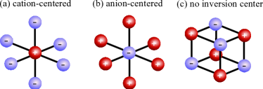

For the structures shown in Figs. 1a(b) the center of the spherical NC is on a cation (anion) atom while for the structure in Fig. 1c the center of the sphere lies halfway between a cation and an anion on a line parallel to the direction. The non-stoichiometric QDs of the types (a) and (b) both have centers of inversion and are characterized by the cube symmetry group . The stoichiometric QD of the type (c) has no inversion center and is characterized by the tetrahedron symmetry group . Note that the QDs cannot be perfectly spherical due to the discretness and lower point symmetry of the underlying crystal lattice. In our work the QDs are formed by all the atoms within a certain distance from the center of the NC. It is convenient to measure this distance with a dimensionless integer number. Thus, we define the “number of shells” as the number of atomic layers within the distance from the center of the QD to its surface along the direction.
Contrary to covalent semiconductors like Si Allan and Delerue (2004), lead chalcogenides are characterized by the strongly ionic atomic bonds making them relatively insensitive to the surface chemistry Paul and Klimeck (2011). In particular, no surface states appear in the fundamental band gap of non-passivated lead chalcogenide NCs. Therefore, we have not passivated the surface atoms in our TB modeling. In real QDs of the types (a) and (b) (cf. Fig. 1) such passivation is necessary to compensate for the surface charge Leitsmann and Bechstedt (2009). The actual structure of the NCs should depend on the details of the synthesis procedure and can be determined with the help of the nuclear magnetic resonanceMoreels et al. (2008) and X-ray diffractionPetkov et al. (2010) techniques.
The calculated energy levels of confined carriers for PbSe and PbS NCs of the diameter nm (corresponding to 9 shells) are shown in Fig. 2. For each material three panels (a–c and a′–c′) correspond to the three possible NC geometries illustrated in Fig. 1. The band gap in both cases agrees well with the results of Ref. Allan and Delerue (2004).
All the states can be divided into distinct groups characterized by a certain parity. For NCs with a center of inversion, each state automatically has a certain parity. Indeed, in bulk lead chalcogenides the lowest electron state in the conduction band has the symmetry Svane et al. (2010), i.e. it is odd with respect to the inversion symmetry operation when the center of inversion is chosen on the cation atom. The uppermost electron state in the valence band has the opposite parity. For QDs without an inversion center one can define approximate projectors to the even and odd states. We have attributed a certain parity to the states, for which the squared mean values of the projectors differed more than in three times.
Energy splittings within each multiplet characterized by a certain parity are clearly seen in Fig. 2 and can be explained by the confinement-induced inter-valley coupling and the carrier effective mass anisotropy. The importance of these two effects for lead chalcogenide NCs has been emphasized in Ref. An et al. (2006). However, the dependence of the splittings on the NC geometry clearly manifested in Fig. 2 has never been reported.
A striking feature of Fig. 2 is the suppression of the energy splittings for the type (c) NCs lacking a center of inversion. The splittings are quite small and cannot be distinguished within the energy scale of Fig 2. On the contrary, for QDs with an inversion center [panels (a), (b), (a′), (b′) of Fig. 2], the ground-state multiplets for both electrons and holes have well-pronounced structures with substantial splittings even for QD diameters as large as 4.9 nm. This observation refers to both the conduction and valence band electron states. The effect is more pronounced for the PbS QDs than for the PbSe QDs, which can be related to the more isotropic effective masses of the band extrema in bulk PbS.
To elucidate this puzzling behavior, we have analyzed the dependence of the splittings on the NC diameter. For simplicity, we restrict our consideration by the electron and hole ground states. Within the effective mass approximation, the ground state of confined carriers is fourfold degenerate with respect to the valley index and twofold degenerate with respect to the spin projection, i.e. the total degeneracy is eightfold. If we neglect the spin and consider valley-orbit interaction only, the ground state is split into a state of symmetry (singlet), and a state of symmetry (triplet), as sketched in insets of Figs. 3,4. When the spin degree of freedom is taken into account then both the singlet and the triplet states acquire extra degeneracy. This degeneracy is partly lifted, as the six-fold degenerate state corresponding to the triplet is split by the spin-orbit interaction into a two-fold degenerate state of symmetry and a four-fold degenerate state of symmetry Bir and Pikus (1974). As a result, the carrier ground-state level is split into the three multiplets: the two doublets (of and symmetry, respectively) and the four-fold degenerate state of symmetry. As far as the symmetry with respect to inversion is not concerned, the symmetry groups and are equivalent. Therefore, this symmetry analysis applies to all types of NC geometries presented in Fig. 1.
Figures 3 and 4 show the energies of the resulting conduction (valence) band multiplets in PbS NCs as functions of the NC diameter. The panels (a)–(c) correspond to the three NC geometries considered throughout the paper (see Fig. 1). The energies of the states are counted from the averaged value . The splittings strongly oscillate with the number of shells in a NC. Such oscillations are typical for the valley splittings in various semiconductor structures. Similar behavior has been reported for SiGe/SiNestoklon et al. (2006); Friesen et al. (2007) and GaSb/AlAsTing and Chang (1988); Jancu et al. (2004) quantum wells and Si NCs Bulutay (2007).


Comparison of panels (a) and (b) of Figs. 3,4 on one hand with the panels (c) of Figs. 3,4 on the other hand clearly shows that the suppression of valley splittings in NCs without a center of inversion is a general feature persistent in a wide range of NC sizes. Comparison of Fig. 3 with Fig. 4 enables one to conclude that the spin-orbit interaction is much stronger for conduction-band electrons than for valence-band holes. Indeed, the energies of the hole states with the symmetry and in Fig. 4 are almost the same, while, for conduction-band electrons, all the splittings in Fig. 3 are of the same order.
Let us explain the anomalous suppression of the valley splittings in lead salt NCs without an inversion center. We want to account for the inter-valley coupling in the lowest non-vanishing approximation. To this end we consider electronic states originating from the four inequivalent valleys of a bulk semiconductor and neglect the mixing of conduction and valence band states Kang and Wise (1997). Then the wave function of the confined electron state in the -th -valley can be written as where is the smooth envelope function, is the periodic Bloch amplitude for the bulk state in the -th valley, and spin indices are omitted. We will further assume that the bulk material has isotropic effective masses of the band extrema in points. In this approximation the envelopes are invariant under rotations. The confinement-induced inter-valley coupling can be described by the following matrix element:
| (2) |
where is the microscopic QD Hamiltonian. Then it follows that the integral vanishes when the QD lacks inversion symmetry, i.e. belongs to the type (c). To show this let us rewrite as
| (3) |
where the integral in the right-hand side is over a unit cell and contains the Hamiltonian of a bulk material while the summation runs over all the cation (or anion) sites within the QD. It is this summation that is sensitive to the arrangement of atoms within the QD. For the type (c) geometry the sum is exactly zero. This cancellation takes place independently of the radius of the QD and is fully determined by the symmetry. To see this one can use the following well known fact Bir and Pikus (1974). If a given function describing some crystalline physical system transforms according to a certain representation of the system’s symmetry group, then the sum of this function over the lattice sites belonging to the system may be different from zero if and only if the decomposition of this representation into irreducible ones contains the identity representation.
In our case one can distinguish three linearly independent functions which may be chosen as shown in the first column of Table 2. Table 2 gives the values of these exponent functions when sweeps the coordinates of the anion atoms shown in Fig. 1(c). These atoms may be obtained from one another by the rotations of the type (c) QD. The last column of Table 2 indicates that the exponent functions transform according to the vector irreducible representation of the group . This representation is different from the identity representation . Therefore, for type (c) QDs Eq. (3) is zero. Table 3 gives the values of the same exponent functions when sweeps the coordinates of the anion atoms shown in Fig. 1(a). These atoms may be obtained from one another by the rotations of the type (a) QD. The last row of Table 3 shows that the sum of the exponent functions remains invariant under such rotations. More precisely, the exponent functions transform according to the direct sum of the two irreducible representations of the group . Thus, for type (a) QDs Eq. (3) is different from zero.
| -1 | -1 | 1 | 1 | ||
| -1 | 1 | -1 | 1 | ||
| -1 | 1 | 1 | -1 |
This consideration is no longer valid if the function is anisotropic. This is the case of real lead salts NCs, as in bulk lead chalcogenides the longitudinal mass in the valley is larger than the transverse one. Consequently, in real NCs lacking inversion center the valley splitting is not exactly zero but determined by the degree of the effective mass anisotropy in valleys. This explains the fact that in PbS NCs the splitting is smaller than in PbSe ones, cf. panels (c) and (c′) of Fig. 2.
In conclusion, we obtained a new set of TB parameters for the bulk PbSe and PbS semiconductor compounds and calculated the electron and hole energy levels in NCs made of these materials. We demonstrated that the valley-orbit and spin-orbit splittings of the ground electron and hole energy levels are very sensitive to a particular arrangement of atoms in the NC and can be strongly suppressed for a certain geometry, when the NC lacks a center of inversion.
Acknowledgements.
Useful discussions with E.L. Ivchenko and L.E. Golub are gratefully acknowledged. This work was supported by the Russian Foundation for Basic Research, European projects POLAPHEN and Spin-Optronics and the “Dynasty” Foundation-ICFPM. The work of SVG was supported, in part, by the Research Corporation for Science Advancement under Award No. 20081 and, in part, by the National Science Foundation under Grant No. HRD-0833178. The work of MON was partially supported by “Triangle de la Physique”.References
- Ellingson et al. (2005) R. J. Ellingson, M. C. Beard, J. C. Johnson, P. Yu, O. I. Micic, A. J. Nozik, A. Shabaev, and A. L. Efros, Nano Letters 5, 865 (2005).
- Schaller and Klimov (2004) R. D. Schaller and V. I. Klimov, Phys. Rev. Lett. 92, 186601 (2004).
- Trinh et al. (2008) M. T. Trinh, A. J. Houtepen, J. M. Schins, T. Hanrath, J. Piris, W. Knulst, A. P. L. M. Goossens, and L. D. A. Siebbeles, Nano Letters 8, 1713 (2008).
- Beard et al. (2009) M. C. Beard, A. G. Midgett, M. Law, O. E. Semonin, R. J. Ellingson, and A. J. Nozik, Nano Letters 9, 836 (2009).
- Allan and Delerue (2004) G. Allan and C. Delerue, Phys. Rev. B 70, 245321 (2004).
- An et al. (2006) J. M. An, A. Franceschetti, S. V. Dudiy, and A. Zunger, Nano Lett. 6, 2728 (2006).
- Goupalov (2009) S. V. Goupalov, Phys. Rev. B 79, 233305 (2009).
- Nootz et al. (2010) G. Nootz, L. A. Padilha, P. D. Olszak, S. Webster, D. J. Hagan, E. W. Van Stryland, L. Levina, V. Sukhovatkin, L. Brzozowski, and E. H. Sargent, Nano Lett. 10, 3577 (2010).
- Kang and Wise (1997) I. Kang and F. W. Wise, J. Opt. Soc. Am. B 14, 1632 (1997).
- Delerue and Lanoo (2004) C. Delerue and M. Lanoo, Nanostructures. Theory and Modelling (Springer Verlag, Berling, Heidelberg, 2004).
- Mitchell and Wallis (1966) D. L. Mitchell and R. F. Wallis, Phys. Rev. 151, 581 (1966).
- Volkov et al. (1983) B. Volkov, O. Pankratov, and A. Sazonov, Soviet J. Experimental and Theoretical Phys. 58, 809 (1983).
- Lent et al. (1986) C. S. Lent, M. A. Bowen, J. D. Dow, R. S. Allgaier, O. F. Sankey, and E. S. Ho, Superlattices and Microstructures 2, 491 (1986).
- Lach-hab et al. (2002) M. Lach-hab, D. A. Papaconstantopoulos, and M. J. Mehl, J. Phys. Chem. Solids 63, 833 (2002).
- Valdivia and Barberis (1995) J. A. Valdivia and G. E. Barberis, J. Phys. Chem. Solids 56, 1141 (1995).
- Paul and Klimeck (2011) A. Paul and G. Klimeck, Appl. Phys. Lett 98, 212105 (2011).
- Svane et al. (2010) A. Svane, N. E. Christensen, M. Cardona, A. N. Chantis, M. van Schilfgaarde, and T. Kotani, Phys. Rev. B 81, 245120 (2010).
- Preier (1979) H. Preier, Appl. Phys. A: Materials Sci. and Processing 20, 189 (1979).
- Slater and Koster (1954) J. C. Slater and G. F. Koster, Phys. Rev. 94, 1498 (1954).
- Chadi (1977) D. J. Chadi, Phys. Rev. B 16, 790 (1977).
- Herman et al. (1963) F. Herman, C. D. Kuglin, K. F. Cuff, and R. L. Kortum, Phys. Rev. Lett. 11, 541 (1963).
- Herman and Skillman (1963) F. Herman and S. Skillman, Atomic structure calculations (Prentice-Hall, Inc., Englewood Cliffs, New Jersey, 1963).
- Leitsmann and Bechstedt (2009) R. Leitsmann and F. Bechstedt, ACS Nano 3, 3505 (2009).
- Moreels et al. (2008) I. Moreels, B. Fritzinger, J. C. Martins, and Z. Hens, Journal of the American Chemical Society 130, 15081 (2008).
- Petkov et al. (2010) V. Petkov, I. Moreels, Z. Hens, and Y. Ren, Phys. Rev. B 81, 241304 (2010).
- Bir and Pikus (1974) G. Bir and G. Pikus, Symmetry and Strain-Induced Effects in Semiconductors (Wiley, New York, 1974).
- Nestoklon et al. (2006) M. O. Nestoklon, L. E. Golub, and E. L. Ivchenko, Phys. Rev. B 73, 235334 (2006).
- Friesen et al. (2007) M. Friesen, S. Chutia, C. Tahan, and S. N. Coppersmith, Phys. Rev. B 75, 115318 (2007).
- Ting and Chang (1988) D. Z. Y. Ting and Y.-C. Chang, Phys. Rev. B 38, 3414 (1988).
- Jancu et al. (2004) J.-M. Jancu, R. Scholz, G. C. La Rocca, E. A. de Andrada e Silva, and P. Voisin, Phys. Rev. B 70, 121306 (2004).
- Bulutay (2007) C. Bulutay, Phys. Rev. B 76, 205321 (2007).