Proposal of a one-dimensional electron gas in the steps at the LaAlO3-SrTiO3 interface
Abstract
The two-dimensional electron gas (2DEG) at the interface between LaAlO3 (LAO) and SrTiO3 (STO) has become one of the most fascinating and highly-debated oxide systems of recent times. Here we propose that a one-dimensional electron gas (1DEG) can be engineered at the step edges of the LAO/STO interface. These predictions are supported by first principles calculations and electrostatic modeling which elucidate the origin of the 1DEG as an electronic reconstruction to compensate a net surface charge in the step edge. The results suggest a novel route to increasing the functional density in these electronic interfaces.
The two-dimensional electron gas (2DEG) at the interface between two band insulators, LaAlO3 (LAO) and SrTiO3 (STO), has become the prototypical system for the study of novel electronic phases at oxide interfaces. Since the original discovery Ohtomo and Hwang (2004) it has been shown that at low temperatures the 2DEG may become magnetic Brinkman et al. (2007), superconducting Reyren et al. (2007), or both coexisting in one phase Bert et al. (2011); Li et al. (2011). At room temperature the LAO-STO interface may find applications in field-effect devices Thiel et al. (2006); Cen et al. (2008), sensors Xie et al. (2011) or nano photo-detectors Irvin et al. (2010).
The origin of the 2DEG is still under debate, but one potential mechanism, called the “electronic reconstruction” Nakagawa et al. (2006), is currently the most popular Schlom and Mannhart (2011). At the heart of this mechanism is the notion that LAO has a non-zero polarization, Stengel and Vanderbilt (2009); Bristowe et al. (2011a), which for thin films, translates to having polar surfaces/interfaces along certain crystallographic directions Vanderbilt and King-Smith (1993), (including (001) - the most common growth direction in practice). Polar surfaces are electrostatically unstable but one possible route to charge compensate is via a transfer of electrons between the surface of the film and the interface. For a LAO film grown on a TiO2 terminated STO (001) substrate, complete compensation would amount to precisely 0.5 (where is the area of the (001) plane associated to one formula unit) transferring from the LAO surface to the interface, creating the 2DEG. Incomplete, or no compensation may occur for ultrathin LAO films, where the internal potential drop is lower than the relevant effective gap (in this case the band gap of STO). This is consistent with the observation of a critical LAO thickness, , for 2DEG appearance Thiel et al. (2006). An alternative charge compensating mechanism is via surface oxygen vacancies Cen et al. (2008) which is also consistent with the observed (see Ref. Bristowe et al., 2011b).
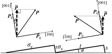
In this paper we propose that steps at the interface, defects which are observed in practically all epitaxial films (due to a small miscut of the substrate by angle ), can be utilized to produce one-dimensional electron gases (1DEG) residing at the step edge. We use a simple model to argue that a step of one unit cell in height alters the polarity of the interface and surface of LAO, since the step edge itself has a net charge of (i.e. a charge line density of , with the step height as in Fig. 1). An equivalent, and more rigorous, picture takes the component perpendicular to the stepped surface of the formal polarization of LAO (Fig. 1), which is precisely (1,1,1) as shown later in the text. The electrostatics of the interface are studied with a simple capacitor plate model, supported with density functional theory (DFT) calculations, that shows an alteration of the interface carrier density with miscut angle. A 1DEG is predicted for small miscut angles when the LAO thickness is just below , the critical thickness for metallicity in the zero miscut system.

We begin with a formal consideration of the polarity of stepped LAO surfaces. We define the miscut angle as tan, where and are the step and terrace distances respectively (see Fig. 1). The steps can be intentionally miscut along a certain direction Brinks et al. (2011); Fix et al. (2011). We consider the [100] case here, but the arguments can be trivially applied to any miscut orientation. Atomic force microscopy (AFM) measurements of epitaxial LAO-STO suggest steps of 1 unit cell in height Brinks et al. (2011); Fix et al. (2011). Neighboring terraces of the surface are then of the same termination (BO2 here), but the step edge may be terminated either AO or BO2 (non-polar vicinal LAO surfaces have been considered in Ref. Stengel, 2011). Perhaps the conceptually simplest picture is to take what has been called “chemical” Bristowe et al. (2009) (or “compositional” Murray and Vanderbilt (2009)) charges, , along the terrace and step edges (Fig. 1 bottom). The total net charge of the surface, , is then cossin. The depends on the step termination: addition if the step and terrace have the same terminations, and subtraction if they have opposite terminations. This result can be confirmed within the framework of the modern theory of polarization King-Smith and Vanderbilt (1993). Taking the formal polarization, , defined by Resta (1994) the position of the ion cores and mapping the electronic wavefunction on to Wannier centers Marzari and Vanderbilt (1997), one finds for cubic LAO along the [111] direction Stengel (2011). The component of this polarization normal to the stepped surface (Fig. 1 top), , is the net surface charge density and precisely the same as the above “chemical” charge. For tetragonal LAO (as in the case of epitaxial thin films), a trivial correction may be applied to the above through a redefinition of .
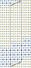
To support this picture, density functional theory (DFT) calculations were performed on two model LAO-STO systems: - superlattices, and - films. and denote the termination of LAO terraces (n - LaO, p - AlO2). Note that in both cases, the steps are created by simply altering one of the supercell vectors - there is no change in stoichiometry through the introduction of steps. The DFT calculations were performed using the Wu-Cohen exchange correlation functional Wu and Cohen (2006) as implemented in the Siesta code Ordejon et al. (1996); Soler et al. (2002). Details of the pseudopotentials and atomic-orbitals basis are given in Ref. Bristowe et al., 2009. We begin with - superlattices (Fig. 2).
Fig. 2 shows the effect of steps on the electronic structure of the - superlattice. The superlattice was constructed from 4.5 unit cells of LAO and 8.5 unit cells of STO stacked along the [001] direction. Steps were introduced by taking a supercell and altering the a supercell vector to a+c (see Fig. 2 left). This produces -type steps along one interface and -type steps along the other while maintaining exactly the same stoichiometry. Fig. 2 shows the case of =3 and =1. In the system without steps (which we call the pristine system) the Ti 3 conduction electrons distribute evenly between the two -type terraces - 0.5 at each interface with a decay through the STO slab (Fig. 2 center), consistent with previous DFT calculations Janicka et al. (2009); Popovic et al. (2008). The inclusion of steps is found to transfer electrons from one interface to the other (Fig. 2 right), accumulating near the -type steps, and depleting near the -type steps, with respect to the pristine system. The total density of electrons transferred is approximately 0.1 (20% of ). This is consistent with the number required to screen the bound charge density of each interface, including the step charges, as predicted by the model. This model system clearly shows a large effect of steps on the interface free electron density and distribution. Note that there has been no change in stoichiometry nor is there any other mechanism suggesting an additional charge transfer.

We now consider a system of more relevance for most experimentally grown systems in reality - - LAO films on STO substrates. The system consists of a slab geometry of LAO unit cells stacked on 5 unit cells of STO along the [001] direction including a 15 Å vacuum layer. A dipole correction was included in the vacuum layer to simulate open-circuit boundary conditions, preventing unphysical macroscopic electric fields due to the asymmetry of the slab and the periodic boundary conditions. The introduction of steps was the same as in the above superlattice case, and chosen such that -type steps reside in the -type terrace, and -type steps reside in the -type terrace. We begin with the case of unit cells, which was found to be beyond the pristine critical thickness within DFT for the onset of metallicity, and then alter the miscut angle, , through varying ( is again fixed at 1 unit cell to resemble that seen in experiments). The total interface free electron density, , is calculated from the projected density of states, which allows one to easily separate free and bound charge due to the existence of a gap. The results are depicted as points in Fig. 3 top, which shows a clear variation of free charge density with miscut angle, going through a maximum (nearly 200% of ) at intermediate angles. Three curves are compared in Fig. 3 top, each with various model approximations, which we discuss next.
To model as a function of we use () Gauss’ Law, , where is the LAO dielectric constant and the LAO internal electric field, and () voltage drop pinning, Bristowe et al. (2009) ( is the STO band gap), obtaining
| (1) |
with cossin the net charge of the stepped interface as discussed earlier, and tantan, the average shortest distance between the stepped plates ( is a geometrical constant depending only on the ratio ). Eq. 1 produces the bold line curve in Fig. 3 top, which is in good agreement with the DFT calculations. Importantly, both the effect of the steps on the net polarization, , and on the effective LAO thickness, , is required to agree with the DFT calculations. Substituting simply the terrace net charge and or the LAO thickness results in disagreement with DFT (dotted and thin lines Fig. 3 top).
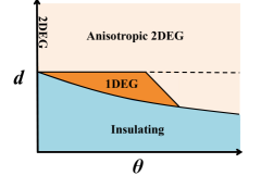
With strong support from the DFT calculations, we explore the model further. Firstly the critical thickness for metallicity as a function of miscut angle, . This is determined from Eq. 1 by setting to zero and rearranging for . A schematic of this transition is shown in Fig. 3 middle, for small , as the curved line separating the insulating phase. The degree of curvature away from horizontal has been exaggerated for clarity. In fact, using the experimental values for and and , it reaches a minimum of about 97% of at . Interestingly, this minimum can be altered through epitaxial strain since the step edge charge density relies on the out-of-plane lattice parameter. Fig. 3 middle shows three other phases above this transition curve - 2DEG, anisotropic 2DEG and 1DEG. Above the pristine critical thickness (horizontal line) an anisotropic 2DEG is predicted at any non-zero miscut angle. This is due to the non-isotropic net charge density of the interface (see later for support from DFT). Between the pristine critical thickness and , and for small , a 1DEG phase is predicted. Introducing steps just below the pristine critical thickness produces carriers in the step edge, to screen the excess interface bound charge. In the limit of very small these are effectively isolated steps. Considering one single step, the excess chemical charge is located around the step for the same reason that the chemical charge associated to the pristine LAO/STO (001) interface is located close to the interface. Since the free carrier charge being transferred is less than the excess chemical charge, the potential well generated by the latter confines the carriers within some width around the step in the direction normal to the step, thereby defining a 1DEG. A phase transition with increasing miscut angle occurs when the 1DEGs, with a finite width, begin to overlap with next neighbor steps. At this point, the 1DEGs are electronically indistinguishable from the anisotropic 2DEG.
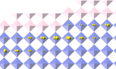
In an attempt to observe the 1DEG, DFT calculations were performed on the film system (see above), with as 2 unit cells, which is lower than the pristine critical thickness, and t=5, s=1. Fig. 3 bottom shows an isosurface of the Ti 3 electron density. The electron density is clearly inhomogeneous, and accumulates near the step edge. The density decays from the step edge in to the terrace, but not to zero. The phase is the anisotropic 2DEG of Fig. 3 middle, below the dotted line. By reducing the miscut angle in the simulation, it should be possible to find the 1DEG, however we are limited to not too small miscut angles due to system size.
Experimental studies of stepped LAO-STO interfaces are few, but we highlight two here. Anisotropic electrical transport has been observed, but explained by anisotropic carrier mobility, not density Brinks et al. (2011). Interestingly, the strongest anisotropy was observed at lowest miscut angles, in disagreement with their step scattering model. Elsewhere, steps were found to affect the carrier mobility and density of the 2DEG Fix et al. (2011). The carrier density was found to decrease with miscut angle, suggesting the possibility of -type step formation.
We hope this work will stimulate the study of stepped surfaces and the search for 1DEGs. Likely candidate systems include; () -type step and terrace terminations, () a theoretical pristine critical thickness of only just beyond an integer number of LAO unit cells, () a maximised curvature of and () a small miscut angle to disconnect the 1DEGs from successive steps, but not too small since the effect of the step polarization is then minimized. In practice this may mean; () surface chemical treatment to alter the step edge termination, () engineering the pristine critical thickness (through for example strain Bristowe et al. (2009); Bark et al. (2011), electric field Thiel et al. (2006); Cen et al. (2008), material Perna et al. (2010) or atmospheric environment if the electronic reconstruction instead occurs via surface chemical redox reactions Cen et al. (2008); Bristowe et al. (2011b)), and () increasing the step bound charge through epitaxial strain, and miscut orientation.
In conclusion we have studied the effects of steps at the LAO-STO interface on the electronic structure. A simple model of polarization and electrostatics is in good agreement with DFT calculations. The model predicts the existence of a 1DEG in the step edge at the interface.
Acknowledgements.
We acknowledge the support of EPSRC and computing resources of CamGRID and Darwin at Cambridge, the Spanish Supercomputer Network and HPC Europa. PBL acknowledges DOE support under FWP 70069.References
- Ohtomo and Hwang (2004) A. Ohtomo and H. Y. Hwang, Nature 427, 423 (2004).
- Brinkman et al. (2007) A. Brinkman, M. Huijben, M. Van Zalk, J. Huijben, U. Zeitler, J. C. Maan, W. G. Van der Wiel, G. Rijnders, D. H. A. Blank, and H. Hilgenkamp, Nat. Mater. 6, 493 (2007).
- Reyren et al. (2007) N. Reyren, S. Thiel, A. D. Caviglia, L. F. Kourkoutis, G. Hammerl, C. Richter, C. W. Schneider, T. Kopp, A.-S. Ruetschi, D. Jaccard, et al., Science 317, 1196 (2007).
- Bert et al. (2011) J. Bert, B. Kalisky, C. Bell, M. Kim, Y. Hikita, H. Hwang, and K. Moler, Nature Physics 7, 767 (2011).
- Li et al. (2011) L. Li, C. Richter, J. Mannhart, and R. Ashoori, Nature Physics 7, 762 (2011).
- Thiel et al. (2006) S. Thiel, G. Hammerl, A. Schmehl, C. W. Schneider, and J. Mannhart, Science 313, 1942 (2006).
- Cen et al. (2008) C. Cen, S. Thiel, G. Hammerl, C. W. Schneider, K. E. Andersen, C. S. Hellberg, J. Mannhart, and J. Levy, Nat. Mater. 7, 298 (2008).
- Xie et al. (2011) Y. Xie, Y. Hikita, C. Bell, and H. Hwang, Arxiv preprint arXiv:1105.3891 (2011).
- Irvin et al. (2010) P. Irvin, Y. Ma, D. Bogorin, C. Cen, C. Bark, C. Folkman, C. Eom, and J. Levy, Nature Photonics 4, 849 (2010).
- Nakagawa et al. (2006) N. Nakagawa, H. Hwang, and D. Muller, Nat. Mater. 5, 204 (2006).
- Schlom and Mannhart (2011) D. Schlom and J. Mannhart, Nat. Mater. 10, 168 (2011).
- Stengel and Vanderbilt (2009) M. Stengel and D. Vanderbilt, Phys. Rev. B 80, 241103 (2009).
- Bristowe et al. (2011a) N. Bristowe, P. Littlewood, and E. Artacho, J. Phys.: Condens. Matter 23, 081001 (2011a).
- Vanderbilt and King-Smith (1993) D. Vanderbilt and R. King-Smith, Phys. Rev. B 48, 4442 (1993).
- Bristowe et al. (2011b) N. C. Bristowe, P. B. Littlewood, and E. Artacho, Phys. Rev. B 83, 205405 (2011b).
- Brinks et al. (2011) P. Brinks, W. Siemons, J. Kleibeuker, G. Koster, G. Rijnders, and M. Huijben, Appl. Phys. Lett. 98, 242904 (2011).
- Fix et al. (2011) T. Fix, F. Schoofs, Z. Bi, A. Chen, H. Wang, J. MacManus-Driscoll, and M. Blamire, Appl. Phys. Lett. 99, 022103 (2011).
- Stengel (2011) M. Stengel, Phys. Rev. B 84, 205432 (2011).
- Bristowe et al. (2009) N. C. Bristowe, E. Artacho, and P. B. Littlewood, Phys. Rev. B 80, 045425 (2009).
- Murray and Vanderbilt (2009) É. Murray and D. Vanderbilt, Phys. Rev. B 79, 100102 (2009).
- King-Smith and Vanderbilt (1993) R. D. King-Smith and D. Vanderbilt, Phys. Rev. B 47, 1651 (1993).
- Resta (1994) R. Resta, Rev. Mod. Phys. 66, 899 (1994).
- Marzari and Vanderbilt (1997) N. Marzari and D. Vanderbilt, Phys. Rev. B 56, 12847 (1997).
- Wu and Cohen (2006) Z. Wu and R. Cohen, Phys. Rev. B 73, 235116 (2006).
- Ordejon et al. (1996) P. Ordejon, E. Artacho, and J. M. Soler, Phys. Rev. B 53, 10441 (1996).
- Soler et al. (2002) J. Soler, E. Artacho, J. Gale, A. Garcia, J. Junquera, P. Ordejon, and D. Sanchez-Portal, J. Phys.: Condens. Matter 14, 2745 (2002).
- Janicka et al. (2009) K. Janicka, J. Velev, and E. Tsymbal, Phys. Rev. Lett. 102, 106803 (2009).
- Popovic et al. (2008) Z. S. Popovic, S. Satpathy, and R. M. Martin, Phys. Rev. Lett. 101, 256801 (2008).
- Bark et al. (2011) C. Bark, D. Felker, Y. Wang, Y. Zhang, H. Jang, C. Folkman, J. Park, S. Baek, H. Zhou, D. Fong, et al., Proceedings of the National Academy of Sciences 108, 4720 (2011).
- Perna et al. (2010) P. Perna, D. Maccariello, M. Radovic, U. Scotti di Uccio, I. Pallecchi, M. Codda, D. Marre, C. Cantoni, J. Gazquez, M. Varela, et al., Appl. Phys. Lett. 97, 152111 (2010).