Long range spin supercurrents in ferromagnetic CrO2 using a multilayer contact structure
Abstract
We report measurements of long ranged supercurrents through ferromagnetic and fully spin-polarized CrO2 deposited on TiO2 substrates. In earlier work, we found supercurrents in films grown on sapphire but not on TiO2. Here we employed a special contact arrangement, consisting of a Ni/Cu sandwich between the film and the superconducting amorphous Mo70Ge30 electrodes. The distance between the contacts was almost a micrometer, and we find the critical current density to be significantly higher than found in the films deposited on sapphire. We argue this is due to spin mixing in the Ni/Cu/CrO2 layer structure, which is helpful in the generation of the odd-frequency spin triplet correlations needed to carry the supercurrent.
Conventional spin-singlet Cooper pairs from a superconductor (S) dephase over a
coherence length (dirty limit) in a ferromagnet
(F) under the influence of its exchange field (and the diffusion
constant in the F-metal). Even for weak ferromagnets, is only a few nm.
Such dephasing would not occur with equal-spin triplet Cooper pairs, leading to
a long range proximity (LRP) effect in the ferromagnet. It was predicted that
triplet correlations can be induced at an S/F interface when is
inhomogeneous Bergeret01 ; Kadigrobov01 ; Eschrig08 , for instance from
domain walls or unaligned magnetic moments. This should also allow a Josephson
current in an S/F/S geometry. To observe this, both interfaces are required to
show similar inhomogeneities Houzet07 as for instance in an
S/F1/F/F2/S trilayer in which the magnetizations of the F1,
F2 layers are non-collinear with the central F layer.
Early work on CrO2 Keizer06 and Holmium Sosnin06 gave the
first indications for such LRP effects in ferromagnets. In the first case, a
supercurrent was measured in devices where superconducting electrodes of NbTiN
with separations up to 1 m were placed on unstructured 100 nm thick films
of CrO2 (a half metallic ferromagnet or HMF) which were grown on TiO2
substrates. In the second case, the LRP effect was observed in ferromagnetic Ho
wires of lengths up to 150 nm using an Andreev interferometer geometry. More
recently, LRP effect were reported using Josephson junctions where a Co central
layer was used in combination with PdNi, CuNi or Ni layers
Khaire10 ; Khasawneh11 ; and where a Co layer was used together with Ho
layers to provide magnetic inhomogeneity Robinson10 . Signatures of LRP
effect were also observed with the Heusler Compound Cu2MnAl
Sprungmann10 and in Co nanowires Wang10 . At the same time, the
observation of supercurrents over a length of 700 nm through
CrO2 deposited on sapphire substrates was reported Anwar10 ; Anwar11 .
The experiments with Co junctions were up to Co thicknesses of 50 nm. Since Co
is not fully spin polarized the triplet decay is mainly set by the spin
diffusion length, and can be expected to be of the order of 100 nm. That makes
the CrO2 case with its significantly larger decay length of special
interest, but in the previous experiments the reproducibility was an issue. In
particular, it was not clear where the inhomogeneous magnetization resides
which is needed for the triplet generation. Also, in our previous work we did
not succeed in finding supercurrents in films deposited on TiO2. Here we
report on observing long ranged supercurrents in CrO2 grown on TiO2,
using 2 nm Ni as an extra layer in the contact geometry to induce an artificial
magnetic inhomogeneity, and 5 nm Cu to magnetically decouple the Ni and the
CrO2. We find much stronger supercurrents than in the case of sapphire,
indicating that with the Ni/Cu sandwich we have a good generator for triplet
Cooper pairs.
The devices were fabricated in a lateral geometry using 60 nm thick
a-Mo70Ge30 superconducting contacts (transition temperature =
6 K) deposited on unstructured 100 nm thick CrO2 films grown on TiO2
substrates. We made the devices through a lift-off mask using a bilayer resist.
Ar-ion etching was applied immediately prior to deposition, in order to remove
the Cr2O3 on the film surface, and the Cu/Ni/Mo70Ge30
sandwiches were sputtered in situ. Two junctions were made on each
sample, perpendicular to each other, and both junctions were measured
independently. More details can be found in
Refs.Anwar10 ; Anwar11
A supercurrent was measured successfully in three devices out of five, named
AT, BT and CT. On AT (30 m wide leads) both junctions showed a
supercurrent. We call them AT-a (600 nm gap) and AT-b (800 nm gap).
Samples BT and CT were prepared with 5 m wide leads, in order to
lower the absolute value of the currents, and a gap of 700 nm. Here only one
junction was showing a measurable critical current on each sample. Sample CT
was measured in two different cryostats, one with extra filtering to minimize
to amplifier contribution to the data in the zero-voltage branch. A drawback
still is the limited lifetime of the samples. The supercurrent disappears after
a few cool-downs, possibly due to the effect of thermal cycling on the films.
For sample AT, the resistance as function of temperature is given in
Fig. 1a and shows a sharp down-jump at . For junction
BT (Fig. 1b), shows a small dip at 6 K, followed by
an up-jump, a flat part, and then a slow decrease. For junction CT the
behavior is similar but with a larger up-jump to 0.7 , similar to our
sapphire-based devices Anwar11 .
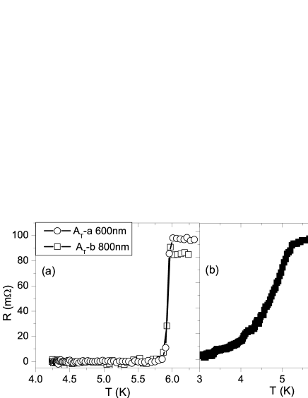
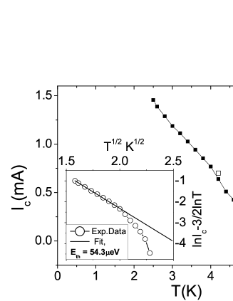
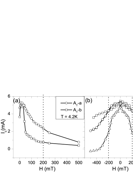
Figure 2a shows an - characteristic for sample AT-b, measured at 4.2 K. There is a zero-resistance branch up to a well-defined current of about 3 mA at which a finite voltage develops. On larger scales a bend in the curve is seen, followed by another transition at 15 mA to Ohmic behavior with RN=100 m. Figure 2b shows - data measured on sample BT at 3 K. The value for is 1.2 mA, and the resistive branch has a value of 80 m, in very reasonable agreement with the normal state resistance. The residual resistance below is a few m. Sample CT was first measured at 4.2 K in a cryostat with well-filtered leads. Here, the - characteristic showed sharp switching and some hysteretic behavior, with of the order of 0.5 mA. The residual resistance below is 3 m. was defined by a 1 V criterion and measured for junction BT and CT in the temperature range of 2.5 K to 6 K. As shown in Fig. 3 for sample BT the behavior is almost linear. For sample AT we first measured the field dependence of at 4.2 K, but we did not measure because the supercurrent disappeared after the third cool-down. The measurement on sample CT is also shown in Fig. 3. In a subsequent measurement, had gone down to 70 , illustrating the fragility of the sample, but also showed a linear increase. Figure 4a illustrates the effect of a magnetic field on at 4.2 K for both junctions AT-a and AT-b, with in the plane of the junction and . It shows that in the case of AT-a is quite sensitive to , with an initial fast decrease below 60 mT, but less so in the case of AT-b. Figure 4b presents at 3 K for junction BT in three different configurations, in-plane and , and out-of-plane. Here the field-in-plane data show a relatively slow decrease, while the field-out-of-plane data show a small sharp peak, followed by a shoulder around 100 mT. Neither for AT-a,b nor for BT there is evidence for a Fraunhofer pattern.

The claim from the measurements is that large supercurrents are now flowing
through the CrO2 bridge. In discussing these results we address the
following issues. We compare the residual resistance in the supercurrent
measurements with the normal state resistance of the bridge; we discuss the
possibility of depairing currents in the superconducting leads; a Thouless
analysis is performed; and we discuss the effects of applying a magnetic
field.
The ’s measured here can be compared with our previous measurements
Anwar10 ; Anwar11 on sapphire-based junctions. The current density at
4.2 K, (d 100 nm, junction width 30 m and 5 m,
current 3 mA and 0.5 mA respectively) is of the order of 1
109 A/m2 for AT, BT, as well as CT. In all cases, it is 100
times larger than that of sapphire-based junctions, and of similar magnitude as
in the earlier observations of Keizer et al. Keizer06 . This
suggests that a uniform spin active interface is present at the interface, due
to the additional 2 nm Ni layer.
An important question is whether the characteristics such as shown in
Fig. 2 are truly from the CrO2 bridge, and not just the
superconducting contacts. For this we take another look at the normal
resistance of the bridge. Taking =10 cm, a film
thickness of 100 nm, a bridge width of 5 m, and a junction length of
700 nm, comes out to be 140 m (25 m for the 30 m
wide contacts). This is significantly higher than what is measured in the
zero-voltage branch of the - characteristics, where it is not more than a
few m. Note that the measured resistance above is higher than the
above estimate. This is because, when the superconducting leads become normal,
the geometry of the sample is a very different one, with both high resistance
MoGe and low-resistance CrO2 contributing.
Another issue is how close comes to the depairing current of the
superconducting leads. For the sapphire-based junctions with their low
values this was not relevant. The value for of a-MoGe is about 4
1010 A/m2 at 4.2 K Rusanov04 . Taking into account that
the thickness of the lead (40 nm) is smaller than that of the bridge, the
current density in the lead at the measured for all junctions is about
A/m2, still an order of magnitude smaller than .
This probably explains, however, the second transition seen in Fig.2a,
which takes place at a 5 times higher current density.
Although is quite linear, the Thouless energy of the junction can be
estimated from a plot of (ln()-(3/2 ln(T)) versus (see inset of
Fig.3). For junction BT we find Eth = 54 eV, not much
different from that of sapphire based junctions Anwar10 ; Anwar11 . From
ETh we can estimate at 4.2 K using theoretical results for a long
junction dubos01 . For (k/ETh) 7.6, we find from
Ref.dubos01 that 54 V, which
with = 60 m leads to = 0.9 mA , quite close to the measured
value.
The magnetic field effects are complicated. For the junctions
AT-a,b are more sensitive to the field than BT. For junctions AT-a,b
the first sharp decrease at 60 mT might correspond to the first flux quantum,
which is a reasonable value according to the dimensions of the junctions, but
no such behavior is seen for BT. The suppression of is stronger than
in the earlier work. Taking a 200 mT field as a reference point, the
suppression is over 70% for AT, and still almost 30% for BT, compared
to 10% in the sapphire-based junctions. This points to a diminishing
effectiveness of the Ni/Cu layer, although it might be argued that the effect
should be even stronger: in 200 mT both the CrO2 and Ni magnetization should
be saturated and aligned, removing a possible source of magnetic inhomogeneity.
Instead, the supercurrents were not even quenched in 500 mT. It suggests that
there is a residual magnetic inhomogeneity residing in the Ni/Cu/CrO2
sandwich, which is not removed by the magnetic field. This needs further study.
In conclusion, a Ni/Cu sandwich on top of ferromagnetic CrO2 deposited on
TiO2 substrates leads to strong supercurrents over a distance of almost
1 m. The Ni/Cu sandwich appears to furnish spin mixing and triplet
generation similar to what was found in Co-based junctions.
This work is part of the research program of the Stichting F.O.M.,
which is financially supported by NWO. M.S.A. acknowledges the financial
support of the Higher Education Commission (HEC) Pakistan.
References
- (1) F. S. Bergeret, A. F. Volkov and K. B. Efetov, Phys. Rev. Lett. 86, 4096 (2001).
- (2) A. Kadigrobov, R. I. Shekhter and M. Jonson, Europhys. Lett. 54, 394 (2001).
- (3) M. Eschrig and T. L fwander, Nat. Phys. 4, 138 (2008).
- (4) M. Houzet and A. I. Buzdin, Phys. Rev. B 76, 060504 (2007).
- (5) R. S. Keizer, S. T. B. Gönnenwein, T.M. Klapwijk, G. Miao, G. Xiao and A. Gupta, Nature 439, 825 (2006).
- (6) I. Sosnin, H. Cho, V. T. Petrashov and A. F. Volkov, Phys. Rev. Lett. 96, 157002 (2006).
- (7) T. S. Khaire, M. A. Khasawneh , W.P. Pratt Jr and N. O. Birge, Phys. Rev. Lett. 104, 137002 (2010).
- (8) M. A. Khasawneh, T. S. Khaire, C. Klose, W. P. Pratt Jr and N. O. Birge, Superc. Sci. Technol. 24, 024005 (2011).
- (9) J. W. A. Robinson, J. D. S. Witt and M. G. Blamire, Science 329, 59 (2010).
- (10) J. W. A. Robinson, S. Piano, G. Burnell, C. Bell, and M. G. Blamire, Phys. Rev. Lett. 97, 177003 (2006).
- (11) M. S. Anwar, F. Czeschka, M. Hesselberth, M. Porcu, and J. Aarts, Phys. Rev. B 82, 100501(R) (2010).
- (12) M. S. Anwar, and J. Aarts, Superc. Sci. Technol. 24, 024016 (2011).
- (13) D. Sprungmann, K. Westerholt, H. Zabel, M. Weides, and H. Kohlstedt, Phys. Rev. B 82, 060505(R) (2010).
- (14) J. Wang, M. Singh, M. Tian, N. Kumar, B. Liu, C. Shi, J. K. Jain, N. Samarth, T. E. Mallouk and M. H. W. Chan, Nat. Phys. 6, 389 (2010).
- (15) A. Yu. Rusanov, M. B. S. Hesselberth, and J. Aarts, Phys. Rev. B 70, 024510 (2004).
- (16) P. Dubos, H. Courtois, B. Pannetier, F. K. Wilhelm, A. D. Zaikin, and G. Schön, Phys. Rev. B 63, 064502 (2001).