The Optical Excitation of Zigzag Carbon Nanotubes with Photons Guided in Nanofibers
Abstract
We consider the excitation of electrons in semiconducting carbon nanotubes by photons from the evanescent field created by a subwavelength-diameter optical fiber. The strongly changing evanescent field of such nanofibers requires dropping the dipole approximation. We show that this leads to novel effects, especially a high dependence of the photon absorption on the relative orientation and geometry of the nanotube-nanofiber setup in the optical and near infrared domain. In particular, we calculate photon absorption probabilities for a straight nanotube and nanofiber depending on their relative angle. Nanotubes orthogonal to the fiber are found to perform much better than parallel nanotubes when they are short. As the nanotube gets longer the absorption of parallel nanotubes is found to exceed the orthogonal nanotubes and approach 100% for extremely long nanotubes. In addition, we show that if the nanotube is wrapped around the fiber in an appropriate way the absorption is enhanced. We find that optical and near infrared photons could be converted to excitations with efficiencies that may exceed 90%. This may provide opportunities for future photodetectors and we discuss possible setups.
pacs:
78.67.Ch, 78.40.Ri, 73.22.-f, 78.30.NaI Introduction
The unique physical properties of carbon nanotubes and the flexibility they provide in selecting their characteristics offers great potential for nanotechnology Charlier et al. (2007); Ando (2005); Saito et al. (1998). Carbon nanotubes can be either semi-conducting or metallic, depending on their diameter and helical configuration. They typically have nanometer sized diameters and a length of a few microns, although centimetre long nanotubes have been produced recently Wang et al. (2009). This makes them ideal 1D systems that possess a ballistic conducting channel White and Todorov (1998), no backward scattering, and energy levels that can be adjusted with external fields Klinovaja et al. (2011); Kim and Chang (2001); Pacheco et al. (2005). Superconductivity has also been observed in multi-walled carbon nanotubes and single carbon nanotubes have exhibited a superconducting proximity effect Takesue et al. (2006); Noffsinger and Cohen (2011); Kasumov et al. (1999); Morpurgo et al. (1999). Their applications range from extremely strong fibers and organic electronics Uchida and Okada (2009) to electrochemical sensors Snow et al. (2005); Tang et al. (2006) and photon detectors Freitag et al. (2003).
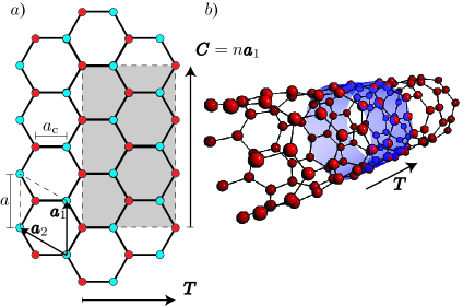
Carbon nanotubes are a form of carbon formed by rolling up a sheet of graphene into a cylindrical tube. An illustration of this is given in Fig. 1. Here we focus on the optical properties of carbon nanotubes. For a straight nanotube, inside a weak uniform classical plane wave field, these properties have been extensively studied Spataru et al. (2004); Jiang et al. (2004); Motavas et al. (2010); Zarifi and Pedersen (2009); Goupalov et al. (2010); Goupalov (2005); Berciaud et al. (2010); Takagi and Okada (2009); Zarifi and Pedersen (2006); Malić et al. (2006); Saito et al. (2004). Their quasi one-dimensionality means that their density of states exhibit Van Hove singularities and these contribute to strong optical absorption peaks. However, these results apply the dipole approximation, where it is assumed that the field does not vary along the nanotube’s length. We extend this treatment by allowing for the spatial dependence of the field. This situation is particularly relevant when the electrons are delocalized in a tightly-confined field, such that the field varies greatly over a few hundred nanometres. The degree to which the electrons are delocalized is a topic of ongoing research and various studies have been done on the coherence length in nanotubes. Their results range from nm to several microns suggesting that the spatial field dependence is certainly important for confined fields and may also be relevant for plane waves Miyauchi et al. (2009); Roche et al. (2005a); Tans et al. (1997); Roche et al. (2005b); Perebeinos et al. (2005).
The systems we are primarily interested in are subwavelength-diameter optical fibers coupled to carbon nanotubes. The electrical field of a nanofiber is tightly confined and primarily exists outside of the fiber, in a large evanescent field Bures and Ghosh (1999). Due to the presence of a strong field in a relativity small volume, these nanofibers are ideal candidates to achieve a high optical absorption in atomic systems. For example, their interaction with atom-arrays has been studied Le Kien et al. (2005); Sagué et al. (2007); Vetsch et al. (2010). However, in contrast to such atom-fiber systems, the dipole approximation can not be applied in the case of nanotubes since the optical field typically changes rapidly along a nanotube’s length. In this paper we calculate the (internal) quantum efficiency, i.e. the probability that a nanotube, placed inside the evanescent field of a nanofiber, absorbs a photon. Calculations for the external quantum efficiency, i.e. the efficiency for detecting the excitation with the photocurrent, are beyond the scope of this paper. However, it should be noted that important effects that could aid in this procedure, such as the avalanche effect, have been observed in carbon nanotubes Liao et al. (2008). We focus specifically on the example of zigzag nanotubes (see Fig. 1) because they can be direct semiconductors. However, our results are still representative of other semiconducting nanotube types such as chiral nanotubes. We find that the absorption is extremely dependent on the nanotube’s orientation. These results are highly relevant for the interface between any future nanoscale photonics and carbon nanotubes. If the absorption process is coherent the system may also be suitable as a quantum memory, that maps a photonic quantum state on to a coherent excitation of the nanotube.
We will be using the band-to-band tight binding transition model for the carbon nanotube. This has proven itself to be very effective in determining the basic optical properties of nanotubes but does not include effects due to excitons Dresselhaus et al. (2007) and electron-electron interactions Bunder and Hill (2009). Such effects give measurable corrections and there have been a few studies considering the exciton absorption strength Spataru et al. (2004); Mohite et al. (2008); Berciaud et al. (2010); Ichida et al. (1999). Nevertheless, the band-to-band model is suitable to determine the main contributions to optical absorption.
This paper is organized as follows. We begin by giving an overview of nanotube properties and the calculation of their band structure in Sec. II. Based on this we then evaluate the photon absorption by zigzag carbon nanotubes in Sec. III. In the setups considered in this paper the nanotubes experience fields that change strongly along their length, i.e. to calculate photon absorption we can not rely on the dipole approximation. We obtain general expressions for the absorption probability which are then applied to cylindrical vacuum cladded silica nanofibers in Sec. IV, and discuss different geometrical setups of nanofiber and nanotube. Possible photodetectors that use these setups are then presented in Sec. V. Finally, in Sec. VI, we summarize our results.
II The Tight-binding Model for the Carbon Nanotube
Here we will review the basic properties of carbon nanotubes for completeness and layout the notation that we use in later sections. A single walled carbon nanotube (SWCNT) can be thought of as a sheet of graphene wrapped into a tube, so we will start by describing the tight-binding model of graphene Abergel et al. (2010). Graphene is a regular 2D hexagonal Bravais lattice of carbon atoms and its structure is shown in Fig. 1. We label the unit vectors of the graphene lattice and . The length of these vectors is the lattice constant which is related to the distance between neighboring carbon atoms, , by nm. Within each unit cell there are two carbon atoms, that we label to form the A and B sublattices. We can then define the unit vectors of the reciprocal lattice as and , with . The first Brillouin zone given by these is also hexagonal. It has a selection of points with high-symmetry; one at the center, the midpoints of the hexagonal edges and two inequivalent types of corners.
The well-established tight-binding model assumes that the electrons are tightly bound to the individual carbon atoms and the localized atomic orbitals are used as a basis for expanding the wavefunction. We consider orbitals that contribute to states that lie within an optical range of energies around the Fermi level. These are the states that give the main contributions to the optical properties of the nanotube. Every carbon atom has four valence orbitals (2s, 2, 2 and 2) that could lie in this energy range. For 2D graphene the (s, , ) orbitals combine to form hybridized orbitals. These give the strong covalent bonds; primarily responsible for the binding energy and elastic properties of the nanotubes. In the tight-binding model they result in and bands. However, their energy levels are far away from the Fermi level and hence they do not play a key role in the optical properties that we are interested in. That role is played by delocalized and bands that are formed from the orbitals Charlier et al. (2007). Hence, we can ignore the electrons and restrict the tight-binding model to the electrons. The Hamiltonian for this system is
| (1) |
where is the hopping amplitude and refers to nearest neighbors. Here, and are the creation operators for electrons in sublattice A and B, respectively. In this Hamiltonian we have removed the constant energy contribution that corresponds to the Fermi level. We expand the wavefunction in terms of orbitals at every atom site and split this expression into two parts; one for each sublattice. The wavefunction for each state is then
| (2) | ||||
| (3) |
with , labeling the atom locations in sublattice A and B, respectively. The individual orbitals are given by the normalized wavefunctions and each one has a coefficient, represented with and . By using translational symmetry we can represent this as
| (4) |
where the Bloch functions, and , are
| (5) | ||||
| (6) |
Here is the number of unit cells in the graphene sheet. These bloch functions have the coefficients and . The states are labeled by their crystal momentum vector . We now solve the time-independent single-particle Schrödinger equation
| (7) |
We define the quantity
| (8) |
where are vectors from an atom in the A sublattice to its neighboring atoms in the B lattice. This gives us the following quantities
| (9) |
Now the variational Schrödinger equation in matrix form is
| (10) |
The above matrix equation can be solved to give the energy of each state as
| (11) |
where
| (12) |
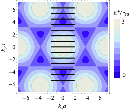
A typical value for is eV such that the tight-binding model corresponds with experiments Grüneis et al. (2003); Saito et al. (2000, 1998). We will keep in the equations but for all plots and numerical calculations we assume that , i.e. there is no orbital overlap. In Fig. 2 this 2D dispersion relation is plotted as a contour. In Eq. (11) the signs refer to the two relevant bands, the conduction band and the valence band. The coefficients are found to be
| (13) | ||||
| (14) | ||||
| (15) | ||||
| (16) |
Now we know the relevant band structure of graphene and their wavefunctions, we need to obtain the energy states of the nanotubes. To do this we use the zone-folding approximation. This assumes the nanotube bands are the same as graphene but with limited , due to the 1D nature of a carbon nanotube. There are a variety of ways available to wrap the sheet up into a nanotube, each of which result in very different properties. The nanotubes are characterized by a vector in the graphene plane that corresponds to the circumference of the nanotube and is called the chiral vector (see Fig. 1). It gives the relative position of two graphene atoms that become ‘identical’ when the graphene is rolled into a nanotube. We will use these parameters in the standard form to label each type of nanotube. This immediately defines some basic geometric properties such as the tube’s circumference and radius .
We also define the translational vector, perpendicular to , that corresponds to the direction along the tube, . Using the greatest common divisor (gcd), we define , and . The two vectors, and , define the unit cell of the nanotube. Within each nanotube unit cell there are graphene unit cells and, hence, carbon atoms. In a nanotube of length there are nanotube unit cells. For the nanotube’s reciprocal lattice we define and such that and . These give the allowed vectors in the SWCNT’s Brillouin zone to be a set of 1D ‘cutting lines’ with values
| (17) |
with and . It is the periodic boundary condition along the circumferential direction of the tube that causes the wave vector to become quantized and each discrete cutting line is labeled by the azimuthal quantum number . For short nanotubes the wave vectors are also quantized along the nanotube’s length causing discrete energy levels to be formed Nikolaev et al. (2009). These discrete values have , for an integer . Local effects also occur in short nanotubes, such as a sharp spike in the density of states (DOS), caused by defects at the caps. Such effects will be ignored here. Typically, the nanotube is assumed to be of infinite length, allowing continuous values of the wave vector along the nanotube axis. This causes possible wave vectors to lie in ‘subbands’. The subbands can cut through the fermi points of graphene causing the tube to become metallic. This can be shown to be the case for nanotubes of the type , where is a multiple of three. If this is not the case there is a nonzero band gap and the nanotube is semiconducting. Here we consider ‘zigzag’ semiconducting nanotubes of the form , with not a multiple of three. The discrete wave vectors are then
| (18) |
with and
| (19) |
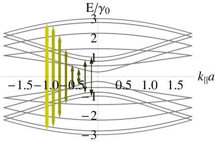
The momentum vectors associated with these subbands are highlighted in Fig. 2 for a (7,0) nanotube. For zigzag nanotubes corresponds to and corresponds to . It should be noted that subbands and both have the same energy and this degeneracy is referred to as the ‘valley’ degeneracy. Combined with the two electron spins this gives a degeneracy of four for each energy value, except for and that only have spin degeneracy. The energy of the subbands is
| (20) |
These are plotted for a (7,0) nanotube in Fig. 3, which has a bandgap of eV.
III The Optical Absorption of Carbon Nanotubes
The Hamiltonian of a nanotube interacting with an electromagnetic field is , with
| (21) |
being the interaction term and representing the field Hamiltonian. Here, we define as the magnitude of the electron charge and are using SI units. Each field mode is characterized by its angular frequency and further parameters, which define the mode’s polarization and propagation direction. The field vector potential operator is
| (22) |
We will consider the initial and final state of field to be a coherent monochromatic state , with an angular frequency of and a mean photon flux of photons per unit time. This state satisfies the equation , with and being the field mode’s destruction operator Blow et al. (1990). This allows us to give
| (23) | ||||
| (24) |
Using time-dependent perturbation theory we find that, after time , the initial state of the nanotube and field, , is in the state with probability
| (25) |
which is Fermi’s Golden Rule. The transition rate for each electron in the state with energy to each state with energy can be expressed as
| (26) |
To calculate the optical absorption of a carbon nanotube of length , the interaction term, , needs to be found with spatially changing field. Here we are assuming that the state is coherent over the entire length of the nanotube. To calculate we define
| (27) | ||||
| (28) |
with summing over the three vectors pointing from an atom in the A sublattice to its neighboring three B lattice atoms. We will furthermore use the matrix element, , with being the vector between two neighboring atoms such that the z-axis is aligned along . The value we will later use for this is given by Zarifi and Pedersen (2006)
| (29) |
Each of the unit cells in the nanotube extends over a distance of nm along the nanotube and approximately a nanometre across. This is much smaller than the light’s wavelength and spatial variations. Therefore, we can assume that the electromagnetic field is constant across each of the nanotube’s unit cells. There are of these unit cells along the nanotube’s length and in each one, labeled by an integer , the field is given by .
An expression for can then be calculated and simplified into the form (see Appendix A)
| (30) | ||||
| (31) |
where
| (32) |
and are given in Appendix A.
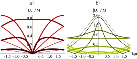
This result coincides with that of Ref. Jiang et al. (2004) when is the same for all . In Eq. (31) the gives the selection rules for possible transitions between bands and . In particular is negligible if and for the other components of to contribute we require . For a uniform field across the nanotube these give the possible transitions for a field polarized parallel and perpendicular to the nanotube, respectively. In Fig. 4 we have plotted , and in Fig. 5 is plotted. These expressions correspond to direct transitions, i.e with , which is an approximation of momentum conservation and will be discussed later in this section.
Although the values of and show a transition, the induced local field creates a depolarization effect Tasaki et al. (1998); Ajiki and Ando (1994); Islam et al. (2004) that reduces and to give a negligible contribution to the absorption. This allows us to focus on the term and simplify to
| (33) |
with denoting the length along the nanotube. This also restricts the transitions to those with .
It is the line integral in Eq. (33) that is responsible for momentum conservation in the system. The photon momentum is much smaller than the crystal momentum and typically only direct transitions are considered, i.e. . Here we will make this assumption, however the change in momentum can not be completely neglected since any change can make a major difference to the line integral in Eq. (33). This is especially true when the field oscillates along the nanotube. The energy of a direct transition is given by . Since , when , we will make this substitution and further simplify to give
| (34) |
We define to be the field potential along the nanotube and use the discrete momentum values, and , with integers and . The line integral can then be expressed as
| (35) | ||||
| (36) | ||||
| (37) |
This expression is simply the coefficient in the Fourier series for . Since the photon momentum is very small in comparison to the crystal momentum the only relevant coefficients will have very small values of relative to . Every electron transition in the nanotube then needs to be considered to calculate the overall absorption rate. This leads to a length dependence on the absorption. We initially consider discrete states and corresponding values. The transition rate given by Eq. (26) is summed over all possible initial and final states to give
| (38) |
In this equation refer to the degeneracy of the initial state. For any value of the sum over causes to take all of the low values that are relevant. This sum is also independent of and allows us to define , which can be rewritten using Parseval’s theorem to be
| (39) |
The total absorption rate is then
| (40) | ||||
| (41) |
where we define
| (42) |
The field was defined to be a coherent state with a photon flux given by photons per unit time. We divide the transition rate, given in Eq. (41), by this flux to obtain an estimate for the probability of one photon exciting a single electron. This expression gives a probability that increases linearly with nanotube length. This is certainly suitable up to the coherence length, , however not for long nanotubes. So far we have considered the length of the nanotube to be smaller than the coherence length. For long nanotubes we can consider the whole nanotube to be composed of coherent segments. This leads to an exponential increase in the absorption with the nanotube length. Here, to calculate this quantity we find the probability of not exciting any electrons, which is the product of for each segment. Hence, the probability of exciting a single electron, in a nanotube of length , with each photon can be estimated by the expression
| (43) |
Note that this expression is actually independent of the coherence length.
Broadening effects can be included in this by substituting the Dirac delta function, from Eq. (42) with a Lorentzian function,
| (44) |
that has a broadening parameter, . This parameter can include the broadening due to multiple effects, including the electronic state’s decay. In carbon nanotubes the state decay occurs on a picosecond time scale Lauret et al. (2003). If we take a range of ps to ps the required broadening ranges from eV to eV. In order to compare our results with previous work Zarifi and Pedersen (2006); Lin (2000) we will choose in the following to use a parameter of eV.
So far we have assumed the light to be in a pure state consisting of one specific wavelength. We expect to have a range of wavelengths present and to deal with this we assume the light is in a probabilistic mixture of coherent beams, each with a photon flux . These are weighted by a lineshape , satisfying . The light’s state is then and the expected absorption probability is
| (45) |
In the following we take to be a uniform lineshape between two energy values. This is equivalent to taking to be the average transition probability over a range of energies.
IV Optical Nanofiber Photon Absorption into a Carbon Nanotube
We now extend the calculation for the absorption around optical fibers and particularly nanofibers Tong et al. (2003); Tong and Mazur (2008). A review of these subwavelength diameter waveguides can be found in Refs. Brambilla et al. (2004); Tong (2010); Tong et al. (2004). They are made of a silica core and have diameters as small as nm. For fibers of this size a high proportion of the light field exists outside of the fiber’s core. This means the field is easily accessible and we consider positioning the carbon nanotube near the nanofiber. The use of fibers allows the interaction to be enhanced due to the transverse confinement of the field. Altering the nanofibers properties also allows us to tailor the field. Fibers with a smaller diameter have a larger evanescent field but also suffer from higher losses. We will consider a cylindrical nanofiber core with a radius of and cladding provided by the vacuum, with refractive index . The refractive index of the silica core is and the material absorption of the silica is negligible over the short distances being considered. Silica core fibers with subwavelength diameter are single mode fibers, i.e. the only mode present is the HE fundamental mode (see Ref. Tong et al. (2004) for a general single mode condition). In the following we will adopt a scheme used in Refs. Le Kien et al. (2005); Blow et al. (1990) to quantize the field. The field potential operator for the nanofiber’s fundamental mode is then
| (46) |
This is given in terms of cylindrical coordinates, with being the coordinate along the fiber and the azimuthal angle. The light’s angular frequency is . Its propagation direction is labeled with and refers to the longitudinal propagation constant. We find the value of by numerically solving the fiber eigenvalue equation (see Eq. (63) in Appendix B). The derivative in Eq. (46), , is taken with respect to , and are the photon annihilation operators, with characterizing the separate modes. Furthermore, are the electric field profiles of the guided mode that can be found by solving Maxwell’s equations Snyder and Love (1983); Le Kien et al. (2005) and gives a normalization factor. The expressions for the mode profiles and are given in Appendix B. The polarization can be right or left circular labeled by . For a single mode of monochromatic coherent light with we have
| (47) |
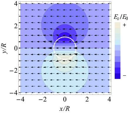
Fig. 6 provides a slice of the classical field at one instant in time. This field can be seen to extend far away from the nanofiber and vary dramatically with position.
This contrasts with the simpler case, that has previously been studied, of a plane linearly polarized light beam that is given by
| (48) |
across the whole nanotube, where the beam has a finite cross-sectional area of . This gives
| (49) |
For fibers larger than nm in diameter the photon losses are small and can be ignored over short distances. In our calculations we will use nanofibers of diameter nm. Furthermore, we will focus on the forward propagation and right polarized guided modes, i.e. . All other modes are related to our results by symmetry. The value of is then highly dependent on the way the nanotube is orientated relative to the nanofiber and can be calculated to be
| (50) |
Since the field strength drops off exponentially the highest value for the coupling will be achieved by having the nanotube as close as possible to the fiber. In our examples, the distance between the nanotube’s center and the surface of the nanofiber is chosen to be nm. The nanotubes we consider always have a radius less than nm so this distance avoids any contact. There are two orientations we will consider. The first is that of a straight nanotube, of length , oriented at an angle relative to the nanofiber which includes parallel and perpendicular orientations as illustrated in Fig. 7.
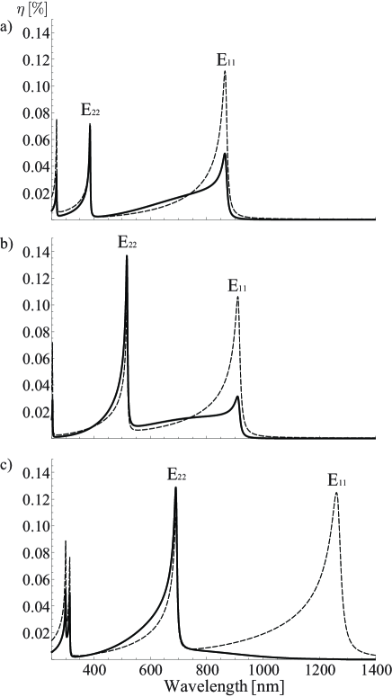
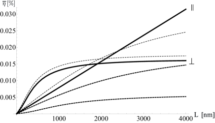
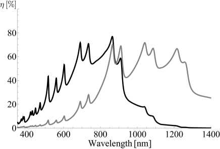
For m nanotubes perpendicular to the fiber, the absorption probabilities as defined by Eq. (43) for different wavelengths of light and different zigzag nanotubes are shown in Fig. 8. We do not consider the absorption of photons with energies greater than 6eV since these are not visible and require the addition of the higher energy orbitals for accurate results. Distinct absorption peaks are clearly visible and the largest absorption occurs for a (11,0) nanotube. The absorption for a nanotube in a linearly polarized coherent plane wave [see Eq. (48)] is also shown in Fig. 8. This beam has a cross-sectional area of and exhibits the same absorption peaks as the fiber, but varies less with the light’s frequency. It can be seen that the (11,0) nanotube has its smallest energy transition dramatically reduced. This extra effect is caused due to larger evanescent fields, for an increasing wavelength relative to the fiber radius. This reduces the field intensity and absorption. The quantum efficiencies are a similar order of magnitude as those observed experimentally for plane waves Freitag et al. (2003); Islam et al. (2004); Berciaud et al. (2008). The different nanotubes show shifted absorption peaks. These can be further adjusted with external fields or choosing other nanotubes Klinovaja et al. (2011); Kim and Chang (2001); Pacheco et al. (2005). The resonant energy values are unchanged with the orientation and this allows us to choose a range to average over as a general measure of absorption. We chose to calculate the mean absorption over the (7,0) nanotube’s lowest absorption energy, particularly we chose a range of 1eV from 1.3eV (953nm) to 2.3eV (539nm). The resulting is approximately independent of in a range of eV to eV deviating only by a few percent.
The corresponding mean absorption against nanotube length, for the lowest energy transition, is shown in Fig. 9 for various angles between the straight nanotube and nanofiber. The results show that the absorption converges to a maximum value as the length is increased, unless the nanotube is parallel to the fiber. The nanotube perpendicular to the fiber has a very strong absorption for short lengths. In this situation we see the absorption increasing strongly with nanotube length which is due to the linear increase in electron number. As the length increases further this effect is counterbalanced by the fact that the field strength decreases exponentially away from the nanofiber. The absorption hardly increases at all after the nanotube exceeds approximately m. However, over these short distances the absorption of the perpendicular nanotube can be improved upon by shifting the nanotube slightly away from a perfectly perpendicular arrangement. The parallel orientation increases slowly but does not peak. This effect will be discussed later in this section and we will find that the probability can be enhanced by spiralling the nanotube to combine both effects. If linear polarized light was used instead of circular polarized light the absorption could be twice as high depending on the nanotube’s position in the nanofiber plane. We also see a difference between angles of , with the higher absorption being dependent on the light’s polarization and propagation.
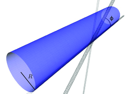
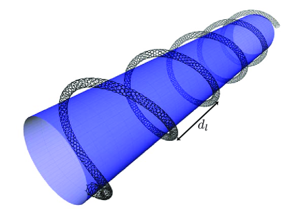
The strong absorption for a perpendicular nanotube is limited by the drop-off in field strength. However, this can be prevented by maintaining a constant distance between the nanotube and nanofiber center, . The nanotube can locally approximate a perpendicular nanotube by spiralling around the nanofiber, as illustrated in Fig. 10. Although this bending does alter the electronic and optical properties these effects are small and can be safely ignored here Koskinen (2010). We define a ‘winding number’, , for the spiral as the number of loops per unit length along the z axis. This winding number is equal to where is the z-distance for one loop. An angle is also formed between the spiralling nanotube and the nanofiber’s direction, which is given by . Since these spiralling nanotubes can interact with the field over an arbitrary length their absorption’s approach given sufficient length and an allowed transition.
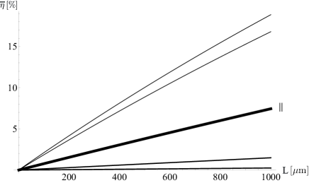
The average absorption probabilities in this case are plotted in Fig. 11 and show a steady increase in the absorption probability with nanotube length. The parallel nanotube is also shown. This demonstrates that the spiralling nanotubes can have higher absorption probabilities than the parallel configuration. In Fig. 12 we have plotted the average absorption probability against for nanotubes of different lengths. An optimal spiralling rate to enhance the absorption can be seen. We found that the optimal value of this winding rate is . This was obtained by maximizing the alignment between the nanotube and .

V Applications
The nanotube-nanofiber setups discussed in the previous sections open up possibilities for a range of applications, particularly highly sensitive photodetectors. These systems would detect light guided within a fiber. In this section we discuss the possibilities. Note that we have only considered the quantum efficiency of the absorption and that detection of the charge excitations is beyond the scope of this paper. However, certain nanotube properties such as ballistic electron transport and low capacitance should be a great advantage for this detection. The bandgap of carbon nanotubes decreases with the nanotube size, so for optical and near infrared wavelengths small diameter nanotubes are required. This rules out the possibility of encasing a nanofiber within a nanotube. Instead, a practical setup is given by arranging horizontal nanotubes in a parallel array and placing the nanofiber orthogonally on top of the array. Based on current nanotube arrays, the density of nanotubes would be nanotubes per Ding et al. (2009); Wang et al. (2010); Sarker et al. (2011); Hong et al. (2010); Shekhar et al. (2011). We will use as a measure of the absorption probability for one nanotube. The photon absorption probability of each nanotube is then, in case of a (7,0) nanotube, given by the top line in Fig. 9 and the overall absorption probability is
| (51) |
Taking (see Fig. 9) this leads to % for , a value greatly exceeding those of currently available APDs Hadfield (2009). For the efficiency exceeds % which can currently only be achieved by highly complex superconducting detectors Hadfield (2009). The advantage of our setup is that it can be operated at room temperature. Each nanotube would require a length of m and has to be connected at the ends by electrodes Wang et al. (2011) which collect the excited electrons via an applied voltage. Although this should be possible in the near future, current technology cannot generate an array of unique nanotubes.
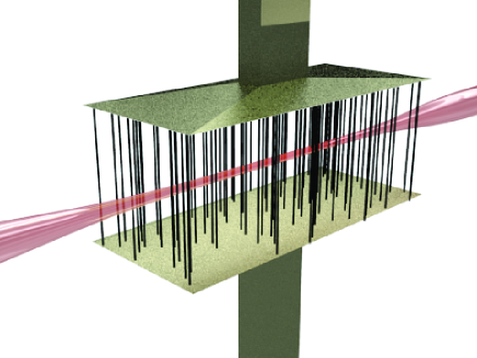
Aligned vertical nanotubes can also be grown on a conducting substrate, that can then serve as one electrode. The nanofiber can then be placed orthogonally to the nanotubes and the remaining ends of the nanotubes connected to an additional electrode (see Fig. 13). The diameter of the nanotubes in this case can be in the range of nm Xu et al. (2006); Hahm et al. (2008). Recently, progress has been made in the generation of such semiconducting nanotube ‘forests’, although a semiconducting nanotube purity of has yet to be achieved reliably Li and Zhang (2011); Qu et al. (2008); Collins et al. (2001). These nanotube systems typically have a density of nanotubes per Zhong et al. (2006); Murakami et al. (2004); Esconjauregui et al. (2010); Ibrahim et al. (2011). The nanotubes are distributed uniformly over a selected region and we assume that they are a uniform mix of semiconducting zigzag nanotubes with a diameter in the range nm. We calculated the overall absorption probability when we have a forest that extends a distance of 500nm from the nanofiber and m along its length, with a density of nanotubes per . The results with nanofibers that have diameters of nm and nm are shown in Fig. 14. These absorb light of a wide range of wavelengths, that can be selected by the nanotubes present and choice of nanofiber diameter. A typical absorption probability of can be seen, for nm diameter fibers, and by extending the system’s length from m to m this is increased to . Nanotubes around a nm fiber are also seen to absorb light at wavelengths that are typically used for optical communication. Due to the nanotube’s bandgap dependence on external fields there is also the possibility of adjusting the absorption frequencies by using an external field.
An additional possible setup is given by arranging the nanofiber and the nanotube parallel to each other. Taking 100 nanotubes of length mm parallel to the fiber and using (see Fig. 11) we obtain an overall absorption probability of which again greatly exceeds that of standard APDs.
As a final setup we consider the coil geometry shown in Fig. 10 which has a high absorption probability of up to 100% for long nanotubes. However, producing such a setup in a laboratory is rather challenging with current technology. This setup also allows for further specification of the absorbed light’s polarization or propagation direction with the choice of winding number. The winding also dramatically reduces the length of the system. For a nanotube with a winding number of , the average absorption between 1.5eV and 2.5eV exceeds when the nanotube’s length is mm. For the nm diameter fiber this only extends m along the fiber.
VI Summary
In this paper we have calculated the probability of absorbing a photon with zigzag carbon nanotubes. The light field is allowed to vary along the nanotube, i.e. no dipole approximation is made, which has enabled us to treat the absorption of light from optical nanofibers. We found that there is a strong dependence on the system’s geometry and have devised setups for high absorption. If we spiral the nanotube around the fiber, we find that an absorption of circularly polarized light, arbitrarily close to 100% can be achieved. For straight nanotubes, that are not parallel to the fiber, we find the absorption probability converges as the nanotube’s length increases. We have found a simple expression for the absorption probability, which is independent of the coherence length. Currently, the coherence lengths of carbon nanotubes is an area of extensive research with results ranging from nm, at room temperature, to a few microns Miyauchi et al. (2009); Roche et al. (2005a); Tans et al. (1997); Roche et al. (2005b); Perebeinos et al. (2005). They seem to be highly dependent on the temperature, impurities, defects and surrounding fields. Once excited, the radiative lifetimes of the excitations have been observed to range from to ns Miyauchi et al. (2009); Wang et al. (2004). The nonradiative decay seems to be much faster, of the order of a few picoseconds Lauret et al. (2003). Introducing excitons into the model and analyzing the dynamics of quantized single photon states within a carbon nanotube is an interesting area of further research. Yet, the results here are an important step towards calculating the absorptions within nanostructures and are of importance to future nanotube optoelectonics.
The research of UD was supported by the Centre for Quantum Technologies, National University of Singapore and the ESF via EuroQUAM (EPSRC Grant No. EP/E041612/1). SB acknowledges support from the EPSRC Doctoral Training Accounts.
Appendix A Calculating the Optical Matrix Element
The matrix element for the interaction between can be found by substituting in the wavefunctions to give
| (52) |
Here we have assumed that the orbitals are symmetric and that is constant across each of the nanotube’s unit cells. The expression for can then be split into separate unit cells and directions
| (53) | ||||
| (54) |
In order to calculate and we must take the curvature of the nanotube into consideration. To do this we use the method from Ref. Jiang et al. (2004) and introduce the parameters
| (55) | ||||
| (56) | ||||
| (57) | ||||
| (58) | ||||
| (59) | ||||
| (60) |
From these we calculate to be
| (61) |
Hence, we obtain
| (62) |
Appendix B Classical Nanofiber Field Modes
For light of wavelength, , and , the field parameters must satisfy the fiber eigenvalue equation Snyder and Love (1983)
| (63) |
with referring to the Bessel function of the first kind and being the modified Bessel function of the second kind. By numerically solving Eq. (63) the value of the propagation constant, , is determined. We also define the parameters , and
| (64) |
Inside the fiber () the guided mode, , have the form
| (65) | ||||
| (66) | ||||
| (67) |
and outside
| (68) | ||||
| (69) | ||||
| (70) |
These are normalized with a factor given by
| (71) |
References
- Charlier et al. (2007) J.-C. Charlier, X. Blase, and S. Roche, Rev. Mod. Phys. 79, 677 (2007).
- Ando (2005) T. Ando, Journal of the Physical Society of Japan 74, 777 (2005).
- Saito et al. (1998) R. Saito, G. Dresselhaus, and M. Dresselhaus, Physical properties of carbon nanotubes (Imperial College Press, 1998).
- Wang et al. (2009) X. Wang, Q. Li, J. Xie, Z. Jin, J. Wang, Y. Li, K. Jiang, and S. Fan, Nano Letters 9, 3137 (2009).
- White and Todorov (1998) C. White and T. Todorov, Nature 393, 240 (1998).
- Klinovaja et al. (2011) J. Klinovaja, M. J. Schmidt, B. Braunecker, and D. Loss, Phys. Rev. Lett. 106, 156809 (2011).
- Kim and Chang (2001) Y.-H. Kim and K. J. Chang, Phys. Rev. B 64, 153404 (2001).
- Pacheco et al. (2005) M. Pacheco, Z. Barticevic, C. G. Rocha, and A. Latgé, Journal of Physics: Condensed Matter 17, 5839 (2005).
- Takesue et al. (2006) I. Takesue, J. Haruyama, N. Kobayashi, S. Chiashi, S. Maruyama, T. Sugai, and H. Shinohara, Phys. Rev. Lett. 96, 057001 (2006).
- Noffsinger and Cohen (2011) J. Noffsinger and M. L. Cohen, Phys. Rev. B 83, 165420 (2011).
- Kasumov et al. (1999) A. Y. Kasumov, R. Deblock, M. Kociak, B. Reulet, H. Bouchiat, I. I. Khodos, Y. B. Gorbatov, V. T. Volkov, C. Journet, and M. Burghard, Science 284, 1508 (1999).
- Morpurgo et al. (1999) A. F. Morpurgo, J. Kong, C. M. Marcus, and H. Dai, Science 286, 263 (1999).
- Uchida and Okada (2009) K. Uchida and S. Okada, Phys. Rev. B 79, 085402 (2009).
- Snow et al. (2005) E. S. Snow, F. K. Perkins, E. J. Houser, S. C. Badescu, and T. L. Reinecke, Science 307, 1942 (2005).
- Tang et al. (2006) X. Tang, S. Bansaruntip, N. Nakayama, E. Yenilmez, Y.-l. Chang, and Q. Wang, Nano Letters 6, 1632 (2006).
- Freitag et al. (2003) M. Freitag, Y. Martin, J. A. Misewich, R. Martel, and P. Avouris, Nano Letters 3, 1067 (2003).
- Spataru et al. (2004) C. D. Spataru, S. Ismail-Beigi, L. X. Benedict, and S. G. Louie, Phys. Rev. Lett. 92, 077402 (2004).
- Jiang et al. (2004) J. Jiang, R. Saito, A. Grüneis, G. Dresselhaus, and M. Dresselhaus, Carbon 42, 3169 (2004).
- Motavas et al. (2010) S. Motavas, A. Ivanov, and A. Nojeh, Phys. Rev. B 82, 085442 (2010).
- Zarifi and Pedersen (2009) A. Zarifi and T. G. Pedersen, Phys. Rev. B 80, 195422 (2009).
- Goupalov et al. (2010) S. V. Goupalov, A. Zarifi, and T. G. Pedersen, Phys. Rev. B 81, 153402 (2010).
- Goupalov (2005) S. V. Goupalov, Phys. Rev. B 72, 195403 (2005).
- Berciaud et al. (2010) S. Berciaud, C. Voisin, H. Yan, B. Chandra, R. Caldwell, Y. Shan, L. E. Brus, J. Hone, and T. F. Heinz, Phys. Rev. B 81, 041414 (2010).
- Takagi and Okada (2009) Y. Takagi and S. Okada, Phys. Rev. B 79, 233406 (2009).
- Zarifi and Pedersen (2006) A. Zarifi and T. G. Pedersen, Phys. Rev. B 74, 155434 (2006).
- Malić et al. (2006) E. Malić, M. Hirtschulz, F. Milde, A. Knorr, and S. Reich, Phys. Rev. B 74, 195431 (2006).
- Saito et al. (2004) R. Saito, A. Gruneis, G. Samsonidze, G. Dresselhaus, M. Dresselhaus, A. Jorio, L. Cancado, M. Pimenta, and A. Souza, Applied Physics A 78, 1099 (2004).
- Miyauchi et al. (2009) Y. Miyauchi, H. Hirori, K. Matsuda, and Y. Kanemitsu, Phys. Rev. B 80, 081410 (2009).
- Roche et al. (2005a) S. Roche, J. Jiang, F. m. c. Triozon, and R. Saito, Phys. Rev. Lett. 95, 076803 (2005a).
- Tans et al. (1997) S. Tans, M. Devoret, H. Dai, A. Thess, R. Smalley, L. Geerligs, and C. Dekker, Nature 386, 474 (1997).
- Roche et al. (2005b) S. Roche, J. Jiang, F. m. c. Triozon, and R. Saito, Phys. Rev. B 72, 113410 (2005b).
- Perebeinos et al. (2005) V. Perebeinos, J. Tersoff, and P. Avouris, Phys. Rev. Lett. 94, 086802 (2005).
- Bures and Ghosh (1999) J. Bures and R. Ghosh, J. Opt. Soc. Am. A 16, 1992 (1999).
- Le Kien et al. (2005) F. Le Kien, S. D. Gupta, K. P. Nayak, and K. Hakuta, Phys. Rev. A 72, 063815 (2005).
- Sagué et al. (2007) G. Sagué, E. Vetsch, W. Alt, D. Meschede, and A. Rauschenbeutel, Phys. Rev. Lett. 99, 163602 (2007).
- Vetsch et al. (2010) E. Vetsch, D. Reitz, G. Sagué, R. Schmidt, S. T. Dawkins, and A. Rauschenbeutel, Phys. Rev. Lett. 104, 203603 (2010).
- Liao et al. (2008) A. Liao, Y. Zhao, and E. Pop, Phys. Rev. Lett. 101, 256804 (2008).
- Dresselhaus et al. (2007) M. S. Dresselhaus, G. Dresselhaus, R. Saito, and A. Jorio, Annual Review of Physical Chemistry 58, 719 (2007).
- Bunder and Hill (2009) J. E. Bunder and J. M. Hill, Phys. Rev. B 80, 153406 (2009).
- Mohite et al. (2008) A. D. Mohite, P. Gopinath, H. M. Shah, and B. W. Alphenaar, Nano Letters 8, 142 (2008).
- Ichida et al. (1999) M. Ichida, S. Mizuno, Y. Tani, Y. Saito, and A. Nakamura, Journal of the Physical Society of Japan 68, 3131 (1999).
- Abergel et al. (2010) D. Abergel, V. Apalkov, J. Berashevich, K. Ziegler, and T. Chakraborty, Advances in Physics 59, 261 (2010).
- Grüneis et al. (2003) A. Grüneis, R. Saito, G. G. Samsonidze, T. Kimura, M. A. Pimenta, A. Jorio, A. G. S. Filho, G. Dresselhaus, and M. S. Dresselhaus, Phys. Rev. B 67, 165402 (2003).
- Saito et al. (2000) R. Saito, G. Dresselhaus, and M. S. Dresselhaus, Phys. Rev. B 61, 2981 (2000).
- Nikolaev et al. (2009) A. V. Nikolaev, A. V. Bibikov, A. V. Avdeenkov, I. V. Bodrenko, and E. V. Tkalya, Phys. Rev. B 79, 045418 (2009).
- Blow et al. (1990) K. J. Blow, R. Loudon, S. J. D. Phoenix, and T. J. Shepherd, Phys. Rev. A 42, 4102 (1990).
- Tasaki et al. (1998) S. Tasaki, K. Maekawa, and T. Yamabe, Phys. Rev. B 57, 9301 (1998).
- Ajiki and Ando (1994) H. Ajiki and T. Ando, Physica B: Condensed Matter 201, 349 (1994).
- Islam et al. (2004) M. F. Islam, D. E. Milkie, C. L. Kane, A. G. Yodh, and J. M. Kikkawa, Phys. Rev. Lett. 93, 037404 (2004).
- Lauret et al. (2003) J.-S. Lauret, C. Voisin, G. Cassabois, C. Delalande, P. Roussignol, O. Jost, and L. Capes, Phys. Rev. Lett. 90, 057404 (2003).
- Lin (2000) M. F. Lin, Phys. Rev. B 62, 13153 (2000).
- Tong et al. (2003) L. Tong, R. Gattass, J. Ashcom, S. He, J. Lou, M. Shen, I. Maxwell, and E. Mazur, Nature 426, 816 (2003).
- Tong and Mazur (2008) L. Tong and E. Mazur, Journal of Non-Crystalline Solids 354, 1240 (2008), proceedings of the 2005 International Conference on Glass - In conjunction with the Annual Meeting of the International Commission on Glass.
- Brambilla et al. (2004) G. Brambilla, V. Finazzi, and D. Richardson, Opt. Express 12, 2258 (2004).
- Tong (2010) L. Tong, Frontiers of Optoelectronics in China 3, 54 (2010).
- Tong et al. (2004) L. Tong, J. Lou, and E. Mazur, Optics Express 12, 1025 (2004).
- Snyder and Love (1983) A. Snyder and J. Love, Optical waveguide theory, Science paperbacks (Chapman and Hall, 1983).
- Berciaud et al. (2008) S. Berciaud, L. Cognet, and B. Lounis, Phys. Rev. Lett. 101, 077402 (2008).
- Koskinen (2010) P. Koskinen, Phys. Rev. B 82, 193409 (2010).
- Ding et al. (2009) L. Ding, A. Tselev, J. Wang, D. Yuan, H. Chu, T. P. McNicholas, Y. Li, and J. Liu, Nano Letters 9, 800 (2009).
- Wang et al. (2010) C. Wang, K. Ryu, L. De Arco, A. Badmaev, J. Zhang, X. Lin, Y. Che, and C. Zhou, Nano Research 3, 831 (2010).
- Sarker et al. (2011) B. K. Sarker, S. Shekhar, and S. I. Khondaker, ACS Nano 5, 6297 (2011).
- Hong et al. (2010) S. W. Hong, T. Banks, and J. A. Rogers, Advanced Materials 22, 1826 (2010).
- Shekhar et al. (2011) S. Shekhar, P. Stokes, and S. I. Khondaker, ACS Nano 5, 1739 (2011).
- Hadfield (2009) R. H. Hadfield, Nature Photonics 3, 696 (2009).
- Wang et al. (2011) H. Wang, J. Luo, F. Schäffel, M. H. Rümmeli, G. A. D. Briggs, and J. H. Warner, Nanotechnology 22, 245305 (2011).
- Xu et al. (2006) Y.-Q. Xu, E. Flor, M. J. Kim, B. Hamadani, H. Schmidt, R. E. Smalley, and R. H. Hauge, Journal of the American Chemical Society 128, 6560 (2006).
- Hahm et al. (2008) M. G. Hahm, Y.-K. Kwon, E. Lee, C. W. Ahn, and Y. J. Jung, The Journal of Physical Chemistry C 112, 17143 (2008).
- Li and Zhang (2011) P. Li and J. Zhang, J. Mater. Chem. 21, 11815 (2011).
- Qu et al. (2008) L. Qu, F. Du, and L. Dai, Nano Letters 8, 2682 (2008).
- Collins et al. (2001) P. G. Collins, M. S. Arnold, and P. Avouris, Science 292, 706 (2001).
- Zhong et al. (2006) G. F. Zhong, T. Iwasaki, and H. Kawarada, Carbon 44, 2009 (2006).
- Murakami et al. (2004) Y. Murakami, S. Chiashi, Y. Miyauchi, M. Hu, M. Ogura, T. Okubo, and S. Maruyama, Chemical Physics Letters 385, 298 (2004).
- Esconjauregui et al. (2010) S. Esconjauregui, M. Fouquet, B. C. Bayer, C. Ducati, R. Smajda, S. Hofmann, and J. Robertson, ACS Nano 4, 7431 (2010).
- Ibrahim et al. (2011) I. Ibrahim, A. Bachmatiuk, F. Börrnert, J. Blüher, U. Wolff, J. H. Warner, B. Büchner, G. Cuniberti, and M. H. Rümmeli, Carbon 49, 5029 (2011).
- Wang et al. (2004) F. Wang, G. Dukovic, L. E. Brus, and T. F. Heinz, Phys. Rev. Lett. 92, 177401 (2004).