Extraordinary transmission caused by symmetry breaking
Abstract
The terahertz transmission properties of symmetrical and asymmetrical annular apertures arrays (AAAs) are investigated both experimentally and numerically. It is found that only odd order resonant modes are observed for the symmetrical structures but both odd and even order resonances can be shown for the asymmetrical structures. Breaking the symmetry of AAAs by gradually displacing the H-shaped AAAs to U-shaped AAAs allows an intensity modulation depth of of the second order resonance. Simulation results verify the experimental conclusions well. This result provides a tremendous opportunity for terahertz wavelength tunable filtering, sensing, and near-field imaging.
pacs:
78.20.Ci, 42.25.BsSince the extraordinary transmission (EOT) phenomenon of sub-wavelength metallic apertures arrays has been reported by Ebbesen and his co-workers Ebbesen98 ; Barnes99 , it has been paid extensive attentions to understand the underlying physical mechanisms Ghaemi98 ; Maier07 . Although it is still debated on the real mechanism of the EOT, surface plasmon polaritons (SPPs) originating from the coupling of light with the surface charges oscillation on the metal-dielectric interface Ghaemi98 and the localized surface plasmon resonance (LSPR) excited on the hole ridge are recognized as the main possible contributions to the EOT Maier07 . Moreover, it has been shown that the transmission spectral response of sub-wavelength metallic apertures arrays are affected by the cell size Molen04 , cell shape Lee06 ; Lee09 , lattice periodicity Lee10 , metal film thickness Wang09 , the refractive index of the adjacent medium Azad05 , as well as the polarization of incident light Masson06 . Annular aperture arrays (AAAs) have also been demonstrated to have EOT Poujet07 ; Lu10 . The influence of geometric and structure parameters of the AAAs on the EOT properties has been extensively investigated. However, the influences of the symmetry of the AAAs on the EOT have not been reported. In this Letter, the transmission properties of the symmetric and asymmetric AAAs are investigated both experimentally and theoretically. The interactions of the terahertz (THz) electromagnetic radiation with the AAAs have been measured with the traditional THz time domain spectroscopy (TDS). The field distributions of the resonant wavelengths are simulated with the finite difference time domain (FDTD) method. The physical original of the resonant enhanced transmission has been analyzed. It is found that the symmetry breaking can enhance the even order mode EOT.

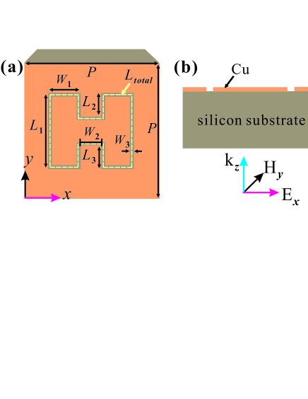
The proposed AAAs structure is schematically shown in Fig. 1. It is a H-shaped annular slit. The outer arm length of the H-shaped slit is , the upper and lower inner arm lengths are and , the outer and inter arm widthes are and , respectively. The slit width is and the period () of the sample is . This sample is symmetrical along both and directions. The total average circumference of the AAAs, which is the average length of out and inner edge of the slit, is denoted as . The samples are fabricated onto a thin copper film () with the conventional photolithography and metallization processes. The substrate is a thick doubly polished p-type silicon wafer.
The transmission spectra of the samples are measured by using a typical THz TDS. The THz wave pulses are generated from a dipole-type photoconductive antenna illuminated by a laser with center wavelength. The valid range of the system is . The detection is achieved by a ZnTe crystal. For the reference, a bare silicon wafer identical to the one on which the AAAs are fabricated is used. The transmitted THz pulses are measured at normal incidence such that the electric and magnetic field of the incident radiation are in AAAs’ plane. All measurements are done at room temperature and in a dry atmosphere to mitigate water absorption. The normalized transmittance is obtained by , where and are Fourier transformed transmitted electric field of the sample and reference pulses, respectively.

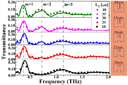
The transmission spectra of five samples with different are shown in Fig. 2 with symbols. The parameters of the structures are selected as follows: The widthes and are and , respectively. The length is . The length increases from to with step of and thus reduces from to . The average circumference of the slit is kept as a constant as . For , the sample is H-shaped AAAs and symmetrical along both and directions. For and , the sample becomes to U-shaped AAAs and it is only symmetry along the direction. It can be seen that two resonance peaks at and appear in all transmission spectra. With increasing, the symmetry of the structure along the direction has been broken, the locations of these two peaks nearly unchanged but a new resonance peak appears at . The transmission for is enhanced from for symmetrical structure to for asymmetrical one, the intensity modulation depth is .
For the AAAs structure, the localized surface plasmonics will be excited under the light illumination. The surface charges are assembled at the edge of the metal. Based on the basic idea of Ref. Neubrech06 , the resonance appears when the following condition is satisfied:
| (1) |
where is the resonant frequency, is an integer which is the order of the resonant mode, is the speed of light in vacuum, is the average circumference of the AAAs, and is the effective refraction index for the localized surface plasmonic wave. In our case, is approximatively equal to , is the refraction index of the substrate. Under this condition, the standing wave of the localized surface plasmon can be generated along the wedges of the metallic film. Furthermore, the distribution of localized surface plasmon should also satisfy the symmetry requirement of the samples. All samples considered here are symmetrical along the direction and the illumination light is polarized along the direction, thus the distribution of the assembled surface charges should be antisymmetrical along the direction. If the sample is also symmetrical along the direction, the distribution of the assembled surface charges should also be even symmetrical along the direction. When the distribution of the assembled surface charges satisfy both the standing wave condition and symmetry condition, the corresponding transmission can be greatly enhanced. For all samples considered here, the odd mode (for example, or ) can easily satisfies these requirements no matter the sample is symmetrical along the direction or not. However, if the resonant mode is even, the symmetry of the sample along the direction will affect the distribution of the surface charges and hence the transmission amplitude. It requires the distribution of the surface charges is also symmetrical along the direction. Thus, the standing wave condition for second mode can not be stratified any more, therefore, the transmission for the second resonant mode will be greatly reduced, as shown in Fig. 2 with . But when the symmetry along the direction is broken, the requirement of the symmetry of surface charge distribution along this direction does not exist, the standing wave of the localized surface plasmon can be generated and the resonant peak appears, as shown in Fig. 2 with .
In order to get an insight into the nature of the resonant transmission for the proposed structures, the numerical simulations are carried out by using the FDTD approach Simulations . The metal copper is described by the perfect electric conductor to fit its realistic characteristic in the terahertz range. The refraction indices of the air and substrate silicon are set as 1.0 and 3.31 in the simulations, respectively. The calculated transmission spectra are also shown in Fig. 2 with solid lines. It can be found that the simulation results correspond to the experiment measurements well. From the simulation results, it can also be found that the sample with has two resonant peaks at and , which correspond to and , respectively. But the sample with has three resonant peaks. A new peak corresponding to appears at . With increasing, the transmission for the second resonant mode enhanced.

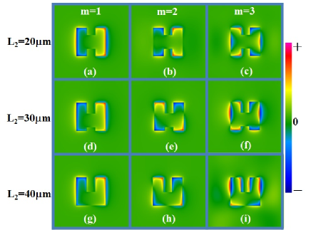
Figure 3 presents the extremum electric field distributions at the aforementioned three resonant frequencies for samples with equals , , and , respectively, which exhibits the distributions of the surface charges. When the structure is symmetrical along both and directions, it can be found from Fig. 3(a)-(c) that the extremum electric field distributions are antisymmetrical along the direction but symmetrical along the direction. These are natural results for satisfying the symmetrical requirement of the samples. For the odd modes and (correspond to Fig. 3(a) and (c), respectively), the standing waves are generated along the edges of the metallic film. One wave crest along the out side of slit in Fig. 3(a) and three crests in Fig. 3(c) can be found. However, in order to satisfy the symmetry condition along the direction, the surface charge wave can not generate a standing wave with mode , as shown in Fig. 3(b). Only a temporarily electric field distribution is shown here and no standing wave distribution can be found. For the structure with , the electric field distributions are also antisymmetrical along the direction. Since the structure is not symmetrical along the direction any more, the surface charges distributions are not required to be symmetrical along the direction. There are 1, 2, and 3 standing waves generated for mode (Fig. 3(g)), (Fig. 3(h)) and (Fig. 3(i)), respectively. The even mode standing wave is formed and thus the corresponding transmission has been enhanced. It can be concluded that the resonant peak for the structure with is caused by the symmetry breaking along the direction.
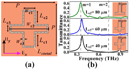
For further validation, the transmission spectra for another series of structures are calculated and shown in Fig. 4. The AAAs is cross shaped and the average circumference is still . The girder is shifted from the middle to the bottom of the cross to break the symmetry along the direction. It can be seen from the transmission spectra that the odd mode appears around for all structures. However, the transmission intensity for second mode increases from for symmetrical structure to for the asymmetrical structure. These results also demonstrate that the symmetry breaking can enhance the odd mode resonance.

In summary, the transmission characteristics of the symmetrical and asymmetrical AAAs with narrow gap are investigated experimentally and numerically. The measured and simulated transmission spectra reveal that the resonant transmission are affected by the geometric structure. Both even and odd order modes can emerge for the asymmetrical AAAs but only odd order modes appears for the symmetrical AAAs. The appearance of the even mode is caused by the symmetry breaking. This research indicates a new freedom in tuning the electromagnetic response, which offers a path to design more robust plasmonic devices.
This work was supported by the 973 Program of China (No. 2011CB301801) and National Natural Science Foundation of China (No. 10904099 and 11174211).
References
- (1) T. W. Ebbesen, H. J. Lezec, H. F. Ghaemi, T. Thio, and P. A. Wolff, Nature (London)424, 824 (1998).
- (2) W. L. Barnes, A. Dereux, and T. W. Ebbesen, Nature (London)391, 667 (2003).
- (3) H. F. Ghaemi, T. Thio, D. E. Grupp, T. W. Ebbesen, and H. J. Lezec,Phys. Rev. B58, 6779 (1998).
- (4) S. A. Maier, Plasmonics: Fundamentals and Applications (Springer, New York, 2007).
- (5) K. L. V. Molen, F. B. Segerink, N. F. V. Hulst, and L. Kuipersb, Appl. Phys. Lett. 85, 4316 (2004).
- (6) J. W. Lee, M. A. Seo, D. J. Park, D. S. Kim, S. C. Jeoung , C. Lienau, Q. H. Park and P. C. M. Planken, Opt. Express 14, 1253 (2006).
- (7) J. W. Lee, M. A. Seo, D. S. Kim, J. H. Kang, and Q-Han Park, Appl. Phys. Lett. 94, 081102 (2009).
- (8) J. W. Lee, T. H. Park, P. Nordlander, and D. M. Mittleman, Appl. Phys. Lett. 97, 261112 (2010).
- (9) W. Wang, Y. L. Lu, R. J. Knize, K. Reinhardt, and S. C. Chen, Opt. Express 17, 7361 (2009).
- (10) A. K. Azad, Y. Zhao, and W. L. Zhang, Appl. Phys. Lett. 86, 141102 (2005).
- (11) J. B. Masson and G. Gallot, Phys. Rev. B73, 121401(R) (2006).
- (12) Y. Poujet, J. Salvi, and F. I. Baida, Opt. Lett. 32, 2942 (2007).
- (13) X. C. Lu, J. G. Han, and W. L. Zhang, Opt. Lett. 35, 070904 (2010).
- (14) F. Neubrech, T. Kolb, R. Lovrincic, G. Fahsold, A. Puccia, J. Aizpurua, T. W. Cornelius, M. E. T. Molares, R. Neumann, and S. Karim, Appl. Phys. Lett. 89, 253104 (2006).
- (15) Simulations were performed using the software package CONCERTO 7.5R, developed by Vector Fields Limited, England, 2011.