Thickness dependence of structural and transport properties of Co-doped BaFe2As2 on Fe buffered MgO substrates
Abstract
We have investigated the influence of the superconducting layer thickness, , on the structural and transport properties of Co-doped BaFe2As2 films deposited on Fe-buffered MgO substrates by pulsed laser deposition. The superconducting transition temperature and the texture quality of Co-doped BaFe2As2 films improve with increasing due to a gradual relief of the tensile strain. For an additional 110 textured component of Co-doped BaFe2As2 was observed, which leads to an upward shift in the angular dependent critical current density at . These results indicate that the grain boundaries created by the 110 textured component may contribute to the -axis pinning.
pacs:
74.70.Xa, 81.15.Fg, 74.78.-w, 74.25.Sv, 74.25.F-1 Introduction
Crystalline quality, structural parameters and surface morphology of thin films are generally influenced by their thickness due to several factors such as strain, defect formation and change in growth mode. Such changes affect the physical properties of thin films. Hence, whenever new functional thin films are prepared, it always becomes immediately interesting to explore the effect of layer thickness on the structural and physical properties.
Among the family of newly discovered Fe-based superconducting compounds, increasing the layer thickness of FeSe and FeSe0.5Te0.5 thin films improves the superconducting transition temperature, , presumably due to lattice distortion by strain [1, 2].
For Co-doped BaFe2As2 (Ba-122) films, only thickness studies regarding the buffer layers have been reported to date. Tarantini and Lee have found that single crystalline (La,Sr)(Al,Ta)O3 substrates with 100 unit cells of epitaxial SrTiO3 resulted in the highest and the largest critical current density, [3, 4]. Even higher and sharper out-of-plane and in-plane textures of the Fe/Ba-122 bilayers can be realized for 20 nm thick epitaxial Fe buffer layers [5]. However, no investigation of the effect of layer thickness of Co-doped Ba-122 on the structural and transport properties have been published to date. In this article, we report on the influence of layer thickness on the structural and transport properties of the Fe/Ba-122 bilayer system with a fixed Fe layer thickness.
2 Experiment
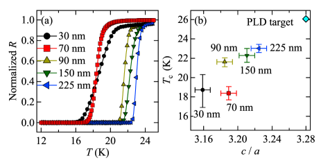
Epitaxial, smooth Fe buffer layers (20 nm) were prepared by a two-step process, which involves a room temperature deposition of Fe on MgO (001) single crystalline substrates by pulsed laser deposition, PLD, followed by a high-temperature annealing at 750 ∘C, both in a UHV chamber (base pressure of 10-10 mbar). Prior to the Fe deposition, the substrate was heated to 1000 ∘C, held at this temperature for 30 min, subsequently cooled to room temperature for cleaning. A KrF excimer laser (248 nm) has been employed at a frequency of 5 Hz for the deposition with an energy density of 3–5 Jcm-2 on the target. After the Fe buffer preparation, Co-doped Ba-122 layers were deposited at 750 ∘C with a laser repetition rate of 10 Hz. Each deposition step was monitored by reflection high-energy electron diffraction, RHEED. The layer thickness, , was varied in the range of 30 nm to 225 nm by controlling the number of laser pulses. Each layer thickness was confirmed by cross-sectional focused ion beam, FIB, cuts on multiple sample areas. The nominal composition of the PLD target was Ba:Fe:Co:As = 1:1.84:0.16:2. The detailed target preparation can be found in reference [6]. The phase purity of the target was determined by x-ray diffraction using a standard Bragg-Brentano geometry with Co-K radiation. All the observed peaks were identified as Co-doped Ba-122. The lattice parameters refined via Rietveld analyses were nm and nm, respectively.
Surface morphology of the films was observed by atomic force microscopy, AFM. Out-of-plane texture and phase purity were investigated by x-ray diffraction in Bragg-Brentano geometry with Co-K radiation. In-plane orientation of both Fe and Co-doped Ba-122 were investigated by using the 110 and 103 poles respectively in a texture goniometer operating with Cu-K radiation. In order to evaluate the in-plane and out-of-plane lattice parameters of Co-doped Ba-122 precisely, high resolution reciprocal space maps, RSM, around the 109, 1011 and 1110 reflections were performed with Cu-K radiation. Here, the 204 reflection of MgO was used as a reference to eliminate any errors by a misalignment of the substrate.
After the structural characterization, Au layers were deposited on the films by PLD at room temperature followed by ion beam etching to form bridges of 0.5 mm width and 1 mm length for transport measurements. Superconducting properties were measured in a Physical Property Measurement System (PPMS, Quantum Design) by a standard four-probe method with a criterion of 1 for evaluating . In the angular-dependent measurements, , the magnetic field, , was applied in the maximum Lorentz force configuration ( perpendicular to ) at an angle measured from the -axis. is defined as 50% of the normal state resistance at 30 K.
3 Results and discussion
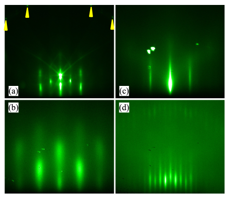
The diffraction pattern in the RHEED images of MgO substrate shows a series of spots lying on the Laue circles, indicative of a perfectly flat surface (figure 1(a)). For the Fe buffer preparation, the RHEED images of Fe in figure 1(b) confirm the epitaxial growth even at room temperature for =150 nm. The diffraction spots turn into streaks with increasing temperature (figure 1(c)), indicative of smoothing of the surface [7]. For Co-doped Ba-122, the diffraction patterns with long streaks centered at positions on the Laue circles is typical for a multilevel surface (figure 1(d)); i.e. for a high number of smooth terraces separated by steps [7]. Additionally, the spacing of the observed streaks indicates a surface reconstruction, which is consistent with the observation on single crystals reported in reference [8].
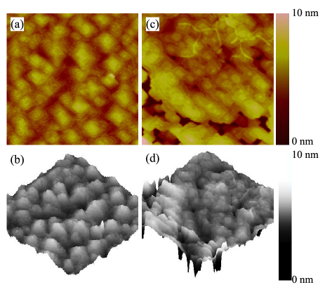
The AFM image of this film in figures 2 (a) and (b) further confirmed that the surface was flat with a root mean-square roughness, , of 0.83 nm. The AFM image also shows that Co-doped Ba-122 grows in the terraced-island mode with an average step height of 0.65 nm, which is almost identical to half the lattice parameter . All the films in this study have the same surface morphology, and their surface roughness are summarized in Table 1. However, the grains of the 30 nm thick film are smaller and not well connected compared with the other films (figures. 2(c) and (d)).
The - scans for the Fe/Ba-122 bilayers with different layer thickness do not show any secondary phases (figure 3). The pronounced 00 reflections of Co-doped Ba-122 together with the 002 reflection of MgO and Fe are observed for all films, indicating a -axis orientation. For thickness , a 110 component is observed whose intensity becomes gradually stronger with increasing . In addition, the ratio of the diffraction intensity for the 110 and 004 is increased with (Table 1). This 110 component is also visible in the 103 pole figure measurement, and its epitaxial relation to the substrate is (110)[001]Ba-122(001)[110]MgO and (110)[001]Ba-122(001)[10]MgO. It should be noted, however, that the amount of the 110 component is small since the ratio of the diffraction intensity for the 110 and 004 is less than 0.01 for all films. Here, the corresponding value for a randomly oriented grain is 3.28 (ICDD card number 01-077-6875). Indeed, this small amount of 110 component does not compromise the crystalline quality as shown in Table 1. The full width at half maximum (FWHM), , of the 004 rocking curve and the average of the 103 reflection of Co-doped Ba-122 are getting smaller with increasing .
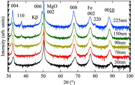
Another prominent feature is a shift of the 00 reflections to lower angles with increasing , indicating an increase in the lattice parameter . Calculated lattice parameters of the films using the Nelson-Riley function are increasing from 1.274 nm () to 1.289 nm () [9], as shown in Table 1. 1. In this calculation, the 002 reflection is omitted in order to avoid excessive extrapolation. The correlation between the layer thickness and both the in-plane and the out-of-plane lattice parameters evaluated by RSM are exhibited in figures 4 (a) and (b). The lattice parameter is observed to decrease with , while the out-of-plane lattice parameter behaves the opposite way. The evaluated lattice parameter by both methods (i.e. RSM and the - scans) are almost identical for all the films within the experimental uncertainty, albeit high angle data of are not measured in the - scans. Since the FeAs tetrahedron in the Ba-122 bonds coherently to bcc Fe [10], the lattice parameter of a thin Co-doped Ba-122 layer is close to that of Fe multiplied by (0.4053 nm), which is slightly larger than of bulk Co-doped Ba-122 (i.e. PLD target), suggesting tensile strain in the film. The lattice parameter of Fe is almost constant at around 0.287 nm confirmed by RSM. Here the respective lattice misfit of Fe/MgO and Co-doped Ba-122/Fe are -3.9% and -2.4%.
| (nm) | (nm) | (nm) | / | ||
|---|---|---|---|---|---|
| 30 | 1.14 | 0.82 | 0.99 | 1.274 | n. d. |
| 70 | 0.85 | 0.96 | 1.26 | 1.285 | n. d. |
| 90 | 1.47 | 0.65 | 0.88 | 1.284 | |
| 150 | 0.83 | 0.67 | 0.92 | 1.288 | 0.003 |
| 225 | 2.11 | 0.60 | 0.81 | 1.289 | 0.007 |
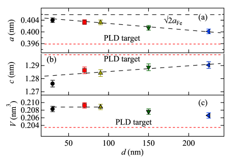
The unit cell volume, , of Co-doped Ba-122 films is almost constant with in the range of , while the thicker films deviate from this trend presumably due to a relatively large contents of grain boundaries, GBs (figure 4(c)). Nevertheless, the volume for all the films is larger than that of the bulk Co-doped Ba-122, which might be due to As deficiency. The correlation between the lattice parameters and As deficiency for Co-doped Ba-122 is not clear. However, both the in-plane and the out-of-plane lattice parameters of As-deficient LaFeAsOF are enlarged compared with that of the stoichiometric sample [11], resulting in a larger lattice volume of the As-deficient sample.
Shown in figure 5 (a) are the normalized resistive traces of the Co-doped Ba-122 with different . The film with shows the lowest of around 18 K. The 30 nm thick film shows a broad transition width, which is a direct consequence of the small grain size together with poor connectivity. Another prominent feature is a clear jump of between 70 nm and 90 nm thickness. From the - scans in figure 3, the 110 component is absent in the 70 nm thick film whereas the 90 nm thick film contained a small amount of the 110 grains. For , the s are gradually improved up to 23 K together with sharpening of the transition width by increasing . It is clear from figure 5 (b) that of the films improves with , which is consistent with our previous results for films on different substrates [6].
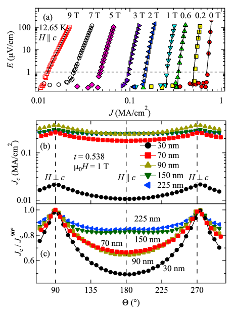
The curves for the Co-doped Ba-122 film with measured in various magnetic fields at 12.65 K show a power-law relation, indicative of current limitation by depinning of flux lines rather than GB effects (figure 6 (a)). As stated earlier, thicker films contained a small amount of the 110 component. However, the film does not show any sign of weak-link behavior.
The measured at a reduced temperature of (, where the is onset temperature of zero resistance) are exhibited in figure 6 (b). All the films except the 30 nm thick film can carry a high of over in the whole angular range. The 30 nm thick film shows one order of magnitude lower than that of the other films, which is due to the small grain size together with poor connectivity. Indeed, curves of this film show a non-ohmic linear differential, NOLD, signature, indicative of limitation by GBs [12].
Another prominent feature is a shift upward of at ( ) as the thickness of Co-doped Ba-122 films increases. In particular a small -axis angular peak is observed for (fig. 6 (c)). These films show very similar forms of with a low anisotropy, . For example, of the film with is only around 1.2, whereas the corresponding values of the 90 nm and 30 nm thick films are 1.5 and 2, respectively. These results suggest that the GBs may contribute to the pinning along the -axis [13], which opens the opportunity to tune by controlling the amount of the 110 textured component.
The implementation of very thin Fe buffer layers also yields the 110 textured component [5]. However, the crystalline quality and the superconducting properties of Co-doped Ba-122 are compromised due to the presence of too many GBs. Hence, there may exist a threshold of the amount of GBs at which deterioration of the structural and superconducting properties sets in.
4 Conclusion
The effect of the superconducting layer thickness on the structural and superconducting properties of Co-doped Ba-122 films has been investigated. The texture quality and the superconducting transition temperature are improved by increasing the layer thickness due to stress relief. Increasing the layer thickness yields an additional 110 textured component, creating GBs. However, these GBs may constitute -axis pinning centers within a certain amount, which leads to an increase in at without compromising the structural and superconducting properties.
References
References
- [1] Wang M J, Luo J Y, Huang T W, Chang H H, Chen T K, Hsu F C, Wu C T, Wu P M, Chang A M and Wu M K 2009 Phys. Rev. Lett.103 117002
- [2] Bellingeri E, Pallecchi I, Buzio R, Gerbi A, Marré D, Cimberle M R, Tropeano M, Putti M, Palenzona A and Ferdeghini C 2010 Appl. Phys. Lett. 96 102512
- [3] Tarantini C, Lee S, Zhang Y, Jiang J, Bark C W, Weiss J D, Polyanskii A, Nelson C T, Jang H W, Folkman C M, Baek S H, Pan X Q, Gurevich A, Hellstrom E E, Eom C B and Larbalestier D C 2010 Appl. Phys. Lett. 96 142510
- [4] Lee S, Jiang J, Weiss J D, Bark C W, Tarantini C, Biegalski M D, Polyanskii A, Zhang Y, Nelson C T, Pan X Q, Hellstrom E E, Larbalestier D C and Eom C B 2011 IEEE Trans. Appl. Supercond. 21 2882
- [5] Iida K, Haindl S, Thersleff T, Hänisch J, Kurth F, Kidszun M, Hühne R, Mönch I, Schultz L, Holzapfel B and Heller R 2010 Appl. Phys. Lett. 97 172507
- [6] Iida K, Hänisch J, Hühne R, Kurth F, Kidszun M, Haindl S, Werner J, Schultz L and Holzapfel B 2009 Appl. Phys. Lett. 95 192501
- [7] Lagally M G, Savage D E and Tringides M C 1988 Reflection High-Energy Electron Diffraction and Reflection Electron Imaging of Surfaces (NATO ASI Ser. B vol 188) ed Larsen P K and Dobson P J (Plenum, New York)
- [8] van Heumen E, Vuorinen J, Koepernik K, Massee F, Huang Y, Shi M, Klei J, Goedkoop J, Lindroos M, van den Brink J and Golden M S 2011 Phys. Rev. Lett.106 027002
- [9] Nelson J B and Riley D P 1945 Proc. Phys. Soc. 57 160
- [10] Thersleff T, Iida K, Haindl S, Kidszun M, Pohl D, Hartmann A, Kurth F, Hänisch J, Hühne R, Rellinghaus B, Schultz L and Holzapfel B 2010 Appl. Phys. Lett. 97 022506
- [11] Fuchs G, Drechsler S L, Kozlova N, Behr G, Köhler A, Werner J, Nenkov K, Klingeler R, Hamann-Borrero J, Hess C, Kondrat A, Grobosch M, Narduzzo A, Knupfer M, Freudenberger J, Büchner B and L. Schultz 2008 Phys. Rev. Lett.101 237003
- [12] Verebelyi D T, Christen D K, Feenstra R, Cantoni C, Goyal A, Lee D F, Paranthaman M, Arendt P N, DePaula R F, Groves J R and Prouteau C 2000 Appl. Phys. Lett. 76 1755
- [13] Katase T, Hiramatsu H, Matias V, Sheehan C, Ishimaru Y, Kamiya T, Tanabe K and Hosono H 2011 Appl. Phys. Lett. 98 242510