Characterisation of a Thin Fully-Depleted SOI Pixel Sensor with Soft X-ray Radiation
Abstract
This paper presents the results of the characterisation of a back-illuminated pixel sensor manufactured in Silicon-On-Insulator technology on a high-resistivity substrate with soft X-rays. The sensor is thinned and a thin Phosphor layer contact is implanted on the back-plane. The response to X-rays from 2.12 up to 8.6 keV is evaluated with fluorescence radiation at the LBNL Advanced Light Source.
keywords:
Monolithic pixel sensor; SOI; CMOS technology; Particle detection.1 Introduction
The availability of the ROHM Lapis Semiconductor (former OKI Industries) Silicon on Insulator (SOI) process with an handle wafer of moderate resistivity and contacts through the buried oxide layer has enabled a significant R&D on monolithic Si pixel sensors for charged particle tracking and imaging. The SOI technology has a number of potential advantages compared to bulk CMOS processes for the fabrication of pixel sensors. Past the first proof of principle of beam particle detection with an SOI pixel sensor [1], the R&D had to solve the back-gating effect, which limited the practical depletion voltage and thus the depleted thickness. The use of a buried p-well (BPW) to protect the CMOS electronics from the potential on the handle wafer in the sensor substrate has successfully solved this problem and SOI pixels have demonstrated full functionality up to 90 V and above [2, 3, 4], corresponding to a depleted thicknesses 130 m. An SOI pixel sensor is potentially well suited for applications in X-ray imaging and reference [5] discusses tests of a prototype chip for application in hard X-ray imaging spectroscopy on future astronomical satellites.
In this paper we present the results of the characterisation of an SOI pixel sensor with soft X-rays in back-illumination. For this application the sensor is thinned to 70 m, to ensure full depletion, and the back-plane post-processed to create a thin entrance window. Results obtained with the same thin, back-processed SOI sensor on an high energy hadron beam to study its performance in particle vertex tracking for accelerator particle physics are presented in a companion paper [6].
2 Sensor back-plane post-processing
The pixel sensor prototype has simple 3T analog pixels arrayed on a 13.75 m pitch. It has been designed at LBNL and produced in the OKI 0.2 m SOI process. The handle wafer is of Czochralski (CZ) type and has a nominal resistivity of 700 cm and buried oxide thickness of 200 nm. This chip has already been characterised both in the lab with laser beams of different wavelengths and on a beam-line at the CERN SPS using 200 GeV . These tests demonstrated that pixel cells with BPW extending below either the diode or the transistors are not affected by the back-gating effect up to voltages 70 V. The cluster signal-to-noise ratio for minimum ionising particles was measured to be 55, the particle detection efficiency 0.98 and the single point resolution (1.120.03) m, for 50 V [4].
These sensors have a breakdown voltage of 130 V, which prevents full depletion of their 260 m full thickness, as provided by the foundry. Therefore, a set of sensor chips has been back-thinned to 70 m using a commercial grinding technique [7], which has been already successfully employed for back-thinning CMOS Active Pixel Sensors [8]. After thinning, the sensor leakage current increases by more than one order of magnitude, due to the defects generated on the back-plane by the grinding process.
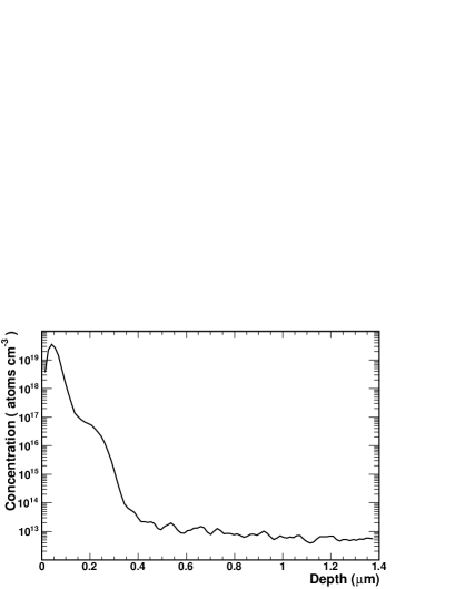
The thinned sensors are post-processed to create a thin entrance window on the back-plane and anneal the crystal damage from the thinning. A thin Phosphor layer contact is implanted at 33 keV using a cold process at -160∘C. The dose is adjusted to obtain an amorphous layer of Si, which favours crystal re-growth. After P implant the chip is annealed at 500∘C for ten minutes in Nitrogen atmosphere. The thickness of the P implantation is measured using spreading resistance analysis (SRA) on a chip. The result is shown in Figure 1 and indicates that the P implant extends to a depth of 0.4 m from the back-plane surface, with the highest concentration in the first 0.2 m.
This process provides the sensors with a thin entrance window on the back-plane ensuring in principle good sensitivity to X-rays down to 1.5 keV and to electrons down to 9 keV. After back-plane post-processing the leakage current is reduced to values comparable to, or lower than, those obtained on un-processed chips [6] and the sensors are functional with a total single pixel noise of (956) ENC, which is consistent with that of (838) measured on thick, un-processed sensors, and can be fully depleted.
3 Experimental set-up and results
The data acquisition of the SOI sensor is performed with the setup discussed in [4, 9]. Most of the measurements reported here have been performed with the chip clocked at 6.25 MHz, corresponding to a read-out time of 160 ns per pixel. Data sparsification is performed on-line in the DAQ PC using a custom Root-based [10] program. The matrix of pedestal subtracted data is scanned for seed pixels with signal exceeding a preset threshold in noise units. For each seed, the 77 pixel matrix centred around the seed position is selected and stored on file. Signal clusters are reconstructed offline by applying a double threshold method on the matrix of pixels selected around a candidate cluster seed. Clusters are required to have a seed pixel with a signal-to-noise ratio, S/N, of at least 5.0 and the neighbouring pixels with a S/N in excess of 2.5.
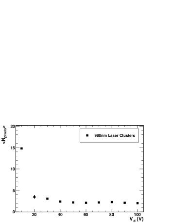
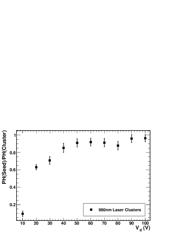
First the sensor is tested in the laboratory using 2 ns-long pulses of a 980 nm laser collimated to a 5 m spot on the pixel back-plane. The number of pixels accepted in a cluster, , and the ratio of the signal on the seed pixel to the total signal in the cluster measure the spread of the signal charge and the inter-pixel coupling. Figure 2 shows the pixel multiplicity in the clusters and the ratio of the signal on the seed pixel to the total signal in the cluster as a function of . The thinned sensor becomes fully depleted at 40 V. We observe that both the pixel multiplicity in the clusters, , and the ratio of the seed to cluster charge, , approach a plateau with average values of = 2.160.03 and = 0.930.01, above 40 V. The full depletion value is confirmed by curves [6].
|
The quantum efficiency for X-rays is studied on data collected at the beam-line 5.3.1 of the Advanced Light Source (ALS) at LBNL for various values of the photon energy and sensor depletion voltage . The thin, post-processed SOI sensor has been exposed to fluorescence radiation excited in various metal foils, with energy in the range 2.18.6 keV. The synchrotron radiation beam from a bending magnet is selected in energy through a monochromator to obtain a 12 keV monochromatic beam. This beam is sent on a target metal foil at a 45∘ incidence angle. A computer-controlled movable stage holds multiple foils, making possible to select different target materials remotely. The target and the detector are placed into a vacuum enclosure in order to minimise the absorption of soft X-rays in air at the lower energies (below 4 keV) and mounted in back-illumination configuration. The angle between the beam and the SOI sensor is 90∘. The energy spectrum and the fluorescence radiation intensity are monitored using a spectrometer consisting of a Si drift detector [11] with a FWHM resolution of 130 eV at 5.9 keV. This is installed at a 30∘ angle w.r.t. the incoming beam. The elements used as targets and the energies of their dominant fluorescence emission are given in Table 1.
 |
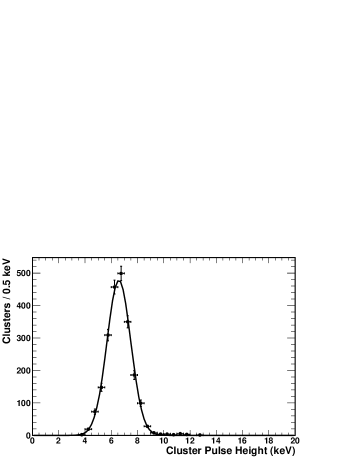 |
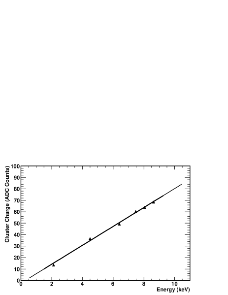
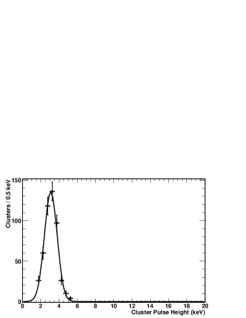
The ADC counts-to-energy conversion is determined from the position of the centroid of the full energy peak for X-rays of these energies. We estimate the charge-to-voltage conversion from the slope of the linear fit and obtain a calibration of (31.30.4) ADC count-1 at 50 V, consistent with the value obtained for a thick, unprocessed sensor of (29.91.2) ADC count-1 [4], and (33.30.4) ADC count-1 at 70 V. The calibration at = 70 V is shown in Figure 3. Due to charge diffusion and inter-pixel coupling the signal spreads on several pixels. In the energy range of interest for this study, the signal cluster size, , varies from 2.02 at 2.98 keV to 3.15 at 8.05 keV as the increasing energy deposit increases the likelihood for neighbouring pixels, sharing a constant fraction of the total deposited charge, to be above the threshold of 2.5 used in the cluster reconstruction. In order to improve the energy resolution for signal clusters with different pixel multiplicity, the energy calibration is performed separately for each value of multiplicity 15. The resulting spectra for Ag and Fe fluorescence are shown in Figure 4. Over the X-ray energy considered, we observe a Gaussian width of the full energy peak evolving from 700 eV at 3 keV to 1.14 keV at 8 keV, which is consistent with that expected from the measured pixel noise and multiplicity.
| Element | E (keV) |
|---|---|
| Au | 2.12 |
| Ag | 2.98 |
| Ti | 4.50 |
| Fe | 6.40 |
| Ni | 7.47 |
| Cu | 8.05 |
| Zn | 8.60 |
The detector quantum efficiency is measured by comparing the number of clusters detected within the full energy peak with the rate recorded on the spectrometer. Corrections are applied for the different solid angle, X-ray absorption and live exposure times of the SOI sensor and the spectrometer. The effect of the thickness of the active volume and window of the spectrometer is corrected using the manufacturer specifications. The efficiency of the SOI sensor depends on the product of X-ray absorption in the sensitive thickness and the transmission through the back-plane entrance window. We measure the total thickness of the thinned detector, (732) m, and estimate the total thickness of the top passivation, the CMOS and the buried oxide layers, to be 9 m, from manufacturer data. Then, we compute the depletion thickness of the handle wafer assuming the nominal resistivity value of 700 cm, which is consistent with the value of (753 73) cm determined from the charge collected for minimum ionising particles as a function of the depletion voltage [4]. The sensor is fully depleted for the voltages used. The thickness of the entrance window, , is left as a free parameter and extracted from the data by a fit.
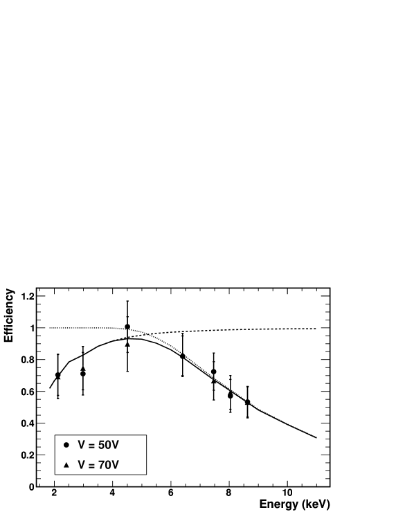
The back-illuminated thin SOI sensor response to X-rays is studied as a function of the photon energy and depletion voltage by comparing the rate of reconstructed clusters, compatible with the full energy peak, to the corrected rate recorded on the Si drift spectrometer.
Results are summarised in Figure 5, where the efficiency of the back-illuminated SOI pixel sensor, at values of corresponding to full depletion and over depletion, is compared to the expected Si absorption efficiency and entrance window transmission. The error bars include the statistical uncertainties as well as the systematics coming from the system geometry. The systematic uncertainties are correlated for the various energies and voltages. We extract the value of the back-plane window thickness in units of equivalent Si thickness by a 1-parameter fit to the data and obtain =(0.60.2) m, where the quoted error accounts for the statistical and systematic uncertainties on the data points. This value is in fair agreement with that of the P implant depth of 0.4 m obtained from the SRA analysis of the post-processed chip (see Figure 1). These results show that the post-processed, fully depleted SOI sensor operates with efficiency in excess of 0.60 for X-rays in the range 28 keV. For specific applications, the efficiency can be increased in the higher energy end of the spectrum by adopting a higher resistivity handle wafer. Recently, pixels have been manufactured on Float Zone (FZ) SOI wafers with resistivity of several 1000 cm, which can achieve full depletion over a thickness up to 500 m.
4 Potential Applications
The availability of a pixellated sensor with large quantum efficiency for soft X-rays and low-energy electrons, small pixels, fast readout and moderate energy resolution opens up a broad field of potential imaging applications. A first domain of possible applications is in precision beam monitoring in linacs and storage rings with X-rays and soft electrons. X-ray beam imaging for profile monitoring in low emittance electron storage rings such as synchrotron light sources and damping rings has been demonstrated [12, 13] and it requires a fast detector, sensitive to X-rays of a few keV, to minimise diffraction effects, and with small point spread function, to minimise resolution effects. Real-time quality control in hadrontherapy requires non-destructive position measurements of beams, which can be performed using secondary electron emission [14]. In this design the electron beam is accelerated to 20 keV and focused onto an imaging detector, for which a post-processed SOI sensor can be an interesting solution. Another field where a fully depleted, back-illuminated SOI sensor can be applied to image low-energy electrons is in transmission electron microscopy (TEM). Since the displacement damage threshold is proportional to , it is advantageous to use a low energy beam for the study of single atomic layers of carbon in graphene or carbon nano-tubes and in biology. In both applications, since the range of 20-40 keV electrons in Si is below 10 m, the contribution of multiple scattering in the sensor to the point spread function (PSF) is expected to be small. A study of PSF in TEM with a front-illuminated CMOS pixel sensor showed that the PSF tends to decrease for electron energies below 120 keV, since the decrease of the electron range limits the distance over which charge can be deposited [15]. The use of a back-illuminated SOI sensor for low energy TEM has a two-fold advantage. First, the amount of passive material traversed by the electron is much reduced compared to front illumination, 0.5 m compared to 4 m. Second, the radiation damage by the electron beam is greatly reduced, since electrons are stopped in the handle wafer without reaching the oxide and the CMOS layers. A detailed simulation study based on Geant-4 for the TEM application shows that the PSF for 20 keV electrons and back-illumination on a thin SOI sensors is comparable to that obtained with 300 keV electrons.
5 Conclusions
A pixel sensor in SOI technology on high-resistivity substrate thinned to 70 m to enable full depletion and implanted on the back-plane with a thin Phosphor contact, has been characterised with soft X-rays. Its response is evaluated in back-illumination using fluorescence radiation in the energy range of 2.12 up to 8.6 keV at the LBNL Advanced Light Source. After thinning and back-plane implant the pixel noise and conversion gain are measured and found to be consistent to those of sensors before post-processing. Over the X-ray energy range considered, the sensor showed an efficiency in excess of 60%, consistent with the expectations from photoabsorption in Si and transmission through the entrance window. The measured quantum efficiency curve is in agreement to that for a sensor with a (0.60.2) m back-plane passive window, in units of equivalent Si thickness.
Acknowledgements
This work is supported by the Director, Office of Science, of the U.S. Department of Energy under Contract No.DE-AC02-05CH11231 and by INFN, Italy. We are grateful to Y. Arai for his effective collaboration and support in the SOIPIX activities.
References
- [1] M. Battaglia et al., Nucl. Instr. and Meth. A 583 (2007) 526.
- [2] Y. Arai et al., Nucl. Instr. and Meth. A 623 (2010) 186.
- [3] Y. Arai et al., Nucl. Instr. and Meth. A 636 (2010) S237.
- [4] M. Battaglia et al., Nucl. Instr. and Meth. A 654 (2011) 258.
- [5] S.G. Ryu et al., IEEE Trans. on Nucl. Sci. 58 (5) (2011) 2528.
- [6] M. Battaglia et al., to be submitted to Nucl. Instr. and Meth. A.
- [7] Aptek Industries Inc. San Jose, CA 95111 USA.
- [8] M. Battaglia et al., Nucl. Instr. and Meth. A 579 (2007) 675.
- [9] M. Battaglia et al., Nucl. Instr. and Meth. A 611 (2009) 105.
- [10] R. Brun and F. Rademakers, Nucl. Instr. Meth. A 389 (1997) 81.
- [11] Amptek Inc., Bedford, MA 01730 USA, model X-123SDD.
- [12] K. Iida et al., Nucl. Instr. and Meth. A 506 (2003) 341.
- [13] S. Takano et al., Nucl. Instr. and Meth. A 556 (2006) 357.
- [14] M. Caccia et al., Nucl. Instr. and Meth. A 560 (2006) 153.
- [15] M. Battaglia et al., Nucl. Instr. and Meth. A 605 (2009) 350.