Electronic band gap and transport in Fibonacci quasi-periodic graphene superlattice
Abstract
We investigate electronic band gap and transport in Fibonacci quasi-periodic graphene superlattice. It is found that such structure can possess a zero- gap which exists in all Fibonacci sequences. Different from Bragg gap, zero- gap associated with Dirac point is less sensitive to the incidence angle and lattice constants. The defect mode appeared inside the zero- gap has a great effect on transmission, conductance and shot noise, which can be applicable to control the electron transport.
Graphene, a monolayer of carbon atoms tightly packed into a honeycomb lattice, has attracted great interest in graphene-based nanoelectronic and optoelectronic devices Castro , since it was fabricated by Novoselov and Geim et al. in 2004 Novoselov . In graphene, the unique band structure with the valance and conduction bands touching at Dirac point (DP) leads to the fact that electrons around the Fermi level can be described as the massless relativistic Dirac electrons, resulting in the linear energy dispersion relation. As a consequence, there are a great number of electronic properties, such as the half-integer quantum Hall effect Novoselov-GMJK ; Zhang-TS ; Gusynin-S , the minimum conductivity Novoselov-GMJK , and Klein tunneling Katsnelson-NG . In particular, Klein tunneling and perfect transmission are crucial for electron transport in various graphene heterostructures Young , i.e. single barrier Chen-APL and n-p-n junctions Cheianov .
Motivated by the experimental realization of graphene superlattice (GSL) Meye ; Marchini ; Vazquez , electronic bandgap structures and transport properties in GSLs with electrostatic potential and magnetic barrier have been extensively investigated Bai ; Barbier2009 ; Brey ; Park2008 ; Wang2010 ; YuXian ; Abedpour ; Bliokh ; Mukhopadhyay ; Sena , since the conventional semiconductor superlattices are successful in controlling the electronic structures and the extension to graphene may give rise to different features and applications. For instance, DP appears in the GSL Barbier2009 ; Brey , and it is exactly located at the energy with the zero- gap Wang2010 . Interestingly, the zero- gap associated with DP is insensitive to the lattice parameter changes in contrast with the behavior exhibited by Bragg gaps Wang2010 . This gap is analogous to photonic zero- gap in the photonic crystals containing negative-index and positive-index materials Bliokh , and originates from a zero total phase Li-PRL . Accordingly, the zero- gap is robust against the lattice constants, structural disorder Wang2010 , and external magnetic field YuXian , and thus is better to control the electron transport in GSL.
In this Letter, we will investigate electronic band gap and transport in Fibonacci quasi-periodic GSLs in the fashion analogous to photonic crystal with metamaterials Li-PRL ; Alfonoso ; Zhang . As we know, the quasi-periodic GSL is classified as intermediate between ordered and disordered systems Abedpour ; Bliokh , which has significant and common features like fractal spectrum and self-similar behavior Mukhopadhyay ; Sena . However, what we concentrate on here is the electronic band gap and DP in such quasi-periodic system. We find that zero- gap happens in all Fibonacci sequences, which results in the robust transmission properties, conductance and shot noise at the DP.
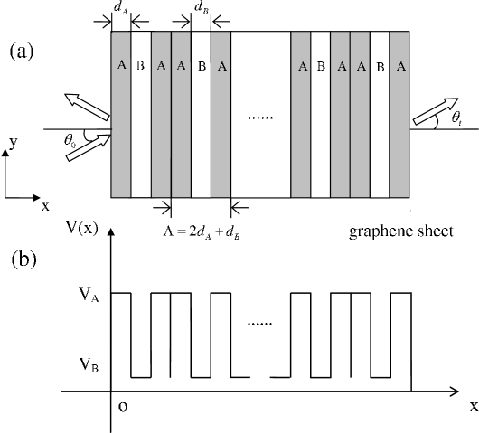
Consider quasi-periodic monolayer GSLs with the structure in each cell following the Fibonacci sequence, , by a recurrent relation , with and with is the generation number of the Fibonacci unit cell, the first few sequences are , , and so on. Elements and are considered as the alternating barriers and wells with the width and , respectively. As an example, the third-generation Fibonacci structure with the number of periods, , is shown in Fig. 1. Generally, in the vicinity of the point and in the presence of a potential , the charge carriers are described by the Dirac-like equation, where the Fermi velocity m/s, and are the Pauli matrices. Due to the translation invariance in the direction, the solution of above equation for a given incident energy and potential barrier can be presented as with
where , and are the and components of wavevector, for , otherwise , and () is the amplitude of the forward (backward) propagating wave. The wave functions at any two positions and inside the th potential can be related via the transfer matrix Wang2010 :
| (1) |
with . As a result, the transmission coefficient is found to be
| (2) |
where and are incidence and exit angles (see Fig. 1), and is the matrix element of total transfer matrix, , connecting the incident and exit ends, and is the total number of layers of the graphene superlattice. Once the transmission coefficient is obtained, the total conductance of the system at zero temperature is given as follows, Datta , where and and is the width of the graphene stripe in the direction. Meanwhile, the Fano factor is given by Beenakker-PRL .
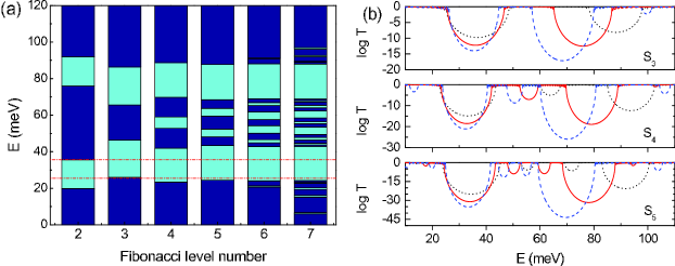
Fig. 2 shows the energy bands and transmission spectrum in various Fibonacci quasi-periodic GSLs (i.e., from to ). Besides the distribution of energy bands like Cantor-like set Sena , what we have discovered here is that the zero- gaps exist in all Fibonacci levels. In Fig. 2 (a), there are several broad forbidden gaps opened for each Fibonacci level in the considered energy range. Among these forbidden gaps, we notice that the position and size of zero- gaps are almost robust against the Fibonacci levels. In fact, the Fibonacci structure is exactly the GSL, . The condition for zero- gap is given by at , which provides the DP, , for the special case of and Wang2010 . For the higher Fibonacci level to , the zero- gaps become stabilized with the fixed position and size, although the location of zero- gaps is slightly different from that for Fibonacci level . Furthermore, we demonstrate, in Fig. 2 (b), that such gap depends only on the ratio of lattice constants, and is insensitive to the lattice parameters. On the contrary, the position and size of Bragg gaps in a higher energy range change sensitively with the Fibonacci level and lattice parameters.
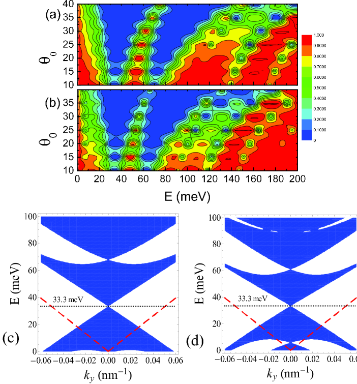
Fig. 3 (a) and (b) further display the influences of the incidence angle on the transmission spectrum in the Fibonacci quasi-periodic GSL, , corresponding to Fibonacci sequence . It is apparent that the zero- gap is independent of the lattice constants and is weakly dependent on the incidence angle. To understand better, the electronic dispersion at any incidence angle, based on the Bloch’s theorem, is written as,
| (3) | |||||
where is the length of the unit cell. Therefore, the location of the DP is given by at . For the structure considered here, ( and ), the DP is exactly located at , which means that the zero- gap depends only on the ratio, , instead of and themselves. Fig. 3 (c) and (d) show that a band gap opens at meV, which is different from meV for Fibonacci sequence , in which and meV. In fact, DP for other Fibonacci sequences can be further calculated as , where is the ratio of numbers of layer and , and .
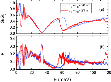
Fig. 4 shows the conductance and the Fano factor with the difference lattice constants. Remarkably, the angular-averaged conductance reaches the minimum value at the DP, while the Fano factor exists a peak in the vicinity of DP with value approximately Beenakker-PRL ; YuXian . The conductance and the Fano factor shows the robust properties, since the DP does not shift, when the lattice constants and are changed simultaneously.
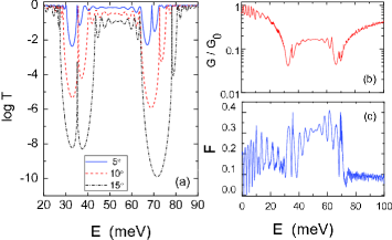
In Fig. 5, we further shed light on the effect of localized defect mode in GSL, , where the defect layer with nm and meV. Compared to that inside the Bragg gap, the defect mode inside the zero- gap remains almost invariant with the incidence angles and lattice constants. Due to the existence of the defect mode, the conductance is greatly enhanced, while the Fano factor is strongly suppressed, as shown in Fig. 5. This suggests that the electron transport can be modulated by the defect mode.
In summary, using the transfer matrix method, we have investigated the electronic band gap and transport in the Fibonacci quasi-periodic GSL. It is shown that the zero- gap and the defect mode are robust against the lattice constants and incidence angle, which is useful to control electron transport. We hope such Fibonacci structure will have applications in graphene-based electronic omnidirectional reflector and filters.
This work was supported by the NSFC (Grant Nos. 60806041 and 61176118), and the Shanghai Leading Academic Discipline Program (Grant No. S30105). X. C. also acknowledges Juan de la Cierva Programme, the Basque Government (Grant No. IT472-10) and MICINN (Grant No. FIS2009-12773-C02-01).
References
- (1) A. H. Castro Neto, F. Guinea, N. M. R. Peres, K. S. Novoselov, A. K. Geim, Rev. Mod. Phys. 81, 109 (2009).
- (2) K. S. Novoselov, A. K. Geim, S. V. Morozov, D. Jiang, Y. Zhang, S. V. Dubonos, I. V. Grigorieva, A. A. Firsov, Science 306, 666 (2004).
- (3) K. S. Novoselov, A. K. Geim, S. V. Morozov, D. Jiang, M. I. Katsnelson, I. V. Grigorieva, S. V. Dubonons, and A. A. Firsov, Nature (London) 438, 197 (2005).
- (4) Y. Zhang Y. W. Tan, H. L. Stromer, and P. Kim, Nature (London) 438, 201 (2005).
- (5) V. P. Gusynin, and S. G. Shararpov, Phys. Rev. Lett. 95, 146801 (2005).
- (6) M. I. Katsnelson, K. S. Novoselov, and A. K. Geim, Nat. Phys. 2, 620 (2006).
- (7) A. F. Young and P. Kim, Annu. Rev. Condens. Matter Phys. 2, 101 (2011).
- (8) X. Chen and J.-W. Tao, Appl. Phys. Lett. 94, 262102 (2009).
- (9) V. V. Cheianov and V. I. Fal’ko, Phys. Rev. B 74, 041403(R) (2006).
- (10) J. C. Meyer, C. O. Girit, M. F. Crommie, and A. Zettl, Appl. Phys. Lett. 92, 123110 (2008).
- (11) S. Marchini, S. Günther, and J. Wintterlin, Phys. Rev. B 76, 075429 (2007).
- (12) A. L. Vazquez de Parga, F. Calleja, B. Borca, M. C. G. Passeggi, Jr., J. J. Hinarejos, F. Guinea, and R. Miranda, Phys. Rev. Lett. 100, 056807 (2008).
- (13) C.-X. Bai and X.-D. Zhang, Phys. Rev. B 76, 075430 (2007).
- (14) M. Barbier, F. M. Peeters, and P. Vasilopoulos, Phys. Rev. B 80, 205415 (2009); 81, 075438 (2010).
- (15) L. Brey and H. A. Fertig, Phys. Rev. Lett. 103, 046809 (2009).
- (16) C. H. Park, L. Yang, Y. W. Son, M. L. Cohen, and S. G. Louie, Phys. Rev. Lett. 101, 126804 (2008).
- (17) L.-G. Wang and S.-Y. Zhu, Phys. Rev. B 81, 205444 (2010); L.-G. Wang and X. Chen, J. Appl. Phys. 109, 033710 (2011).
- (18) X.-X. Guo, D. Liu, and Y.-X. Li, Appl. Phys. Lett. 98, 242101 (2011).
- (19) N. Abedpour, A. Esmailpour, R. Asgari, and M. R. R. Tabar, Phys. Rev. B 79, 165412 (2009).
- (20) Y. P. Bliokh, V. Freilikher, S. Savel’ev, and F. Nori, Phys. Rev. B 79, 075123 (2009).
- (21) S. Mukhopadhyay, R. Biswas, and C. Sinha, Phys. Status. Solidi (b) 247, 342 (2009).
- (22) S. H. R. Sena, J. M. Pereira Jr, G. A. Farias, M. S. Vasconcelos, and E. L. Albuquerque, J. Phys.: Condens. Matter. 22, 465305 (2010).
- (23) J. Li, L. Zhou, C. T. Chan, and P. Sheng, Phys. Rev. Lett. 90, 083901 (2003).
- (24) A. Bruno-Alfonoso, E. Reyes-Gómez, S. B. Cavalcanti, and L. E. Oliveira, Phys. Rev. A 78, 035801 (2008).
- (25) L.-W. Zhang, K. Fang, G.-Q. Du, H.-T. Jiang, and J.-F. Zhao, Opt. Commun. 284, 703 (2011).
- (26) S. Datta, Electronic Transport in Mesoscopic Systems (Cambridge University Press, Cambridge, England, 1995).
- (27) J. Tworzydło, B. Trauzettel. M. Titov, A. Rycerz, and C. W. J. Beenakker, Phys. Rev. Lett. 96, 246802 (2006).