Effects of scattering area shape on spin conductance in a four-terminal spin-Hall setup
Abstract
We study spin conductance in a ballistic and quasi-ballistic two dimensional electron system with Rasbha spin-orbit coupling. The system has a four-terminal geometry with round corners at the connection to the leads. It is found that by going from sharp corners to more round corners in the ballistic system the energy depended spin conductance goes from being relatively flat to a curve showing a series of minima and maxima. It is also found that when changing the size of the terminal area by modifying the roundness of the terminal corners the maxima and minima in the transverse spin conductance are shifted in energy. This shift is due increased (decreased) energy for smaller (larger) terminal area. These results were also found to be reasonably stable in quasi-ballistic systems.
pacs:
72.25.Dc, 71.70.Ej, 85.75.-d, 73.23.Ad, 72.20.DpI Introduction and motivation
Spin-orbit (SO) coupling in semiconductor nanostructures has for some time been considered as one of the main candidates in controlling spin in semiconductor spintronic devices Wolf et al. (2001); Awschalom et al. (2002); Awschalom and Flatte (2007). One of the main benefits of the SO coupling is that it can be used to manipulate electron spins in semiconductors through gate voltages instead of external magnetic fieldsPrinz (1998) or magnetic dopingDietl (1994). SO coupling arises from relativistic effects and when combined with - calculation it will lead to spin-orbit terms depending on the crystal structure, i.e. the Dresselhaus SO couplingDresselhaus (1955); Winkler (2010) in crystals that lack inversion symmetry. In addition, further spin-orbit contributions can occur at heterostructure interfaces. This contribution is the so-called Rashba SO couplingRashba (1960); Winkler (2010). Voltages applied to local gates can change the heterostructure confining potential, thus modifying the Rashba SO couplingNitta et al. (1997); Schapers et al. (2009). More recently, yet a new type of spin-orbit interaction has been found in symmetric two-dimensional quantum structures with two subbands: the inter-subband induced spin-orbit couplingBernardes et al. (2007); Calsaverini et al. (2008).
In the field of spintronics the main goals is the creation and detection of spin-currents. In electron doped semiconductor structures one of the main candidates for spin-current creation is the so-called spin-Hall effectSinova et al. (2004). Although it has been proved that in extended 2D systems the spin-Hall effect vanishes Inoue et al. (2004); Chalaev and Loss (2005); Erlingsson et al. (2005), this results does not hold in finite size systems. The exception here are systems with the inter-subband induced spin-orbit couplingBernardes et al. (2007); Calsaverini et al. (2008), which gives rise to a non-zero spin Hall effectLee et al. (2009), even for extended systems. The interplay of in-plane confinement and spin-orbit interaction leads to many interesting spin-related transport phenomena.
The Rashba SO coupling has been in recent years extensively studied both experimentally Miller et al. (2003); Schäpers et al. (2004); Kato et al. (2004); Sih et al. (2005, 2006); Schapers et al. (2009); Debray et al. (2009) and theoretically, either in two-terminal setups, Reynoso et al. (2006); Zhang et al. (2005); Nikolić and Souma (2005); Nikolić et al. (2005a, b); Duckheim et al. (2010), or in multiterminal setups Garelli and Schliemann (2009); Xing et al. (2006); Yokoyama and Eto (2009); Yamamoto et al. (2005); Nikolić et al. (2005a, c). Previous numerical studies hint that the shape of the scattering area of the system plays a vital role in the behavior of the spin current flowing through the transverse leads Xing et al. (2006); Yokoyama and Eto (2009). Also one expects that gate defined nanostructures will have confinement potential that changes on a length scale much larger than the Fermi wavelength of the electronsIhn (2010).
In this work we will present calculation of spin conductance through transverse leads in a four terminal spin Hall setup where the shape of the scattering region is changed. Most lattice model calculationsGarelli and Schliemann (2009); Xing et al. (2006); Yokoyama and Eto (2009); Yamamoto et al. (2005); Nikolić et al. (2005a, c) used abrupt edges in the way the leads where connected to the scattering region. This abruptness leads to substantial scattering (both of charge and spin) which can suppress spin-related phenomena that one is interested in. We use smooth connection of leads to the scattering area. Since most semiconductor heterostructures are defined by gates, one would expect relatively smooth confining potentials Ihn (2010). We study the spin conductance as a function of scattering area shape and propose an explanation of the observed connection between the spin conductance and the change of size of the scattering region. We also observe that the values of spin conductance is relatively large which is due to the smooth transfer of electrons from the longitudinal leads to the transverse one.
The paper is organized as follows. In section II we present the theory behind the calculations. Section III defines the parameters used in the calculations and presents the results for the ballistic system in subsection A and for the quasi-ballistic system in subsection B. Finally section IV contains conclusions and discussion.
II Theory
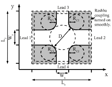
We are interested in a four terminal 2DEG in a semiconductor heterostructure. A schematic of the scattering region of the system can be seen in Fig. 1. The system is described by the following effective mass Hamiltonian
| (1) |
where is the effective electron mass. describes a hard-wall confining potential shape of the four terminal junction with round corners. The roundness of each corner can be controlled independently by varying the radii of the circular corners, and .
In a region centered on the scattering area we have a SO coupling which is described by the symmetrized Rashba Hamiltonian
| (2) |
Here is the Rashba SO coupling strength which is turned on smoothly at the edges of the scattering region. Having Rashba SO coupling only in a finite area of the sample can be achieved by using metallic gate on top of the 2DEG Engels et al. (1997). The Hamiltonian is discretized on a square lattice using the finite difference method, resulting in an infinitely large matrix. The corresponding matrix equation for the retarded Green’s function matrix of the system is
| (3) |
The scattering region part of the Hamiltonian Eq. (3) can be made finite by treating the leads as self-energies in the standard way Datta (1995); Ferry and Goodnick (1997). The leads have no SO coupling. The finite version of the matrix equation is
| (4) |
Here the self-energy of lead is , is the Hamiltonian of the scattering region and is the retarded Green’s function. All the matrices are matrices. In order to save computational power only the necessary Green’s function matrix elements are calculated with the recursive Green’s function method Ferry and Goodnick (1997). From the Green’s functions both the spin conductance and spin-densities can be calculated. The spin density for an bias of is
| (5) |
where is the Pauli matrix for the direction,
| (6) |
is the lesser Green’s functionHaug and Jauho (2008), , and is the Fermi function in lead which has the chemical potential . We define the spin-dependent conductance between the leads and as
| (7) |
Using the Landauer Büttiker formula we write the linear response of the spin depended current through lead as
| (8) |
III Numerical simulations
The dimension of the scattering area is set within a box shaped area, where nm. This area is discretized on a point grid with constant mesh size nm and the effective electron mass is set as , which is a reasonable value for Ga1-xInxAs alloysA. and Schmidt (1996). In the simulations all lengths where scaled in the mesh size and energies in the tight-binding hopping term meV which results from the finite difference discretization of the Hamiltonian in Eq. (1). Four leads connect to the system, two main leads with width nm (leads 1 and 2) and two transverse leads with width nm (leads 3 and 4). In the following, the energy will be scaled in the lowest transverse energy of the main leads, meVt. Similarly we also define which is the lowest transverse energy of the transverse leads. The effect of Rashba SO coupling is turned on smoothly over a nm strip at the edge of the scattering area, see the hatched area in Fig. 1, to its full strength . Between the two main leads we apply a bias . This means that the chemical potentials at the leads measured from will be , and . According to Eq. (8) the spin depended current () is then
| (9) |
We define the spin Hall conductance in transverse lead as
| (10) |
Note that in our scenario the total charge current through the transverse leads is always zero because of how we define the bias over the leads. Throughout the paper the full strength of the Rasbha SO coupling will be set as meV nm, where . This value of Rashba SO coupling is typical for Ga1-xInxAs alloys and is also in the regime where we begin to see strong and interesting features in spin conductance through the transverse lead.
III.1 Ballistic system
We will start by showing the spin Hall conductance through the transverse leads in a clean system. In Fig. 2 the spin Hall conductance through lead 3, , is plotted as a function of Fermi energy for three types of shapes. Fig. 2 a) corresponds to shape with , Fig. 2 b) to . In both figures the the spin conductance for a sharp corner system () is plotted for comparison. Here we use when all the corners have the same curvature.
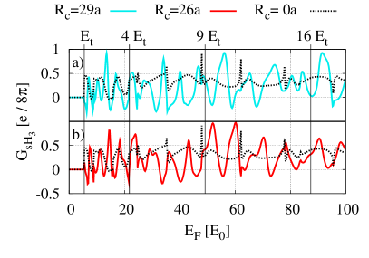
In Fig. 2 a) and b) we see that the spin conductance curves corresponding to the round corner system shows a series of minima and maxima. These extrema are most likely related to the resonance states in the scattering area which we will discuss below.
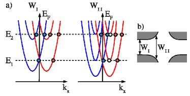
The resonance states form when the leads get adiabatically larger which results in a downward shift in the transverse energy bands of the leadsBaranger et al. (1991), see Fig. 3. This causes new states to become available at the Fermi energy which have very low longitudinal velocity (). Near the transverse leads the adiabatic approximation ceases to apply and the electron scatter in to different states, including the newly opened low longitudinal velocity states which give rise to conductance extrema in the transverse leads.
The sharp corner curve, shown both in Fig. 2 a) and b), behaves differently. At high enough energies () the curve changes slowly with energy and has no significant resonance peaks, apart from isolated peaks due to divergence in the density of states at energies corresponding to the band bottom in the longitudinal leads. The observed behaviour of the sharp corner is due to the strong scattering by the sharp corners. An electron coming in from the left, with a definite -value, gets scattered into all possible states, with the same energy, when it enters the scattering region. For higher energies these states are many, all corresponding to different effective magnetic fields which tend to average out the spin-signal. Note that for low energies we still see peaks and minima since only a few -states are available at such low energies.
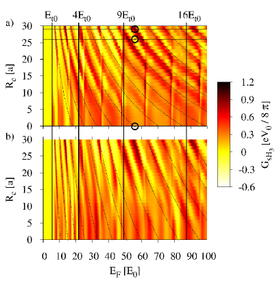
Comparing the round corner curves in Fig. 2 a) and b) we see that the extrema at in Fig. 2 a) has shifted to in Fig. 2 b). Other extrema in seem also to have been shifted by the change in corner radius . To explore in more detail this shift of extrema in with change in curvature we make a surface plot of the spin Hall conductance through lead 3, , as a function of Fermi energy varied from to and varied from (sharp corners) to with interval of . The result can be seen in Fig. 4 a). There we see that for low corner curvatures () the spin conductance becomes smeared out as was discussed above.
For higher corner curvatures () we get a spin conductance curve which shows a series of minima and maxima. Extrema in also begin to shift in energy with increasing corner curvature. For smoother corners the transport gets more adiabatic and the extrema in will be more influenced by geometric resonances, i.e. changes in shape will be adiabatically translated into a shift in the energy bands, that will affect the transport. Changing the curvature of the scattering region effectively changes its area. For smooth enough corners,the shape of the system is not affected by changing the curvature, only its size, which results in a universal shift of all bands in the scattering area. This does not apply to the sharp corners, where a small change in curvature can results in great change in scattering properties.
The effective diameter of the scattering region is , see Fig. 1. The energy shift of a given extrema will be . The prefactor is not known, but this does not matter as we will show here below.
We can pick a reference energy , with reference size , on the same extrema in . By dividing with this reference energy we get rid of the unknown prefactor in and obtain
| (11) |
which describes the shift of the energy levels in the scattering area as a function of the shape of the scattering area.
In Fig. 4 a) we have plotted curves, shown with black dashed lines, with reference points at on all the spin conductance maxima. As can be seen for the shift of the maxima curves fits well to the shift that we expect for adiabatic change in size of the scattering area. For scattering from the corners gets more dominating, which is to be expected since the system is out the adiabatic regime and the sensitivity to the corners takes over.
A shape where we keep fixed and only vary was also examined, see Fig. 4 b). Here we also plot curves based on Eq. (11), shown with black dashed lines, with reference points at on all the maxima curves. We notice that the for low corner curvatures, , we get somewhat more structure than for low in the equal corner shape. This is due to that only two corners are contributing to the sharp corner scattering. We also notice that for the shift in spin conductance maxima follows the expected shift calcuated from Eq. (11).
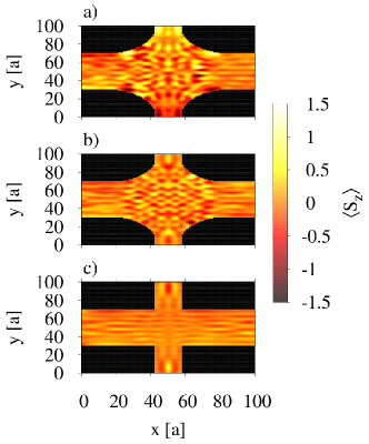
To examine the effect of corner curvature better we also plot the density of the spin component in the scattering region for three types of all equal corner shapes , see Fig. 5 a), , see Fig. 5 b), and , see Fig. 5 c). For all three types we set the bias as and temperature at .
In Fig. 5 a) we have stronger spin densities along the corner edges and within the transverse leads than in Fig. 5 b). Also the spin densities averaged over the transverse leads in Fig. 5 b) is lower compared to equivalent averaging in Fig. 5 a). These densities correspond to spin conductance strength marked with black circles in Fig. 4 a) and as expected the more negative spin conductance yields more negative spin density averaged over the transverse leads. For comparison we also include spin density in the sharp corner system, see Fig. 5 c). We see that the spin density in the sharp corner system is more smeared out than in the round corner systems, as could be expected in light of previous discussion about the sharp corner system. Note though that these spin densities seen in Fig. 5 are not large, only up to per nm2.
The results presented in this section suggest that polarization of the spin current through the transverse leads can be effectively controlled by tuning the curvature of the corners in the scattering area. This could be realised by using e.g. finger gatesLiang et al. (2004).
III.2 Quasi-ballistic system
To test how robust the extrema are, we add impurity effects to our model. Two different methods of including impurity effects were studied. The first method which we will consider involves adding a few randomly distributed Gaussian shaped impurities to the sample. The second method which we considered is the Anderson impurity method which has already been extensively used for similar simulations Anantram and Govindan (1998); Nikolić et al. (2005b, a); Garelli and Schliemann (2009); Anantram and Govindan (1998); Duckheim et al. (2010); Grincwajg et al. (1997).
III.2.1 Static impurities
Phenomena such as crystal defects can introduce extra potential bumps in the otherwise uniform potential background. These bumps can be described as static Gaussian shaped impurities in the scattering region which we add randomly to our scattering region via the term
| (12) |
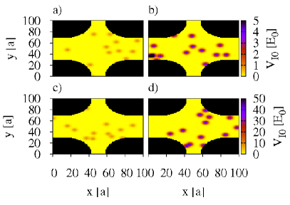
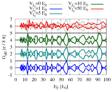
which is added to the Hamiltonian in Eq. (1). Here is the potential height of the potential bump, is the number of impurities, the center point of each impurity and impurity range. We would expect the number of these impurities to be just a few percent of the number of donors. We choose 2% which corresponds to roughly Gaussian impurities in an nm2 area and a delta donor density of cm-2. We are interested in seeing how strong these Gaussian shaped impurities must be to have significant effect on the spin hall conductance. To accomplish this four cases of impurity strength were studied: , , , and , see Fig. 6. These values of impurity strength are roughly the same order of magnitude as a screened and unscreened point charge 17 nm away from a 2DEG in Ga[Al]As heterostructureIhn (2010).
The effect these impurities have on the spin Hall conductance in leads 3 and 4 can be seen in Fig. 7. There we see that up to impurity strength the spin conductance is rather stable and that spin conductance through lead 3 and 4 is symmetric around zero.
III.2.2 Anderson type impurities
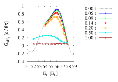
The Anderson impurity potential adds to each point in the scattering area a random value of potential energy in the range , where describes the disorder strength. To study the effect of the Anderson type impurities on we focus on a extrema in at for a scattering shape, see Fig. 2 a) . In Fig. 8 the spin Hall conductance is plotted for impurity strength ranging from to . Each data point is averaged over 1000 impurity configurations. For comparison we include the result for the ballistic system, seen also in Fig. 2 a). In Fig. 8 we see that the structure of the spin conductance is stable up to although its amplitude diminishes and the structure shifts with increasing disorder strength. For the spin conductance seems to be disappearing as has been shown for such large disorder valuesNikolić et al. (2005c).
IV Conclusions and discussion
In this paper the effect of scattering area shape on spin conductance in a four-terminal 2DEG structure with Rashba SO coupling is studied numerically. The change in the scattering region was implemented by modifying the curvature of the corners between different leads. Both the ballistic regime and the quasi-ballistic regime were considered. It is found that above a certain curvature the spin conductance, , shows a series of minima and maxima, as a function of energy. These minima and maxima are shifted in energy with increasing curvature. We propose a relation between this shift of the extrema and the change in the size of the scattering area when the curvature is increased. This is due to the increased energy for smaller scattering areas and describes the observed shift of the extrema reasonably well. With this relation the polarization of the spin current through the transverse leads could effectively be controlled by tuning the curvature of the corners in the scattering area.
In addition, we have also test the robustness of the spin conductance extrema by adding impurities to the scattering area. Static and Anderson type impurities were considered. The amplitude of the spin conductance extrema are suppressed with increasing impurity strength but the structure is shown to be stable under reasonable values of impurity strength, i.e. when the system is quasi-ballistic.
Acknowledgements.
We gratefully acknowledge helpful discussions with Mathias Dückheim and Andrei Manolescu. This work was supported by the Icelandic Science and Technology Research Program for Postgenomic Biomedicine, Nanoscience and Nanotechnology, the Icelandic Research Fund, and the Research Fund of the University of Iceland.References
- Wolf et al. (2001) S. A. Wolf, D. D. Awschalom, R. A. Buhrman, J. M. Daughton, S. von Molnar, M. L. Roukes, A. Y. Chtchelkanova, and D. M. Treger, Science 294, 1488 (2001).
- Awschalom et al. (2002) D. Awschalom, D. Loss, and N. Samarth, Semiconductor Spintronics and Quantum Computation (Springer, 2002).
- Awschalom and Flatte (2007) D. D. Awschalom and M. E. Flatte, Nat Phys 3, 153 (2007), ISSN 1745-2473.
- Prinz (1998) G. A. Prinz, Science 282, 1660 (1998).
- Dietl (1994) T. Dietl, Dilute magnetic semiconductors, vol. 3B of Materials, Properties and Preparation (Handbook on Semiconductors) (North Holland, Amsterdam, 1994).
- Dresselhaus (1955) G. Dresselhaus, Phys. Rev. 100, 580 (1955).
- Winkler (2010) R. Winkler, Spin-orbit Coupling Effects in Two-Dimensional Electron and Hole Systems (Springer Berlin Heidelberg, 2010).
- Rashba (1960) E. I. Rashba, Sov. Phys. Solid State 2, 1109 (1960).
- Nitta et al. (1997) J. Nitta, T. Akazaki, H. Takayanagi, and T. Enoki, Phys. Rev. Lett. 78, 1335 (1997).
- Schapers et al. (2009) T. Schapers, V. A. Guzenko, A. Bringer, M. Akabori, M. Hagedorn, and H. Hardtdegen, Semiconductor Science and Technology 24, 064001 (11pp) (2009).
- Bernardes et al. (2007) E. Bernardes, J. Schliemann, M. Lee, J. C. Egues, and D. Loss, Phys. Rev. Lett. 99, 076603 (2007).
- Calsaverini et al. (2008) R. S. Calsaverini, E. Bernardes, J. C. Egues, and D. Loss, Phys. Rev. B 78, 155313 (2008).
- Sinova et al. (2004) J. Sinova, D. Culcer, Q. Niu, N. A. Sinitsyn, T. Jungwirth, and A. H. MacDonald, Phys. Rev. Lett. 92, 126603 (2004).
- Inoue et al. (2004) J.-i. Inoue, G. E. W. Bauer, and L. W. Molenkamp, Phys. Rev. B 70, 041303 (2004).
- Chalaev and Loss (2005) O. Chalaev and D. Loss, Phys. Rev. B 71, 245318 (2005).
- Erlingsson et al. (2005) S. I. Erlingsson, J. Schliemann, and D. Loss, Phys. Rev. B 71, 035319 (2005).
- Lee et al. (2009) M. Lee, M. O. Hachiya, E. Bernardes, J. C. Egues, and D. Loss, Phys. Rev. B 80, 155314 (2009).
- Miller et al. (2003) J. B. Miller, D. M. Zumbühl, C. M. Marcus, Y. B. Lyanda-Geller, D. Goldhaber-Gordon, K. Campman, and A. C. Gossard, Phys. Rev. Lett. 90, 076807 (2003).
- Schäpers et al. (2004) T. Schäpers, J. Knobbe, and V. A. Guzenko, Phys. Rev. B 69, 235323 (2004).
- Kato et al. (2004) Y. K. Kato, R. C. Myers, A. C. Gossard, and D. D. Awschalom, Science 306, 1910 (2004).
- Sih et al. (2005) V. Sih, R. C. Myers, Y. K. Kato, W. H. Lau, A. C. Gossard, and D. D. Awschalom, Nat Phys 1, 31 (2005), ISSN 1745-2473.
- Sih et al. (2006) V. Sih, W. H. Lau, R. C. Myers, V. R. Horowitz, A. C. Gossard, and D. D. Awschalom, Phys. Rev. Lett. 97, 096605 (2006).
- Debray et al. (2009) P. Debray, S. M. S. Rahman, J. Wan, R. Newrock, M. Cahay, A. T. Ngo, S. E. Ulloa, S. Herbert, M. Muhammad, and M. Johnson, Nat Nano 4, 759 (2009), ISSN 1748-3387.
- Reynoso et al. (2006) A. Reynoso, G. Usaj, and C. A. Balseiro, Phys. Rev. B 73, 115342 (2006).
- Zhang et al. (2005) L. Zhang, P. Brusheim, and H. Q. Xu, Phys. Rev. B 72, 045347 (2005).
- Nikolić and Souma (2005) B. K. Nikolić and S. Souma, Phys. Rev. B 71, 195328 (2005).
- Nikolić et al. (2005a) B. K. Nikolić, S. Souma, L. P. Zârbo, and J. Sinova, Phys. Rev. Lett. 95, 046601 (2005a).
- Nikolić et al. (2005b) B. K. Nikolić, L. P. Zârbo, and S. Welack, Phys. Rev. B 72, 075335 (2005b).
- Duckheim et al. (2010) M. Duckheim, D. Loss, M. Scheid, K. Richter, I. Adagideli, and P. Jacquod, Phys. Rev. B 81, 085303 (2010).
- Garelli and Schliemann (2009) M. S. Garelli and J. Schliemann, Phys. Rev. B 80, 155321 (2009).
- Xing et al. (2006) Y. Xing, Q.-f. Sun, and J. Wang, Phys. Rev. B 73, 205339 (2006).
- Yokoyama and Eto (2009) T. Yokoyama and M. Eto, Phys. Rev. B 80, 125311 (2009).
- Yamamoto et al. (2005) M. Yamamoto, T. Ohtsuki, and B. Kramer, Phys. Rev. B 72, 115321 (2005).
- Nikolić et al. (2005c) B. K. Nikolić, L. P. Zârbo, and S. Souma, Phys. Rev. B 72, 075361 (2005c).
- Ihn (2010) T. Ihn, Semiconductor Nanostructures: Quantum states and electronic transport (Oxford University Press, 2010).
- Engels et al. (1997) G. Engels, J. Lange, T. Schäpers, and H. Lüth, Phys. Rev. B 55, R1958 (1997).
- Datta (1995) S. Datta, Electronic Transport in Mesoscopic Systems (Cambridge University Press, 1995).
- Ferry and Goodnick (1997) D. K. Ferry and S. M. Goodnick, Transport in Nanostructures (Cambridge University Press, 1997).
- Haug and Jauho (2008) H. J. W. Haug and A.-P. Jauho, Quantum Kinetics in Transport and Optics of Semiconductors: Second, Substantially Revised Edition (Springer Berlin Heidelberg, 2008).
- A. and Schmidt (1996) G. Y. A. and N. M. Schmidt, Handbook Series on Semiconductor Parameters, Volume 2, vol. 2 (World Scientific Publishing Company, 1996).
- Baranger et al. (1991) H. U. Baranger, D. P. DiVincenzo, R. A. Jalabert, and A. D. Stone, Phys. Rev. B 44, 10637 (1991).
- Liang et al. (2004) C.-T. Liang, O. A. Tkachenko, V. A. Tkachenko, D. G. Baksheyev, M. Y. Simmons, D. A. Ritchie, and M. Pepper, Phys. Rev. B 70, 195324 (2004).
- Anantram and Govindan (1998) M. P. Anantram and T. R. Govindan, Phys. Rev. B 58, 4882 (1998).
- Grincwajg et al. (1997) A. Grincwajg, G. Edwards, and D. K. Ferry, Journal of Physics: Condensed Matter 9, 673 (1997).