Selection rules for Raman-active electronic excitations in carbon nanotubes
Abstract
Raman measurements in carbon allotropes are generally associated with the exploration of the vibrational modes. Here, we present a theory of the non-resonant inelastic light scattering accompanied by the excitations of intersubband electron-hole pairs in carbon nanotubes and predict the selection rules and polarization properties of the dominant intersubband Raman active modes.
pacs:
73.63.Bd, 73.43.Cd, 81.05.U-Carbon nanotubes (CNTs) are one of the most exhaustively investigated allotropes of carbon dresselhaus . In particular, CNTs have been extensively studied using optical spectroscopy: absorption of light absorption1 ; absorption2 ; absorption3fluorescence2 ; absorption4 ; absorption5 , fluorescence fluorescence1 ; absorption3fluorescence2 ; fluorescence3raman5 ; fluorescence4 ; fluorescence5 ; fluorescence6 , and inelastic (Raman) light scattering raman1 ; raman2 ; raman3 ; raman4 ; fluorescence3raman5 ; raman6 ; book-r . Absorption and luminescence studies of CNTs addressed the electron-hole excitations in a semiconductor nanotubes with small radii, Raman spectroscopy was effectively employed for characterizing vibrational modes. However, up to now, only one study raman7el has reported an observation interpreted as a double-resonant Raman inelastic scattering of light resulting in the creation of electronic excitation in CNTs. Moreover, no experiment or theory has been reported, yet, on the non-resonant Raman scattering with the e-h excitations in the final state, similar to those observed in graphene. In this Letter we offer a theory of inelastic light scattering in large-radius carbon nanotubes accompanied by the excitation of the low-energy electron-hole pairs in the final state of the non-resonant Raman process.
Theoretically, electronic properties of CNTs have a lot in common with those of graphene: a nanotube can be viewed as a rolled-up sheet of graphene. Recently, Raman spectroscopy of electronic excitations in graphene was understood theoretically erraman ; erraman2 and, then, realized experimentally erexp ; *erexp2. In contrast to a non-relativistic plasma of free electrons where inelastic scattering of light is dominated by the second-order contact interaction of charge carriers instantaneously with two photons platzmanwolff , in graphene it is dominated by a two-step process consisting of sequential events of single-photon absorption and emission, with a virtual state between them. This leads to the Raman spectrum transforming into a pronounced structure of inter-Landau-level excitons in an external magnetic field, with the strongest resonances at the energies equal to twice the Landau level energy of the Dirac electron erraman ; erraman2 ; erexp ; *erexp2.
To compare, a structure of Raman spectra in carbon nanotubes should be determined by the quantization of electronic states into quasi-one-dimensional subbands, with the characteristic van Hove singularities near the subband edges. Below, we determine the selection rules for the dominant Raman-active intersubband electron-hole excitations in CNTs, estimate their quantum efficiency, and find the relation between the polarizations of incoming and Raman-scattered photons.
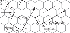
Using a close relation with graphene, illustrated in Fig. 1, electron states in a carbon nanotube characterized by chirality vector Note1 and diameter can be described as plain waves,
| (1) |
with momenta counted from the -points in the Brillouin zone of the honeycomb lattice. Here we use the basis for the () and for () valley, where are components of the wave functions defined on the () sublattice of the honeycomb lattice, and is the electron valley momentum along the nanotube axis. Integer stands for the quantum number characterizing the electron angular momentum around the nanotube, , and . Then, the CNT Hamiltonian reads dresselhaus
| (2) |
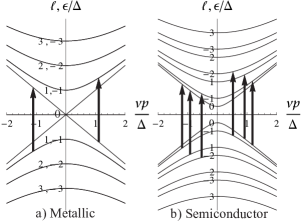
where is Dirac velocity in graphene, and , and Pauli matrices act in the space of spinors , and is a minimal remainder of division of by . The CTN spectrum (sketched in Fig. 2), with attributing states to the conduction () or valence () band,
| (3) |
can be metallic (), or semiconducting (). All armchair nanotubes are metallic, while chiral and zigzag nanotubes can be both metallic or semiconducting, depending on their diameter dresselhaus . All subbands in Eq. (3) are valley and spin degenerate.


This relation between graphene and CNTs can be also exploited to describe the electron interaction with light,
| (4) |
Here, one takes into account that a projection of the vector potential of the external electromagnetic field onto the unfolded sheet acquires periodic spatial dependence in its part perpendicular to the CNT axis,
| (5) |
The latter feature sets the selection rules ando for the interband transitions excited by the electromagnetic field (see Table 1): for polarized along the CNT axis () and for polarized perpendicular to the CNT axis (). These selection rules determine the dominant lines in the absorption absorption2 ; fluorescence1 ; fluorescence5 and luminescence fluorescence1 ; fluorescence3raman5 ; fluorescence5 spectra of long CNTs, where the processes with may be additionally enhanced by the antenna effect.
The electron-photon interaction in Eqs. (4,5) can be used to establish the selection rules for the inelastic scattering of photons from a large-radius CNT, with an electron-hole pair left in the final state at the excitation energy , where is the energy of incoming photon. In 2D graphene, the main contribution to the amplitude of inelastic light scattering is given by two Feynman diagrams,
| (6) |
describing sequential absorption and emission of individual photons, one corresponding to the absorption event preceding emission with a large excess of energy in the intermediate state, and the other with emission preceding absorption and energy deficit in the intermediate state. In these Feynman diagrams, thin straight lines identify electrons in the “in” and “out” states with the energies and , wavy lines — absorbed and emitted field and . The thick line in is the electron propagator in the intermediate state, for the first diagram and for the second, where is the Raman shift, and the sum is taken over the intermediate electron states with energies . For the case of studied here, one can approximate . This approximation enables us to simplify the expression for the effective interaction of electrons with the pair of photons to the form
| (7) |
where and is polarization of the incident and scattered light parallel (perpendicular) to the CNT axis. For the dominant Note2 Raman active mode (see Table 1) this determines the selection rule
| (8) |
and probability
| (9) | ||||
Here, is the occupation number of electron states, and
| (10) |
is a projector dependent on whether the transition is interband () or intraband (), on the value of the subband index , and on the momentum in the initial state of the photoexcited electron. For the interband () transitions, Eq. (10) gives the values of the matrix elements which are close to for both and . Also, for and we find that , except for the transitions (), and () in a semiconductor nanotube, where when . For the intraband () transitions behavior of the amplitude in Eq. (10) is quite different: vanishes both when and when , with at . Exception, once again, is given by the transitions and in a semiconductor CNT, which show behavior characteristic for the interband transitions.
The ratio between the power of scattered and incoming light, spectral density is given by
| (11) |
Here, characterizes areal density of CNTs with given diameter and chirality, and factors
| (12) |
reflect van Hove singularities of the quasi-1D subbands in the nanotube.
The rules which determine the limits of the sum in Eq. (12) are as follows:
(a) if , then for the interband processes
(b) if , then only intraband processes are allowed (we assume ), with
Since , asymptotically, for , , as in 2D graphene erraman . Besides the dominant Raman-active electron-hole excitations, there are weaker processes Note2 listed in Table 1.
| Absorption (emission) active mode | 0 | 0 | |
|---|---|---|---|
| 0 | 0 | ||
| Dominant Raman mode | 0 | 0 | |
| Weak Raman active modes Note2 | 0 | 0 | |
| 0 | 0 | ||
| 0 |
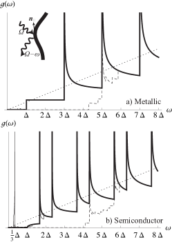
Several examples of the resulting Raman spectra of electronic excitations in metallic and semiconducting CNTs are plotted in Fig. 3(a,b). For each of the two nanotube types we show the spectra for undoped (solid line) and doped (dashed line) CNTs. For each value of the Raman shift spectral density plotted in Fig. 3 is composed from the contributions of several intersubband transitions with characteristic van Hove singularities. There is one exception from this rule: when the transitions turn on in undoped CNTs with , Raman intensity experiences a continuous increase from the threshold at , which is due to a peculiar -dependence of the transition amplitude in Eq. (10). Also, in metallic nanotubes, experiences a simple jump (Fig. 3(b)) when the lowest intersubband transitions turn on at , reflecting the linear dispersion of electrons in the subband with .
Doping of nanotubes allows for some intraband transitions with . Small doping with Fermi energy , allows for intraband transitions with the amplitude , including the most prominent line shown in Fig. 3(b), the only one which results in the intraband van Hove singularity at . For higher doping, , Raman spectrum is strongly suppressed at the energies due to the small Raman amplitudes of the intraband processes described by Eq. (10) and Pauli blocking of the interband processes with .

To summarize, we determined selection rules and calculated the spectral density of electronic excitations in the non-resonant Raman spectrum of a single-wall carbon nanotube of a given chirality. We found that the strongest Raman-active mode corresponds to the intersubband transition Note2 , and a characteristic CNT spectrum we obtained (see, e.g. in Fig. 3) features van Hove singularities corresponding to the electron excitations from/to the top/bottom of the corresponding nanotube subbands. These selection rules are specific for the non-resonant Raman scattering in large-radius nanotubes, where the e-h excitation energies are much less than the in/out photon energies.
The authors thank M. Potemski, T. Heinz, I. Aleiner, and J. Kürti for useful discussion and EPSRC and Royal Society for financial support.
References
- (1) R. Saito, G. Dresselhaus, and M. S. Dresselhaus, Physical properties of carbon nanotubes (Imperial College Press, 1998).
- (2) H. Kataura, Y. Kumazawa, Y. Maniwa, I. Umezu, S. Suzuki, Y. Ohtsuka, and Y. Achiba, Synthetic Met. 103, 2555 (1999).
- (3) Z. M. Li, Z. K. Tang, H. J. Liu, N. Wang, C. T. Chan, R. Saito, S. Okada, G. D. Li, J. S. Chen, N. Nagasawa, et al., Phys. Rev. Lett. 87, 127401 (2001).
- (4) S. M. Bachilo, M. S. Strano, C. Kittrell, R. H. Hauge, R. E. Smalley, and R. B. Weisman, Science 298, 2361 (2002).
- (5) A. Grüneis, R. Saito, G. G. Samsonidze, T. Kimura, M. A. Pimenta, A. Jorio, A. G. Souza Filho, G. Dresselhaus, and M. S. Dresselhaus, Phys. Rev. B 67, 165402 (2003).
- (6) F. Wang, G. Dukovic, L. E. Brus, and T. F. Heinz, Science 308, 838 (2005).
- (7) M. J. O’Connell, S. M. Bachilo, C. B. Huffman, V. C. Moore, M. S. Strano, E. H. Haroz, K. L. Rialon, P. J. Boul, W. H. Noon, C. Kittrell, et al., Science 297, 593 (2002).
- (8) A. Hartschuh, H. N. Pedrosa, L. Novotny, and T. D. Krauss, Science 301, 1354 (2003).
- (9) C. L. Kane and E. J. Mele, Phys. Rev. Lett. 90, 207401 (2003).
- (10) F. Wang, G. Dukovic, L. E. Brus, and T. F. Heinz, Phys. Rev. Lett. 92, 177401 (2004).
- (11) D. A. Tsyboulski, S. M. Bachilo, and R. B. Weisman, Nano Lett. 5, 975 (2005).
- (12) A. M. Rao, E. Richter, S. Bandow, B. Chase, P. C. Eklund, K. A. Williams, S. Fang, K. R. Subbaswamy, M. Menon, A. Thess, et al., Science 275(5297), 187 (1997).
- (13) R. Saito, T. Takeya, T. Kimura, G. Dresselhaus, and M. S. Dresselhaus, Phys. Rev. B 57, 4145 (1998).
- (14) A. Jorio, R. Saito, J. H. Hafner, C. M. Lieber, M. Hunter, T. McClure, G. Dresselhaus, and M. S. Dresselhaus, Phys. Rev. Lett. 86, 1118 (2001).
- (15) M. Dresselhaus, G. Dresselhaus, A. Jorio, A. S. Filho, and R. Saito, Carbon 40, 2043 (2002).
- (16) M. Dresselhaus, G. Dresselhaus, R. Saito, and A. Jorio, Phys. Rep. 409, 47 (2005).
- (17) W. H. Weber and R. Merlin, eds., Raman Scattering in Materials Science, Vol. 42 of Springer Series in Materials Science (Springer, 2000).
- (18) H. Farhat, S. Berciaud, M. Kalbac, R. Saito, T. F. Heinz, M. S. Dresselhaus, and J. Kong, Phys. Rev. Lett. 107, 157401 (Oct 2011).
- (19) O. Kashuba and V. I. Fal’ko, Phys. Rev. B 80(24), 241404 (2009).
- (20) M. Mucha-Kruczyński, O. Kashuba, and V. I. Fal’ko, Phys. Rev. B 82, 045405 (2010).
- (21) C. Faugeras, M. Amado, P. Kossacki, M. Orlita, M. Kühne, A. A. L. Nicolet, Y. I. Latyshev, and M. Potemski, Phys. Rev. Lett. 107(3), 036807 (2011).
- (22) P. Kossacki, C. Faugeras, M. Kühne, M. Orlita, A. Nicolet, J. Schneider, D. Basko, Y. Latyshev, and M. Potemski, arXiv:1110.4262 (2011).
- (23) P. M. Platzman, P. A. Wolff, and N. Tzoar, Phys. Rev. 174(2), 489 (1968).
- (24) Vectors and are lattice vectors of graphene, Å; for general chiral nanotube : for armchair and for zigzag .
- (25) H. Ajiki and T. Ando, Physica B: Cond. Mat. 201, 349 (1994).
- (26) One of those invokes intersubband transitions and , which are possible for “in” and “out” photons with the same polarizations. Similarly to graphene, the amplitude of the latter processes arises from an incomplete cancellation of two diagrams in Eq. (6) with commuting electron-photon interaction vertices (“in” and “out” photons with the same linear polarization) and after taking into account the deviations of electron Green’s functions in the intermediate states in Eq. (6) from the approximated . The amplitudes of such processes is less than in Eq. (7) by the factor . Such transitions may become stronger in small-radius nanotube, for which raman7el . Another weak transition is caused by the contact interaction between an electron and two photons simultaneously (the main inelastic scattering mechanism for non-relativistic electron plasma platzmanwolff ), which requires taking into account higher-order terms in the momentum expansion around the points in graphene Hamiltonian. The latter allows for weak transitions in all polarizations, transitions for crossed polarizations, and if both polarizations are perpendicular to the nanotube axis, with an amplitude , where is the width of the -band in graphene.