Rashba diamond in an Aharonov-Casher ring
Abstract
Spin interference due to Rashba spin-orbit interaction (SOI) in a ballistic two-dimensional electron gas (2DEG) ring conductor submitted to a bias voltage is investigated theoretically. We calculate the scattering matrices and differential conductance with lead-ring junction coupling as an adjustable parameter. Due to the interference of electronic waves traversing the ring, the differential conductance modulated by both bias voltage and SOI exhibits a diamond-shaped pattern, thus termed as Rashba diamond. This feature offers a supplementary degree of freedom to manipulate phase interference.
pacs:
73.23.-b, 03.65.Vf, 71.70.EjInterference phenomena, such as the celebrated Aharonov-Casher (AC) effect,ac-effect on a low-dimensional ring-shaped conductor patterned on a 2DEG with a Rashbarashba-soi SOI have attracted much attention.rashba-ring-theory ; aronov-lyandageller-1993 ; rashba-ring-exp Rashba SOI, due to structure inversion symmetry breaking, is dominating in quantum wells made of narrow gap semiconductorsnitta-1997-prl-and-engels-1997-prb and is among the most popular candidates to phase-coherent spintronic devices.datta-das ; nitta-1999-apl Recently, a large (at the order of ) while tunable Rashba parameter (controled by a gate voltage) has been achieved in InGaAs-based 2DEG systems. nitta-1997-prl-and-engels-1997-prb ; large-soi-parameter
We consider, in this letter, a one-dimensional (1D) ring conductor fabricated on a 2DEG with a Rashba SOI. In such a system, electrons experience an effective magnetic field that is perpendicular to the momentum while in the 2DEG plane. Electron waves that traverse the ring along clockwise and counterclockwise directions accumulate different phases that depend on and the incident energy, which is reflected in the interference patterns of the conductance. Most studies were focusing on the conductance as a function of gate electric fields (therefore ) and magnetic fields, see, Refs.rashba-ring-exp, and references therein. Nitta et al. proposed a gate-controlled spin-interference device on a ring conductor with a Rashba SOI, nitta-1999-apl while in this letter, we tune the interference patterns by applying a bias (therefore modifying the energy of incident electrons), thus offering a supplementary degree of freedom to control. We also address the impact of the lead-ring junction transparency on the interference 1984-buttiker-etal-pra which is usually ignored in the AC ring literature.
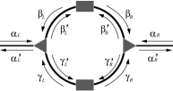
In Fig. 1, the desired ring conductor is connected to two leads. At low temperature, when the conducting channel length is comparable to the mean free path of electrons, a phase-coherent transport is justified.datta-book Meanwhile, the Dyakonov-Perel spin relaxation mechanismdyakonov-perel-pla is reduced in a two-dimensional strip.malshukov-chao-prb-and-kiselev-kim-prb ; nitta-jap-2009 Since the width of the ring branches is much shorter than the dimension along transport direction, the energy level splitting due to transverse confinement is much larger than the energy spacing along transport direction, which supports a single-channel transport.
A static electric field is applied perpendicularly to the 2DEG plane and the magnetic field is absent. The 1D single-particle Hamiltonian for electrons in the ring is2002-meijer-etal-prb (in cylindrical coordinates with an in-plane angle )
| (1) |
where is the effective mass of the electrons and is the radius of the ring. In cylindrical coordinates, the Pauli matrices are and . The eigenvalues of are given by
| (2) |
where the polarization index and the so-called AC phase ac-effect is , given . The corresponding normalized wave functions are , where the spinors are
| (7) |
given . When an electron of energy along the transport direction enters the ring (say, from the left lead), energy conservation requires
| (8) |
leading to and for each polarization (). The phase is the sum of the dynamical and the AC phases accumulated when traveling clockwisely (counterclockwisely).
Scattering matrix. The transport property of a coherent conductor is described by a scattering matrix.blanter-buttiker-pr We derive a total scattering matrix that converts the incoming amplitudes ( and , see Fig. 1) to the outgoing ones ( and ) for each eigenstate in Eq.(7). In the ballistic ring without spin-flip scatterings, we may treat and separately,aronov-lyandageller-1993 and the total conductance is the sum of the contributions from these two states.
On each branch, a scattering matrix is assigned to each spin polarization, i.e., on the upper branch and on the lower one (polarization index omitted for brevity). Since the spin-flip mechanism is suppressed, traversing a ring branch is equivalent to accumulating a phase shift. As an example, matching of the wave functions for spinor in the upper branch at two junctions gives the scattering matrix satisfying aronov-lyandageller-1993
| (15) |
and . Two components of the spinor differ by a phase factor that is unimportant, aronov-lyandageller-1993 thus neglected. Same consideration applies to spinor . At each junction (triangles as in Fig. 1) and for each polarization , three incoming waves (, and ) are scattered to the outgoing ones (, and ) by a symmetric scattering matrix 1984-buttiker-etal-pra
| (19) |
where the junction transparency : nazarov-book When , the ring is decoupled from the leads; when , an incoming wave is fully transmitted to two branches with equal probability. To keep the essential physics, we consider two identical junctions.
Transmission probability. Time-reversal symmetry leads to a symmetric that satisfies as required by current conservation. Total conductance , proportional to the total transmission probability , accounts contribution from two polarizations. When , the total transmission probability is
| (20) |
where is half of the AC phase difference between two polarizations. When (SOI vanishes), and can be understood as : In a fully transparent ring, the transmission probability of each polarization is unity. At a weak coupling , the total transmission probability is
| (21) |
where . It is interesting to notice that the case in Ref.molnar-etal-prb, corresponds to a transparency .
I-V curves. Applying a bias voltage () across the ring, the current (as a function of , temperature (), and ) is given by an energy integration
where and are the Fermi-Dirac distribution functions of the leads and is the Fermi energy.
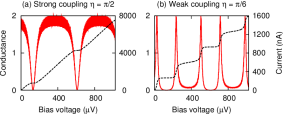
Figs. 2 show the step-like I-V curves upon scanning the bias voltage, which is similar to the Coulomb blockade in quantum dot systems, except that the plateaus in this AC ring is determined by the destructive interference of phases rather than the Coulomb repulsion. Fixing , decreasing makes the steps more developed and the conductance peaks sharper. The width of the conductance peak, as broadened by the lead-ring coupling,aronov-lyandageller-1993 ; 1984-buttiker-etal-pra reflects the lifetime of an electronic state inside the ring: The narrower is the peak the longer is the lifetime. 1984-buttiker-etal-pra When is small, the total transmission probability
| (22) |
where as introduced in Ref. 1984-buttiker-etal-pra, . The singularities of the transmission probability in Eq.(22) are determined by the solutions of which is exactly the eigenvalue equation Eq. (8).
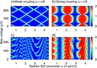
Rashba diamond. Fig. 3 shows the differential conductance () modulated by both (horizontal axis) and (vertical axis). The presence of Rashba diamonds in panels (a) and (b), reminds us again the Coulomb diamonds in a system consisting of, e.g. quantum dots. nazarov-book For a given and , the bias fully controles the conductance, thus leading to a new degree of freedom to manipulate the interference-induced current modulation. The panels (a) and (b) in Fig. 3 are for a quantum well based on InGaAs/InAlAs.nitta-jap-2009 In the weak coupling regime, the Rashba diamonds are more developed than in the strong coupling limit.
In a realistic 2DEG, the gate voltage modulates both and carrier density (therefore the Fermi level). ando-rmp We take the experimental data on an InGaAs/InAlAs based 2DEG from Ref.nitta-jap-2009, (the 10nm quantum wells in Fig.3 of Ref.nitta-jap-2009, ), from which a linear relationship between and Fermi level is established to calculate the differential conductance. In panels (c) and (d) of Fig.3, distorted Rashba diamonds appear as the Fermi level is adjusted simultaneously when changing . The periodicity due topological phase interference (through ) survives, which is particularly clear in the strong coupling limit.
To circumvent the experimental difficulty of applying a well defined voltage bias, leturcq-prl energy barriers formed using gate electrodes at the ring-lead junctions are suggested. The advantage of gate electrode is the flexibility to tune the height of the barrier thus the junction transparencies. Non-magnetic tunnel barriers are good candidates as well since we do not expect significant spin-flip scattering at the junctions. Another experimentally relevant geometry consists a ring conductors with two branches interrupted by tunnel barriers or gate electrodes, as in the electric Aharonov-Bohm experiment.vanderwiel-prb
In conclusion, for an AC ring with a Rashba SOI, we have investigated the interference patterns due to topological phases. The scattering matrices, as parametrized by junction transparency, were obtained analytically. We have demonstrated the possibility to control the differential conductance by both a bias voltage and an electric field. A diamond-shaped pattern of the conductance is well developed in the weak coupling regime, which provides a supplementary degree of freedom to manipulate spins in the Rashba SOI based spintronic devices.
References
- (1) Y. Aharonov and A. Casher, Phys. Rev. Lett. 53, 319 (1984).
- (2) Yu. A. Bychkov and E. I. Rashba, J. Phys. C: Solid State Phys. 17, 6039 (1984).
- (3) Y. Meir, Y. Gefen, and O. Entin-Wohlman, Phys. Rev. Lett. 63, 798 (1989); A. Stern, ibid. 68, 1022 (1992); Y. Lyanda-Geller, ibid. 71, 657 (1993); D. Frustaglia and K. Richter, Phys. Rev. B 69, 235310 (2004); S. Q. Shen, Z. J. Li and Z. Ma, Appl. Phys. Lett. 84, 996 (2004). S. Souma and B. K. Nikolić, Phys. Rev. Lett. 94, 106602 (2005); M. F. Borunda, X. Liu, A. A. Kovalev, X. -J. Liu, T. Jungwirth, and J. Sinova, Phys. Rev. B 78, 245315 (2008).
- (4) A. G. Aronov and Y. B. Lyanda-Geller, Phys. Rev. Lett. 70, 343 (1993).
- (5) A. F. Morpurgo, J. P. Heida, T. M. Klapwijk, and B. J. van Wees, Phys. Rev. Lett. 80, 1050 (1998); J. -B. Yau, E. P. De Poortere, and M. Shayegan, ibid. 88, 146801 (2002). M. König, A. Tschetschetkin, E. M. Hankiewicz, J. Sinova, V. Hock, V. Daumer, M. Schafer, C. R. Becker, ̵̈H. Buhmann, and L. W. Molenkamp, ibid. 96, 076804 (2006).
- (6) J. Nitta, T. Akazaki, H. Takayanagi, and T. Enoki, Phys. Rev. Lett. 78, 1335 (1997); G. Engels, J. Lange, Th. Schäper, and H. Lüth, Phys. Rev. B 55, 1958 (1997); T. Koga, J. Nitta, T. Akazaki, and H. Takayanagi, Phys. Rev. Lett. 89, 046801 (2002).
- (7) S. Datta and B. Das, Appl. Phys. Lett. 56, 665 (1990).
- (8) J. Nitta, F. E. Meijer and H. Takayanagi, Appl. Phys. Lett. 75, 695 (1999).
- (9) D. Grundler, Phys. Rev. Lett. 84, 6074 (2000); Y. Sato, T. Kita, S. Gozu, and S. Yamada, J. Appl. Phys. 89, 8017 (2001).
- (10) M. Büttiker, Y. Imry and M. Ya. Azbel, Phys. Rev. A 30, 1982 (1984).
- (11) S. Datta, Electron Transport in Mesoscopic Systems (Cambridge University Press, Cambridge, 1995).
- (12) M. I. Dyakonov and V. I. Perel, Phys. Lett. A 35, 459 (1971).
- (13) A. G. Mal’shukov and K. A. Chao, Phys. Rev. B 61, 2413 (2000); A. A. Kiselev and K. W. Kim, ibid. 61, 13115 (2000); S. Kettemann, Phys. Rev. Lett. 98, 176808 (2007).
- (14) J. Nitta, T. Bergsten, Y. Kunihashi, and M. Kohda, J. Appl. Phys. 105, 122402 (2009).
- (15) F. E. Meijer, A. F. Morpurgo and T. M. Klapwijk, Phys. Rev. B 66, 033107 (2002).
- (16) Y. Blanter and M. Büttiker, Phys. Rep. 336, 1 (2000).
- (17) B. Molnár, F. M. Peeters, and P. Vasilopoulos, Phys. Rev. B 69, 155335 (2004).
- (18) T. Ando, A. B. Fowler and F. Stern, Rev. Mod. Phys. 54, 437 (1982).
- (19) Yu. V. Nazarov and Ya. M. Blanter Quantum Transport (Cambridge University Press, Cambridge, 2009).
- (20) R. Leturcq, D. Sanchez, G. Gotz, T. Ihn, K. Ensslin, D. C. Driscoll, and A. C. Gossard, Phys. Rev. Lett. 96, 126801 (2006).
- (21) W. G. van der Wiel, Yu. V. Nazarov, S. De Fanceschi, T. Fujisawa, J. M. Elzerman, E. W. G. M. Huizeling, S. Tarucha, and L. P. Kouwenhoven, Phys. Rev. B 67, 033307 (2003).