Native defects in hybrid C/BN nanostructures
Abstract
First-principles calculations of substitutional defects and vacancies are performed for zigzag-edged hybrid C/BN nanosheets and nanotubes which recently have been proposed to exhibit half-metallic properties. The formation energies show that defects form preferentially at the interfaces between graphene and BN domains rather than in the middle of these domains, and that substitutional defects dominate over vacancies. Chemical control can be used to favor localization of defects at C-B interfaces (nitrogen-rich environment) or C-N interfaces (nitrogen-poor environment). Although large defect concentrations have been considered here (106 cm-1), half-metallic properties can subsist when defects are localized at the C-B interface and for negatively charged defects localized at the C-N interface, hence the promising magnetic properties theoretically predicted for these zigzag-edged nanointerfaces might not be destroyed by point defects if these are conveniently engineered during synthesis.
pacs:
73.20.-r, 73.20.Hb, 73.22.PrI Introduction
Hybrid C and BN nanostructures have been studied since the first attempts to dope carbon nanotubes with boron or nitrogen. Stephan et al. (1994) Nanotubes (NT) with C, B, and N were theoretically predictedMiyamoto et al. (1994) and experimentally synthesized in the mid 90s, Stephan et al. (1994); Chopra et al. (1995); Redlich et al. (1996); Suenaga et al. (1997) but the recent advent of graphene has revitalized the field. Hybrid C and BN nanosheets are becoming accesibleHan et al. (2008); Ci et al. (2010) offering a new route to enhance graphene’s promise, enabling for fine-tuning the electronic and optical properties (for example modulation of the electronic bandgap, chemical reactivity, etc).
Following the advances in experimental growth of hybrid C-BN nanostructures, Ci et al. (2010); Enouz et al. (2007); Wei et al. (2011) the stability of domain-separated C and BN nanosheets and nanotubes has been studied by first principles simulations in the last couple of years. Ding et al. (2009); Du et al. (2009); Z.-Y. Zhang and Guo (2009); Ivanovskaya et al. (2009); An and Turner (2010) There is general agreement that segregation is energetically advantageous, because B-N and C-C bonds are more stable than C-N and C-B and the former are favored by the formation of C and BN domains. Furthermore, according to molecular dynamics simulations, hybrid C-BN armchair nanotubes can be spontaneously formed via the connection of zigzag-edged BN and graphene nanoribbons (BNNR and GNR) at room temperature, Du et al. (2009) and their stability can be competitive with that of the corresponding pristine BNNTs and CNTs. An and Turner (2010) These zigzag-edged heterostructures are particularly appealing for spintronic applications, as the polarity of the BNNR gives an interfacial dipole, hence an effective electric field acting on the graphene ribbon. Pruneda (2010) It has been predicted that half-metallicity can be induced in zigzag-GNRs by application of a sufficiently large in-plane electric field perpendicular to the edges of the ribbon. Son et al. (2006)
Magnetism in zigzag-edged graphene-based nanostructures is related to the presence of electronic states that are mainly localized at the edges. Fujita et al. (1996) These states seem to be ubiquitous in hexagonal structures with zigzag bordersOkada et al. (2000), and are not present in armchair edges. Roughness and defects have been shown to strongly affect the electronic properties of zigzag-GNR, inducing a continous decrease of the magnetic moments with increasing concentration of defects until the system becomes nonmagnetic for concentrations of one defect per 10Å, which might be a typical concentration for real samples. Huang et al. (2008) Nevertheless half-metallicity induced by external electric fields seems to survive at similar defect concentrations with the same critical field strength. Son et al. (2006) At zigzag interfaces between C and BN domains, however, defects can change the electronic screening of the edge polarity hence affecting the effective electric potential on graphene’s ribbon and destroying its intrinsic half-metallicity. It is then important to address the role played by point defects at the boundary between graphene and BN domains. In this work, first principles simulations are performed to determine the formation energies and electronic properties of intrinsic point defects (vacancies and substitutional defects) at zigzag interfaces between C and BN nanodomains that could exhibit magnetism. It is shown that these defects are energetically favored when localized close to domain interfaces, and their electronic properties are determined by the presence of a defect-induced electronic state localized at the C-N interface which could be occupied or empty depending on the donor/acceptor nature of the defect.
The paper is organized as follows. After describing the technicalities in section II, we present and discuss the findings in III. Results of the energetics of neutral defects at the interfaces are examined and compared to similar defects placed at a graphene-like or BN-like monodomain. Magnetism at the interfaces and other electronic properties are then analysed, and the effect of defect concentration and charge state discussed. Finally, section IV summarizes the conclusions.
II Methodology
Ab initio pseudopotential density functional calculations are performed for both planar (2D) superlatticesPruneda (2010), and (n,n) armchair nanotubes (5n14) with zigzag edged C-BN domains along the tube axis following the geometries discussed in the literature. Du et al. (2009); Z.-Y. Zhang and Guo (2009); An and Turner (2010); Huang et al. (2010) Troullier-Martin type pseudopotentialsTroullier and Martins (1991) and numerical atomic orbitals with double- plus polarization are used to describe the electronic valence states within the spin-polarized generalized-gradient approximationPerdew et al. (1996) as implemented in the SIESTA code. Soler et al. (2002) The atomic positions are determined with a structural relaxation until the forces are smaller than 0.02eV/Å. An accurate description of the boundary electronic states requires a smooth sampling of the reciprocal space, and typically Monkhorst-Pack grids of at least 11100 is used to sample the Brillouin zone.
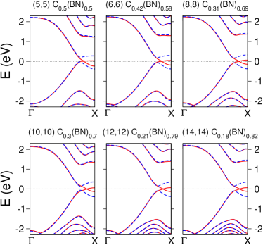
It has been claimed that half-metallicity in C-BN nanotubes can be achieved within a certain ratio of carbon content (30%-50%) and is not dependent on the diameter of the tube. Huang et al. (2010) This allegation can be misleading. Although half-metallic ground states can be obtained for different chiralities (see Fig.1), this only happens for C-concentrations under a critical value, that does depend on the tube diameter. Analogously to the case of planar C-BN heterostructures, the critical parameter is the relative width of the C- and BN-strips. Pruneda (2010) To address the stability of magnetism to the presence of defects, systems that hold half-metallic properties in their pristine (defect-free) structure, are considered. In particular, throughout this work we take: (i) nanotube with chirality (5,5) and 50% C concentration (corresponding to 5 C and 5 BN zigzag chains), and (ii) planar (5,7) C-BN superlattice (composed by 5 C and 7 BN zigzag chains). Native point defects are introduced near the edges of the C and BN domains in a supercell geometry, with at least 30 Å empty space in-between periodic images. Different concentrations can be modeled by changing the size of the supercell along the periodic axis. If not otherwise stated, supercells made out of 8 repetitions of the unit cell along the tube axis are considered (a total of 160 atoms).
The formation energy of a defect in charge state is defined in terms of the chemical potentials of the species involved in the defect, and the Fermi level, , measured relative to the top of the valence band :
where is the energy of the defective supercell containing atoms of species (C, B, and N) with chemical potential , at (entropic contributions are neglected). These chemical potentials are specified by a reference system that acts as the reservoir of atoms. Typically reference values used in the literature are taken from graphene, molecular nitrogen, and bulk boron. These, however, will only give formation energies under limits of high concentrations of C, N, or B. Formally, one can use the formation energies of these reference systems as thermodyncamic limits to the chemical potentials, which must satisfy the following conditions:
-
1.
stability of the C-BN complex:
(1) -
2.
The values that cause precipitation into its constituents,
-
3.
The values that cause formation of each domain
where denotes the generalized formation free energy of the corresponding system relative to pure C or BN nanotube. Relation (1) can be used to write one of the atomic chemical potentials in terms of the other two. Considering that C-doping in BNNT had proved elusiveC-d , whereas BNNT can be synthesized by substitutional reaction from CNTHan et al. (1998), in the following the chemical potential of C will be set to the value that corresponds to clean CNT, meaning that the defect formation energies will be given in the C-rich limit, and only will be used as free parameter.
III Results and Discussion
Substitutional carbons on the boron and nitrogen sublattices (C and C), boron or nitrogen atoms in carbon sites (B and N) and vacancies of each species (V, V and V) were considered, as shown in figure 2. Ghost orbitals are used to improve the localized atomic orbital description at the vacancy sites. Labels and will be used to denote the edge at which the defect is placed, where designates the interface with bonds, whereas is the edge with bonds. Accordingly defects are classified into set N (C, B, V, V, or V), and set B (C, N, V, V, or V).
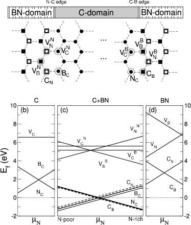
The formation energies for the interfacial (neutral) defects in (5,5) C-BN nanotube are shown in Fig.2 and compared to the energetics of the same defects in a pristine pure-CNT and pure-BNNT of the same chirality. The energies of pure C and BN nanotubes are in agreement with values published in the literatureA. V. Krasheninnikov et al. (2006); Koretsune and Saito (2008); Piquini et al. (2005), considering that the formation energy depends on the chirality, and increases with tube’s diameterA. V. Krasheninnikov et al. (2006); Gou et al. (2007). The cost of removing atoms (vacancy formation) is generally larger than the energy of atom substitution (disorder), which is indicative of the high stability of the honeycomb structure. First principles calculations have shown that vacancy formation is energetically more favorable near the edge of zigzag BNNRs than in the center of the ribbonTang and Cao (2010). A similar effect is observed now, with defects at the edge being at least 1 eV less energetic. Interestingly, recent experiments have shown that carbon substitution (doping) in BN nanostructures is favored at the edges. Wei et al. (2011)
Note that C and B (defects of set N) are energetically favorable in a nitrogen-poor environment (B-rich), and the same is true for N and C (set B) in N-rich situation, so that the localization of defects at each edge of the heterojunction could be chemically controled. Furthermore, when neutral C and B defects are formed, one hole is added to the system, so that these defects can act as electron traps. On the other hand, N and C add one extra electron to the system and could possibly become positively charged under appropriate conditions (low electron chemical potential ). In pure BN nanosheets and nanotubes, V is also an acceptor that can trap charges to form V, whereas V has two one-electron states in the gap, one occupied and the other empty, enabling the formation of both V or V, depending on the value of .
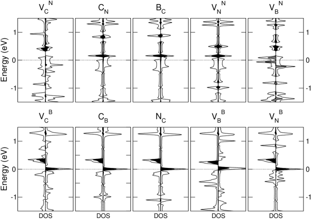
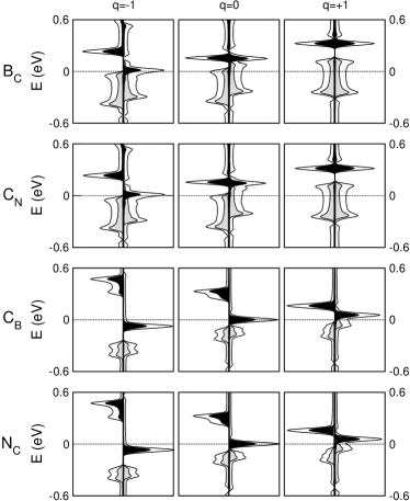
Figure 3 shows the electronic Density of States (DOS) for set N (top) and set B defects. Notice that, even for the high defect concentration considered in these simulations (5cm-1), the later remain half-metallic, with a sharp peak in the DOS at the Fermi level. This peak corresponds to a defect-induced electronic state that is localized at the N-edge rather than at the defect itself (placed at the B-edge). Hence, electrons coming from these donor defects are transferred through the C-domain to the region with lower electronic potential, as described in reference Pruneda, 2010. This can be seen from the DOS projected on the carbon orbitals localized at the C-N interface (shaded regions in the figure). This localized band has some dispersion along the edge axis (there is slightly more contribution to the pDOS from C atoms directly opposite to the defect site), and a larger unit cell would be needed to address its localization length. The exchange splitting for this band is 0.3 eV for all the set B defects, and the calculations give a total magnetic moment of 1 for C, N and V, 2 for V, and 3 for V.
On the other hand, the missing electron (extra hole) for set N defects has a dramatic effect the corresponding DOS, that does not show half-metallic properties. There is a similar defect-induced electronic state localized at the C-N interface for C, B and V, but now it is unoccupied (0.1 eV above the Fermi level) and not spin-polarized (C and B have a total magnetic moment of 0.5 ). V and V are slightly different, with an empty C-N interfacial state at 0.4 eV above the Fermi level, and a rather localized electronic state on the atoms surrounding the vacancy site (shaded light regions in the figure) which is spin-polarized (total magnetization of 1.8 and 1, respectively. The lowering of the Fermi level means a partial depopulation of the state, Pruneda (2010) and a weakening of the magnetic instability induced by electron-electron interactionsFujita et al. (1996). The reduction of the electronic occupation of the state lowers the electronic potential at the B-edge, and significant decrease of the induced electric field in the graphene ribbon, so that half-metallicity cannot survive. Pruneda (2010)
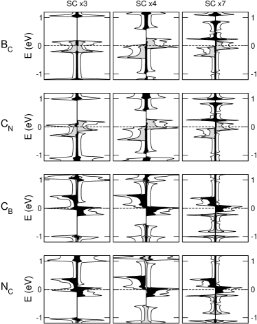
Let’s focus in the following on those defects that have the lower formation energies, i.e. substitutionals. The effect of increasing the defect concentration even further is shown in figure 4, where the DOS of different supercells of planar bidimensional superlattices are shown. Small differences arise between this planar geometry and the previous tubular case, mainly because of the different C/BN ratio, but the general results are equivalent. For p-type set N defects (B and C) the reduced number of electrons shifts the Fermi level towards lower values as we move towards higher defect concentrations (smaller supercells, from right to left), depopulating the initially fully occupied majority spin band, localized at the C-B interface (light shaded region), until the full spin polarization at the Fermi level is destroyed. On the other hand, for n-type set B defects (N and C), the extra electrons added to the system shifts the Fermi level to higher values as we move towards higher concentrations, increasing the occupation of the C-N electronic states, and eventually destroying half-metallicity. Notice again that defects localized at the C-B interface add extra electrons that are transferred to the C-N interface, while defects localized at the C-N interface, which are electron deficient tend to remove charge from the C-B interface.
For the limit of low concentration of defects, the semimetallic graphene domain could be considered as the electron reservoir so that is fixed by the position of GNR’s Fermi level, and hence only neutral defect calculations were considered up to now. However the donor/acceptor character of the defects has become relevant when discussing their electronic properties, revealing the need to address charged defects. When addressing charge states for defects in semiconductors and insulatores, the value of in equation (II) ranges between zero (the top of the valence band) and the energy band gap, and a careful alignment of the reference energy has to be considered to compare energetics of neutral and charged defects. Here, however, the system is semimetallic regardless of the charge state, so that the position of the Fermi level can be used to align the energetics, and can be used to compare formation energies.
As shown in figure 5, when an extra electron is added to the system (), it localizes at the N-edge state (dark peaks) close to the Fermi level, recovering half-metallicity for the set N defects (the states become fully occupied for set B defects which remain half-metallic). The formation energies for these charged defects are reduced by 2.3 eV (at eV). There is a decrease in the system’s total magnetization for set N (0.1 ) and an increase to 2 for set B. On the other hand, removal of an electron (giving defects with charge state ) has negative effects on the electronic properties of substitutionals: the lowering of the Fermi level depopulates the N-edge state for set B defects (although the total DOS remains half-metallic), and destroys magnetization for all defects (set N remains metallic). In this case, the formation energies are increased by 3.6 eV, clearly destabilizing these positively charged defects.
Following the above results, a N-rich environment together with a high (providing electrons to the system) would increase the possibilities for subsistence of half-metallicity in these hybrid C-BN structures. B-edge localized defects are favored by an N-rich atmosphere and even at large defect concentrations (106 cm-1) conducting electrons remain fully spin-polarized. On the other hand, under these chemical conditions, there would be a lower concentration of defects localized at the N-edge (higher formation energies), which although hinder half-metallicity when neutral, they do not in their negative charge state. It is interesting that similar conditions have been suggested to be best for manufacturing hybrid compounds through electron-beam-induced doping of BN nanostructures with C. Berseneva et al. (2011)
IV Conclusions
First principles DFT calculations have shown that intrinsic defects in hybrid C-BN nanostructures are more stable at the boundaries between C and BN domains. Both bidimensional superlattices of alternating graphene and BN nanoribbons, and armchair nanotubes with axial domains of C and BN that have zigzag edges have been analysed, giving similar results. In these systems, the electronic bandstructure close to the Fermi level is determined by characteristic zigzag-edge states localized at the boundary of the hexagonal lattice, as already discussed in the literature.
The stability of the honeycomb structure results in a higher formation energy for vacancies (V, V, or V) than for substitutionals. While a nitrogen-poor environment favors the formation of defects at C-N interfaces (mainly C and B), nitrogen-rich atmospheres favors defects localized at the C-B boundary (C and N), which could be classified as electron acceptors and donors respectively. Extra electrons provided by the latter are transferred to a defect-induced partially occupied electronic state localized at the opposite edge (C-N) and the system would remain half-metallic, even for the large defect concentrations considered here. If extra electrons are added to the system, they are transferred to this electronic state and the defect would be further stabilized (in their negatively charged state), whereas electron-deficiency drains the electronic level and increases the defect formation energy. On the other hand, substitutional defects localized at the C-N interface, add one hole to the system hence lowering the Fermi level and weakening the magnetic instability (through depopulation of the orbital) resulting in the cancelation of half-metallicity. The defect-induced electronic state localized at the C-N interface is still there, but unoccupied. Extra electrons added to the system would populate this level, recovering half-metallicity and lowering the defect formation by a couple of eV.
Finally, the analysis of the magnetic properties reveals that half-metallicity (i) could survive defect concentrations at the interfacial line of up to 107 cm-1, and (ii) could be tuned through appropriate electronic doping that avoids an excesive charge depletion from the C-B interface for high concentrations of p-type substitutionals or excesive charge increase at the C-N interface for n-type substitutionals. Experimental investigation of magnetism in these hybrid nanostructures is encouraged.
Acknowledgements.
The author acknowledges financial support by the Spanish MCINN (FIS2009-12721-C04-01 and CSD2007-00041).References
- Stephan et al. (1994) O. Stephan, P. M. Ajayan, C. Colliex, P. Redlich, J. M. Lambert, P. M. Bernier, and P. Lefin, Science 266, 1683 (1994).
- Miyamoto et al. (1994) Y. Miyamoto, A. Rubio, M. L. Cohen, and S. G. Louie, Phys. Rev. B 50, 4976 (1994).
- Chopra et al. (1995) N. G. Chopra, R. J. Luyken, K. Cherrey, V. H. Crespi, M. L. Cohen, S. G. Louie, and A. Zettl, Science 269, 966 (1995).
- Redlich et al. (1996) P. Redlich, J. Loeffler, P. M. Ajayan, J. Bill, F. Aldinger, and M. Ruhle, Chem. Phys. Lett 260, 465 (1996).
- Suenaga et al. (1997) K. Suenaga, C. Colliex, N. Demoncy, A. Loiseau, H. Pascard, and F. Willaime, Science 278, 653 (1997).
- Han et al. (2008) W. Q. Han, L. Wu, Y. Zhu, K. Watanabe, and T. Taniguchi, Appl. Phys. Lett. 93, 223103 (2008).
- Ci et al. (2010) L. Ci, L. Song, C. Jin, D. Jariwala, D. Wu, Y. Li, A. Srivastava, Z. F. Wang, K. Storr, L. Balicas, et al., Nat. Mater. 9, 430 (2010).
- Enouz et al. (2007) S. Enouz, O. Stéphan, J.-L. Colliex, and A. Loiseau, Nano Letters 7, 1856 (2007).
- Wei et al. (2011) X. Wei, M. S. Wang, Y. Band, and D. Golberg, ACS Nano 5, 2916 (2011).
- Ding et al. (2009) Y. Ding, Y. Wang, and J. Ni, Appl. Phys. Lett. 95, 123105 (2009).
- Du et al. (2009) A. Du, Y. Chen, Z. Zhu, G. Lu, and S. C. Smith, J. Am. Chem. Soc. 131, 1682 (2009).
- Z.-Y. Zhang and Guo (2009) Z. Z. Z.-Y. Zhang and W. Guo, J. Phys. Chem. C 113, 13108 (2009).
- Ivanovskaya et al. (2009) V. V. Ivanovskaya, A. Zobelli, O. Stéphan, P. R. Briddon, and C. Colliex, J. Phys. Chem C 113, 16603 (2009).
- An and Turner (2010) W. An and C. H. Turner, J. Phys. Chem. Lett. 1, 2269 (2010).
- Pruneda (2010) J. M. Pruneda, Phys. Rev. B 81, 161409(R) (2010).
- Son et al. (2006) Y.-W. Son, M. L. Cohen, and S. G. Louie, Nature 444, 347 (2006).
- Fujita et al. (1996) M. Fujita, K. Wakabayashi, K. Nakada, and K. J. Kusakabe, J. Phys. Soc. Jpn. 65, 1920 (1996).
- Okada et al. (2000) S. Okada, M. Igami, K. Nakada, and A. Oshiyama, Phys. Rev. B 62, 9896 (2000).
- Huang et al. (2008) B. Huang, F. Liu, J. Wu, B. L. Gu, and W. Duan, Phys. Rev. B 77, 153411 (2008).
- Huang et al. (2010) B. Huang, C. Si, H. Lee, L. Zhao, J. Wu, B.-L. Gu, and W. Duan, Appl. Phys. Lett. 97, 043115 (2010).
- Troullier and Martins (1991) N. Troullier and J. L. Martins, Phys. Rev. B 43, 1993 (1991).
- Perdew et al. (1996) J. P. Perdew, K. Burke, and M. Ernzerhof, Phys. Rev. Lett. 77, 3865 (1996).
- Soler et al. (2002) J. M. Soler, E. Artacho, J. D. Gale, A. García, J. Junquera, P. Ordejón, and D. Sánchez-Portal, J. Phys.: Condens. Matter 14, 2745 (2002).
- (24) C-doping can be achieved in BN nanosheets and nanotubes through in situ electron-beam irradiation as a post-synthesis process Wei et al. (2011).
- Han et al. (1998) W. Q. Han, Y. Bando, K. Kurashima, and T. Sato, Appl. Phys. Lett. 73, 3085 (1998).
- A. V. Krasheninnikov et al. (2006) P. P. L. A. V. Krasheninnikov, A. S. Foster, and R. M. Nieminen, Chem. Phys. Lett. 418, 132 (2006).
- Koretsune and Saito (2008) T. Koretsune and S. Saito, Phys. Rev. B 77, 165417 (2008).
- Piquini et al. (2005) P. Piquini, R. J. Baierle, T. M. Schmidt, and A. Fazzio, Nanotechnology 16, 827 (2005).
- Gou et al. (2007) G. Y. Gou, B. C. Pan, and L. Shi, Phys. Rev. B 76, 155414 (2007).
- Tang and Cao (2010) S. Tang and Z. Cao, Comp. Mater. Sci. 48, 648 (2010).
- Berseneva et al. (2011) N. Berseneva, A. V. Krasheninnikov, and R. M. Nieminen, Phys. Rev. Lett. 107, 035501 (2011).