Tunable capacitive inter-dot coupling in a bilayer graphene double quantum dot
Abstract
We report on a double quantum dot which is formed in a width-modulated etched bilayer graphene nanoribbon. A number of lateral graphene gates enable us to tune the quantum dot energy levels and the tunneling barriers of the device over a wide energy range. Charge stability diagrams and in particular individual triple point pairs allow to study the tunable capacitive inter-dot coupling energy as well as the spectrum of the electronic excited states on a number of individual triple points. We extract a mutual capacitive inter-dot coupling in the range of 2 - 6 meV and an inter-dot tunnel coupling on the order of 1.5 eV.
I Introduction
Graphene is a promising material for future quantum devices and quantum information technology trau07 . In particular, graphene quantum dot devices are interesting candidates for
spin qubits with long coherence times. The weak spin-orbit coupling min06 ; hue06 and weak hyperfine interaction is
expected to be of advantage compared to state-of-the-art GaAs-devices. However, the gapless band structure of graphene makes it hard to electrostatically confine charge carriers. This can be overcome by nanostructuring graphene, where it has been shown that an etching-based ”paper cutting” technique leads to graphene nanodevices where transport is dominated by a disorder-induced energy gap. Consequently, graphene nanoribbons chen07 ; han07 ; mol09 ; stam09 ; tod09 ; liu09 ; gal10 ; han10 ; ter11 , single-electron transistors (SETs) sta08 ; stam08nano ; ihn10 , graphene quantum dots (QD) gue08 ; pon08 ; sch09 even with charge detectors gue08 ; gue11 ; wan10a and graphene double quantum dots mol09a ; mol10a ; liu10 ; wan10 ; Volk2011 have been demonstrated successfully.
These devices allowed the experimental observation of excited states sch08 ; mol10a , spin states gue10 and the very few carrier regime gue09 .
Almost all of these studies were based on single-layer graphene and showed device limitations related to the presence of edge roughness, disorder and unintended vibrational degrees of freedom mas10 . Bilayer graphene is an interesting candidate to overcome some of these shortcomings.
In particular, bilayer graphene allows to open a band gap by an out-of-plane electric field oos08 ; zha09 , which may enable a
soft confinement potential and may reduce the influence of localized edge states. Furthermore, it is expected that ripples and substrate-induced disorder are reduced, which may also increase the mechanical stability suppressing unwanted vibrational modes.
Here we present a bilayer graphene double quantum dot with a number of lateral gates. The gates allow to tune transport over a wide energy range
and they enable to operate the device in different configurations. We focus on the double quantum dot (DQD) configuration and show characteristic honeycomb-like charge stability diagrams. More specifically, we discuss the electrostatic tunability of the mutual capacitive inter-dot coupling energy. Finally, we also extract an inter-dot tunnel coupling energy.
II Device Fabrication
The device is fabricated by mechanical exfoliation of natural graphite by adhesive tapes nov04 ; nov05 . The substrate material consists of highly doped silicon (Si++) bulk material covered with around 300 nm of silicon oxide (SiO2) in order to identify bilayer graphene flakes due to absorption and interference. Before deposition, reference alignment markers are patterned on the substrate to relocate the flakes for further processing and characterization. In particular Raman spectroscopy measurements are used to identify bilayer graphene flakes fer06 ; graf07 .
The graphene flakes have to be structured to submicron
dimensions in order to fulfill the device design requirements.
We use a technique based
on resist spin coating, electron beam lithography (EBL),
development and subsequent etching of the unprotected
graphene. We use an EBL resist
[polymethylmethacrylate (PMMA)] with a thickness of
80 nm and short etching time to define the nanoscale structures.
We follow earlier work sta08 , where it has been shown that
short (5 s) mainly physical reactive ion etching (RIE)
based on argon and oxygen (80:20) provides good results
without influencing the overall quality of the graphene flake mol07 . After etching and removing the residual EBL resist, the
graphene nanostructures are contacted by an additional
EBL step, followed by metalization and lift-off. Here we
evaporated 5 nm chrome (Cr) and 50 nm gold (Au) for
contacting the bilayer graphene double quantum dot device.
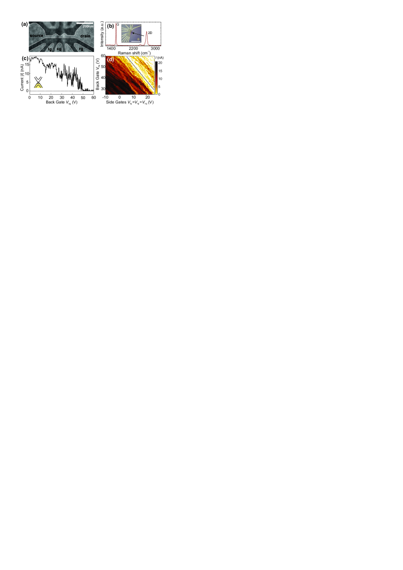
A scanning force microscope image of the investigated device is shown in Figure 1(a), where the graphene structures (bright areas) resting on SiO2 (dark areas) are highlighted by the white dashed lines. The bilayer double quantum dot consists of three 30 nm wide and 50 to 100 nm long constrictions, two are separating the source and drain leads from the double quantum dot and one is separating the left (LQD) from the right (RQD) quantum dot. Both bilayer graphene quantum dots have a diameter of approximately 50 nm. In this study we use the left (lg) and the right (rg) gate to change the number of carriers in the left and the right QD, while the central gate (cg) is used to tune the inter-dot coupling. Additionally, the back gate (bg) is used to adjust the overall Fermi level. The Raman spectrum shown in Figure 1(b) shows that the investigated device is indeed based on a bilayer graphene flake (see also Fig. 1(b) in Ref. Volk2011 ). The FWHM of the 2D-peak is 57.9 cm-1 with a 18.8 cm-1 spacing of the two inner Lorentzian peaks which in combination with the shoulder on the left side (see 2D peak in Figure 1(b)) provides a good finger print for the bilayer nature fer06 ; graf07 . The inset in Figure 1(b) shows an optical image of the contacted device (see arrow).
III Measurements
The measurements have been performed in a dilution refrigerator at a base temperature of 10 mK. We have measured the two-terminal conductance through the bilayer graphene double quantum dot by applying a symmetric dc bias voltage while measuring the current through the device with a resolution better than 50 fA.
III.1 Device Characterization
To characterize the double quantum dot device on a large energy scale the back gate voltage is tuned over a range of 60 V. Figure 1(c) shows the source-drain current as a function of the back gate voltage. We observe a so-called transport gap stam09 above V ( mV) and hole dominated transport for lower back gate voltages (see inset in Fig. 1(c)). The large-scale current fluctuations in the transport gap region of the DQD device are due to local resonances in the bilayer graphene constrictions acting as tunneling barriers. In Figure 1(d) we show a measurement of the current as a function of the back gate voltage and the left, right and central gate voltages () at constant bias ( mV).
One characteristic slope is observed, which separates the area of suppressed current (upper right corner) from the area of elevated hole transport (lower left corner). The three tunneling barriers can be tuned almost equally by either the back gate or the sum of the left, right and central gates ( = 1.5), which is in a good agreement with the device design and with earlier studies gue09 .
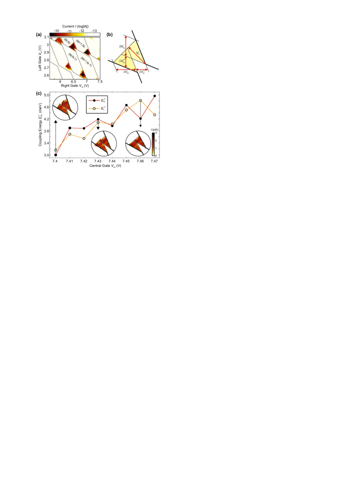
By fixing the back gate and the central gate voltage we can record charge stability diagrams by varying the left and right gate voltages independently. In Figure 2(a) we show a finite bias ( 8 mV) measurement, where the honeycomb pattern is observed, which is characteristic for the charge stability diagram of a DQD Wiel2002 . It is crucial that electrical transport through the DQD is only possible in the case where the energy levels in both quantum dots are aligned within the source-drain bias window. From this measurement we can extract the lever arms and the single quantum dot addition energies, such as 23 meV and 13 meV for the left and right quantum dot, respectively.
III.2 Capacitive Inter-dot Coupling
In this section we discuss the effect of the central gate voltage on the capacitive coupling between the left and the right quantum dot (i.e. the capacitive inter-dot coupling). In Figure 2(b) we show a schematic illustration of a triple point pair highlighting the voltage differences, which allow to determine the mutual capacitive coupling energies, and . These coupling energies can be directly extracted from the lever arms and the illustrated right gate and left gate voltage differences, respectively. For example, we obtain from
| (1) |
where is the right gate lever arm. A similar expression exists also for left gate voltage differences exclusively. In Figure 2(c) the coupling energies , obtained by the right gate voltage values (full circles) and by the left gate voltage values (open circle), are plotted for eight different central gate voltages for one and the same triple point pair. The three insets show examples of the investigated triple point pair for a weak, medium and stronger inter-dot coupling. It is expected that and have the same values, but due to limited resolution and partial charge rearrangements the edges of the triangles are not very clear, leading to a scattering of both results.
The average values as function of the central gate voltage are shown in Figure 3(a) (see stars ). The mutual capacitive coupling energy is increasing non-linearly as function of the central gate voltage. Next we study the tunability of the capacitive coupling energy for near by
triple point pairs.
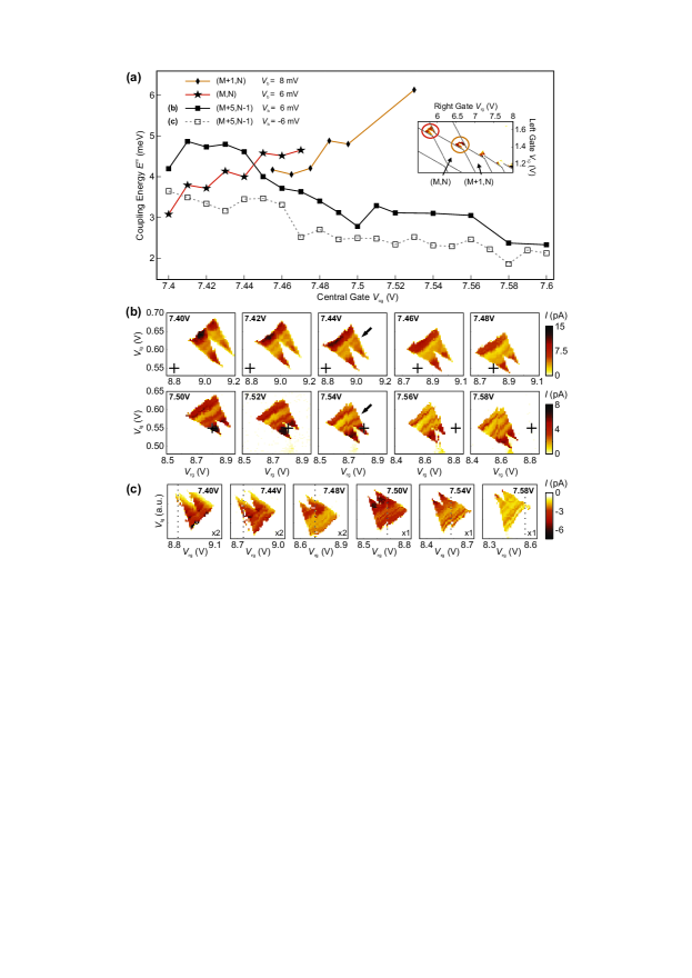
Since the absolute number of electrons in the two quantum dots are not known, we focus on relative changes and assume as a starting point M electrons in the right and N electrons in the left dot. For a near by triple point pair with one additional electron in the right dot (M+1,N) also a positive slope for versus is observed (see diamonds in Fig. 3(a)). However, for the triple point pair with (M+5,N-1) electrons the capacitive inter-dot coupling energy is decreasing as function of the central gate voltage (see full squares in Fig. 3(a)).
The corresponding triple point pairs from which the coupling energies have been extracted are shown in Fig. 3(b). With increasing central gate voltage the spacing between the triangle tips is decreasing, which is directly related to the decreasing capacitive coupling energy. A closer inspection of the excited states shows not only a coupling energy dependent reduction of the current within the triangles, but also a change in the coupling of the excited state with an
energy of 2 meV (see line running parallel to the base-line; highlighted by the black arrow). In the first row of Figure 3(b) the excited state resonance is almost completely suppressed and becomes more clear when increasing the central gate voltage (see second row). Due to capacitive cross-talk the overall position of the triple point pair changes in the left and right gate voltage plane as function of the central gate voltage. This is highlighted by the distance to the fixed black cross (+), which is fixed to the very same position in the gate voltage plane.
For a negative bias ( mV) the same dependence is observed (see open squares in Fig. 3(a) and Fig. 3(c)). Although the absolute value of the bias is the same, the trace with the open squares has an offset, compared to trace with the full squares. Please note that the corresponding triple point pairs (see Fig. 3(c)) nicely show the effect of the central gate on a charge rearrangement (see vertical dotted line). In the first two panels the rearrangement is located at the left edge of the triple point. With increasing central gate voltage the triple point pair is moving to lower right and left gate voltage values. For the rearrangement, which is located very close to the right barrier (vertical dotted line), the cross-talk is significantly lower and therefore it moves through the triangles and lies outside for central gate voltages above V.
Overall, we observe coupling energies ranging from about 2 meV to 6 meV. This is by a factor of 2 larger, compared to values from an earlier study on a single-layer double quantum dot mol09a . This difference might be explained by the considerably smaller size of the investigated quantum dots in our work.
More importantly we also observe a rather non-monotonic behavior of the capacitive coupling strength
as function of and (M,N). This is most
likely due to a disorder dominated electrostatic landscape in the narrow constriction
connecting the two quantum dots, which is in agreement with recent experiments on graphene
tunneling barriers gue11 .
III.3 Inter-dot Tunnel Coupling
Transport through the quantum dot states can be analyzed more quantitatively using the result from Stoof and Nazarov for resonant tunneling sto96 . In the limit of weak inter-dot tunnel coupling , where is the inter-dot tunnel coupling, and are incoming and outgoing tunnel rates, the current follows a Lorentzian line shape as a function of the detuning energy ,
| (2) |
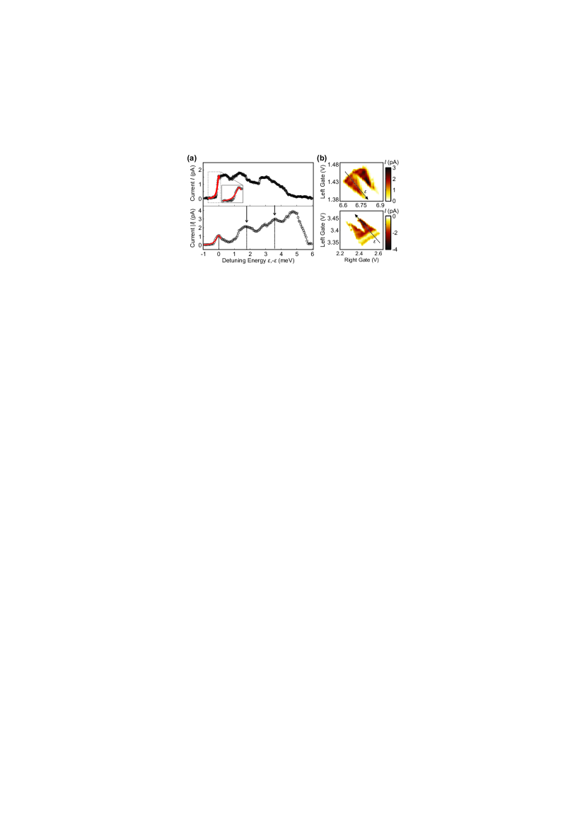
where is the Plank constant. In Figure 4(a) we plot two line-cuts along the detuning axis for
a positive and a negative bias ( 6 mV), and Lorentzian line fits to
the ground state lines.
Please note that in particular in the lower panel of Fig. 4(a) the excited states at an energy of 1.8 meV and
3.6 meV are nicely visible (see arrows).
The corresponding triple points with constant central gate voltages of V (upper panel) and V (lower panel) are shown in Figure 4(b).
Following Ref. liu10 the fitting is done only for the data points
outside of the bias triangle in order to minimize the contributions
from the inelastic transport.
We extract from the
fittings a tunnel rate from the right dot to drain and an inter-dot tunnel rate . From negative bias we obtain a tunnel rate from the left dot to source and an inter-dot tunnel rate .
These values are in reasonable agreement with the results reported by Liu et al. liu10 . The out of the dot tunnel rates have the same order of magnitude. The inter-dot tunnel rate, however, is in our case by a factor of six smaller (), which might be explained by the different device design. In their case the double dot is formed by two top gates on a 20 nm wide graphene nanoribbon. The tunneling barriers, induced and controlled by the 40 nm wide central gate, seem to be more transparent, compared to our side gated 30 nm wide constriction. Please note that the extracted inter-dot tunnel rate is also consistent with the upper bound of estimated by Molitor et al. mol10a for a single-layer graphene double quantum dot.
IV Conclusion
We have fabricated a bilayer graphene double quantum dot device, which can be tuned by a number of all-graphene lateral gates. The device has been characterized on a large energy range and its functionality is demonstrated by charge stability diagrams and well-resolved triple points.
We have studied the mutual capacitive inter-dot coupling energy and estimated the tunnel coupling energy . By varying the central gate voltage we are able to tune systematically from 2 to 6 meV which is in good agreement with former results for single-layer graphene double quantum dots mol10a ; liu10 , taking into account the smaller size of the presented quantum dots. Furthermore, the detailed investigation of individual triple point pairs has allowed to determine electronic excited state energies and an inter-dot tunnel rate of around which is roughly one order of magnitude lower, compared to recent results reported for single-layer graphene double dots mol10a ; liu10 . Most likely this difference might be due to the different device designs and architectures. However, further investigations and more statistics are needed to elucidate this issue.
In summary these results give insights into tunable bilayer graphene double quantum dot devices and the ability to tune the capacitive inter-dot coupling energy which is promising for the implementation of spin qubits in future graphene devices.
We thank A. Steffen, R. Lehmann and U. Wichmann for the help on sample fabrication and electronics. Discussions with J. Güttinger and S. Dröscher and support by the JARA Seed Fund and the DFG (SPP-1459 and FOR-912) are gratefully acknowledged.
References
- (1) B. Trauzettel, D.V. Bulaev, D. Loss, and G. Burkard, Nature Physics, 3, 192 (2007).
- (2) H. Min, J. E. Hill, N. A. Sinitsyn, B. R. Sahu, L. Kleinman, and A. H. MacDonald, Phys. Rev. B, 74, 165310 (2006).
- (3) D. Huertas-Hernando, F. Guinea, and A. Brataas, Phys. Rev. B, 74, 155426 (2006).
- (4) Z. Chen, Y.-M. Lin, M. Rooks and P. Avouris, Physica E, 40, 228 (2007).
- (5) M. Y. Han, B. Özyilmaz, Y. Zhang, and P. Kim, Phys. Rev. Lett., 98, 206805 (2007).
- (6) F. Molitor, et al., Phys. Rev. B, 79, 075426 (2009).
- (7) C. Stampfer, et al., Phys. Rev. Lett., 102, 056403 (2009).
- (8) K. Todd, et al., Nano Lett., 9, 416 (2009).
- (9) X. L. Liu, J. Oostinga, A. Morpurgo, and L. Vandersypen, Phys. Rev. B, 80, 121407 (2009).
- (10) P. Gallagher, et al., Phys. Rev. B, 81, 115409 (2010).
- (11) M. Y. Han, et al., Phys. Rev. Lett., 104, 056801 (2010).
- (12) B. Terrés, et al., Appl. Phys. Lett., 98, 032109 (2011)
- (13) C. Stampfer, J. Güttinger, F. Molitor, D. Graf, T. Ihn, and K. Ensslin, Appl. Phys. Lett., 92, 012102 (2008).
- (14) C. Stampfer, E. Schurtenberger, F. Molitor, J. Güttinger, T. Ihn, and K. Ensslin, Nano Lett., 8, 2378 (2008).
- (15) T. Ihn, et al., Materials Today, 13, 44 (2010).
- (16) J. Güttinger, et al., Appl. Phys. Lett., 93, 212102 (2008).
- (17) L. A. Ponomarenko, F. Schedin, M. I. Katsnelson, R. Yang, E. H. Hill, K. S. Novoselov, A. K. Geim, Science, 320, 356 (2008).
- (18) S. Schnez, et al., Appl. Phys. Lett., 94, 012107 (2009).
- (19) J. Güttinger, et al., Phys. Rev. B, 83, 165445 (2011).
- (20) L.-J. Wang, et al., Appl. Phys. Lett., 97, 262113 (2010).
- (21) F. Molitor, S. Dröscher, J. Güttinger, A. Jacobson, C. Stampfer, T. Ihn, and K. Ensslin, Appl. Phys. Lett., 94, 222107 (2009).
- (22) F. Molitor, et al., Europhys. Lett., 89, 67005 (2010).
- (23) X. L. Liu, D. Hug, L. Vandersypen, Nano Lett., 10, 1623 (2010).
- (24) L.-J. Wang, H.-O. Li, Z. Su, T. Tu, G. Cao, C. Zhou, X.-J. Hao, G.-C. Guo, and G.-P. Guo, arXiv:1011.5347 (2010).
- (25) C. Volk, S. Fringes, B. Terrés, J. Dauber, S. Engels, S. Trellenkamp, and C. Stampfer, Nano Lett., 11, 3581 (2011).
- (26) S. Schnez, F. Molitor, C. Stampfer, J. G ttinger, I. Shorubalko, T. Ihn, and K. Ensslin, Appl. Phys. Lett. 94, 012107 (2009).
- (27) J. Güttinger, T. Frey, C. Stampfer, T. Ihn, and K. Ensslin, Phys. Rev. Lett., 105, 116801 (2010).
- (28) J. Güttinger, C. Stampfer, F. Libisch, T. Frey, J. Burgdörfer, T. Ihn, and K. Ensslin, Phys. Rev. Lett., 103, 046810 (2009).
- (29) T. Mashoff, M. Pratzer, V. Geringer, T. J. Echtermeyer, M. C. Lemme, M. Liebmann, and M. Morgenstern, Nano Lett., 10, 461 (2010).
- (30) J. B. Oostinga, H. B. Heersche, L. Liu, A. F. Morpurgo, and L. M. K. Vandersypen, Nature Materials, 7, 151 (2008).
- (31) Y. Zhang, T. Tang, C. Girit, Z. Hao, M. Martin, A. Zettl, M. Crommie, Y. Ron Shen, and F. Wang, Nature, 459, 820 (2009).
- (32) K. S. Novoselov, A. K. Geim, S. V. Morozov, D. Jiang, M. I. Katsnelson, S. V. Dubonos, I. V. Grigorieva, A. A. Firsov, Science, 306, 666 (2004).
- (33) K. S. Novoselov, A. K. Geim, S. V. Morozov, D. Jiang, M. I. Katsnelson, I. V. Grigorieva, S. V. Dubonos, A. A. Firsov, Nature, 438, 197-200 (2005).
- (34) A. C. Ferrari, et al., Phys. Rev. Lett., 97, 187401 (2006).
- (35) D. Graf, F. Molitor, K. Ensslin, C. Stampfer, A. Jungen, C. Hierold, and L. Wirtz, Nano Lett., 7, 238 (2007).
- (36) F. Molitor, J. Güttinger, C. Stampfer, D. Graf, T. Ihn, and K. Ensslin, Phys. Rev. B, 76, 245426 (2007).
- (37) W. G. van der Wiel, S. De Franceschi, J. M. Elzerman, T. Fujisawa, S. Tarucha, and L. P. Kouwenhoven, Rev. Mod. Phys., 75, 1-22 (2002).
- (38) T. H. Stoof, Y. V. Nazarov, Phys. Rev. B, 53, 1050 (1996).