Manifestations of multiple-carrier charge transport in the magnetostructurally ordered phase of undoped BaFe2As2
Abstract
We investigated the transport properties of BaFe2As2 single crystals before and after annealing with BaAs powder. The annealing remarkably improves transport properties, in particular the magnitude of residual resistivity which decreases by a factor of more than 10. From the resistivity measurement on detwinned crystals we found that the anisotropy of the in-plane resistivity is remarkably diminished after annealing, indicative of dominant contributions to the charge transport from the carriers with isotropic and high mobility below magnetostructural transition temperature and the absence of nematic state above . We found that the Hall resistivity shows strong non-linearity against magnetic field and the magnetoresistance becomes very large at low temperatures. These results give evidence for the manifestation of multiple carriers with distinct characters in the ordered phase below . By analyzing the magnetic field dependences, we found that at least three carriers equally contribute to the charge transport in the ordered phase, which is in good agreement with the results of recent quantum oscillation measurements.
I Introduction
Parent compounds of iron-based superconductors undergo a tetragonal-to-orthorhombic structural transition upon cooling accompanied by an antiferromagnetic (AFM) order and show anomalous metallic behavior. Rotter In this ordered phase, spins align antiferromagnetically along the axis and ferromagnetically along the axis, Huang so the electronic state is essentially anisotropic. Recent in-plane resistivity measurements performed on detwinned crystals of Ba(Fe1-xCox)2As2, CaFe2As2, and SrFe2As2 Chu ; Tanatar ; Blomberg revealed an anomalous anisotropic electronic properties that the resistivity along the AFM spin direction with longer lattice constant ( axis) is smaller than the resistivity along the ferromagnetic (FM) spin direction with shorter lattice constant ( axis) and this in-plane resistivity anisotropy can be seen in the tetragonal phase well above the phase transition temperature , which has been discussed in terms of nematicity. Chu In relation to the nematicity, the orbital polarization above is observed by angle-resolved photoemission spectroscopy (ARPES). Yi1 However, the in-plane resistivity above is negligibly small in the cases of CaFe2As2 and SrFe2As2 which show a strongly first-order phase transition, Blomberg indicating that the in-plane resistivity anisotropy above or nematicity might not be intrinsic but could be induced by the external pressure.
The in-plane resistivity anisotropy of undoped BaFe2As2 is relatively small compared with underdoped Ba(Fe1-xCox)2As2, Chu despite the lattice orthorhombicity diminishes monotonically with increasing Co concentration. Prozorov The small anisotropy of undoped BaFe2As2 has been discussed from magnetotransport measurements in terms of a dominant role of isotropic and high-mobility Dirac pockets with the Dirac point near the Fermi energy , Huynh ; Kuo which were first observed by ARPES (the Dirac point is located at 1 5 meV from ). Richard However, several Fermi surface (FS) pockets other than Dirac pockets also exist in the ordered state as evidenced by ARPES Yi1 ; Yi2 ; Y.K.Kim and quantum oscillation. Terashima ; Analytis In such a multiple-band system, is it really possible that such tiny Dirac pockets with very small density dominate the charge transport? Additionally, recent optical measurement performed on detwinned BaFe2As2 crystal Nakajima2 revealed that almost isotropic Drude component existing along both and axis dominates the dc conductivity. The estimated Drude weight is of the order of 1020 cm-3, which seems too large to be formed only by tiny Dirac pockets. It seems that one needs another explanation for the small in-plane resistivity anisotropy of undoped BaFe2As2.
It is also reported that annealing remarkably improves transport properties in the ordered phase of BaFe2As2, Rotundu which indicates that the as-grown crystals contain appreciable amount of defects/impurities, and hence the observation of the intrinsic charge transport in this system might be inhibited. Therefore, it is required to investigate the intrinsic transport properties of this compound using annealed crystals.
In this paper, we present the transport measurements on BaFe2As2 single crystals with much improved quality. We show that the in-plane resistivity anisotoropy both above and below is diminished and the in-plane resistivity becomes almost isotropic, which indicates that the nematicity may not be intrinsic. We also provide clear evidence from the magnetotransport measurements that multiple carriers contribute to the charge transport in the ordered phase of BaFe2As2. Only tiny Dirac pockets do not play a dominant role as previously reported, but contribution to the conductivity from at least three types of carriers mask the underlying anisotropic electronic states.
II Experimental procedures
Single crystals of BaFe2As2 were grown by the self-flux method as described elsewhere.Nakajima1 The crystals were cut in a rectangular shape along the tetragonal [110] directions which become or axes in the orthorhombic phase. Typical crystal dimensions were 1.5 1.5 0.5 mm3 with the shortest edge along the axis. Part of the crystals were sealed into an evacuated quartz tube together with Ba or BaAs powders and annealed for several days. A standard four-terminal method was used for the in-plane resistivity measurements on twinned crystals. The magnetoresistance (MR) and Hall resistivity were measured with the electrical current along the plane and the magnetic field along axis. For detwinning, the BaFe2As2 crystals were set into an uniaxial pressure cell and detwinned by applying compressive pressure along the tetragonal [110] direction. Liang The resistivity along the and axis were measured simultaneously using Montgomery method Montgomery without releasing pressure. The measurements in the magnetic fields up to 7 T were performed in a Quantum Design physical property measurement system (PPMS). MR and in the magnetic fields up to 14 T were measured at the High Magnetic Field Laboratory, KYOKUGEN, Osaka University.
III Results and discussion
III.1 Annealing effect on in-plane resistivity
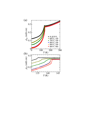
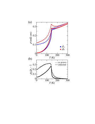
Figure 1(a) shows temperature () dependence of the in-plane resistivity () measured on twinned BaFe2As2 crystals annealed under various conditions. () of the as-grown crystal (black dots) shows typical temperature dependence so far reported for this compound. () drops at 136 K corresponding to the magnetostructural transition and shows residual resistivity of typically 0.1 mcm. The residual resistivity ratio () defined as (300K)/(5K) is about 3. Because the ordered state below has orthorhombic crystal structure, the twinned crystal has domains with different orientations hence the scattering at domain boundaries could be a source of residual resistivity. However, this is unlikely as a main source of scattering in the present case since () of detwinned BaFe2As2 still shows large residual resistivity (see dashed curves in Fig. 2(a)).
The annealing remarkably reduced the residual resistivity in the ordered phase of BaFe2As2 as reported in Ref. Rotundu . In general, the annealing process would remove crystal defects and lattice dislocations which are possible scattering sources and can cause large residual resistivity. Rotundu adopted low-pressure Ar gas annealing and obtained crystals with 36 after 30-day annealing at 700 oC. Rotundu In order to shorten the annealing time, we annealed crystals in a evacuated quartz tube together with Ba or BaAs powders since we assumed that the main sources of scattering are defects and/or dislocations of Ba and/or As sites. However, annealing with Ba is found to not much improve the crystal quality, since Ba reacts with crystals above 600 oC and gets worse. We found that can be improved more quickly by annealing with BaAs than Ar gas annealing. After annealing for 48 hours at 800 oC, we obtained crystal with 34. However, it is still unclear why of this compound is so sensitive to the annealing process.
Temperature dependence of () for the annealed crystal seems almost unchanged above after annealing, the annealing process scarcely affects the transport properties in the PM phase. On the other hand, as is shown in Fig. 1(b), increases from 136 K to 142 K and the phase transition becomes sharper probably because crystal defects are removed and it helps to stabilize the orthorhombic lattice and magnetic ordering. Remarkably, () drops much steeper below and goes down to 10 cm at = 5 K, one order of magnitude smaller than the value of as-grown crystal. If the carrier density is unchanged after annealing as reported, Rotundu this indicates that carrier mobility is greatly enhanced by annealing.
III.2 In-plane resistivity anisotropy
The in-plane resistivities of detwinned BaFe2As2 crystal are shown in Fig. 2(a). Note that effects of annealing on the in-plane resistivity anisotropy are also discussed by Nakajima, in Ref. Nakajima2 . The dashed line corresponds to resistivity components for the as-grown crystal. The blue and red colors correspond to resistivity along axis () and axis (), respectively. Around room temperatures there is no appreciable difference between and . As temperature is lowered, continues to decrease, while shows an upturn toward . The in-plane resistivity anisotropy can be seen well above , from about 80 K above, and is always smaller than . These results reproduce the reported ones Chu and confirm that the crystal is successfully detwinned by our technique. The in-plane resistivity anisotropy defined as /-1 is plotted in Fig. 2(b). The anisotropy shows a maximum value 0.33 just below , but it is robust even at the lowest temperature ( 0.2 at = 5 K).
The solid lines in Fig. 2(a) show the resistivity components of the annealed crystal. The temperature dependence of and seems qualitatively similar to that of the as-grown crystal. However, the anisotropy becomes appreciable only about 40 K above , that is, the phase transition becomes more first-order like as seen in SrFe2As2 and CaFe2As2. Krellner ; Ni This suggests that the magnetostructural transition might essentially be of the first order even in the purest sample of BaFe2As2. Therefore, the in-plane resistivity anisotropy above seems not originated from nematic phase but induced by the external pressure and/or remaining crystal defects/disorder. Remarkably, the anisotropy is much reduces as compared with that for as-grown crystal and diminishes as temperature is decreased below and the in-plane resistivity becomes nearly isotropic at temperatures well below (/-1 0.04 at 5 K). In fact, the isotropic charge transport at low temperatures is consistent with the results of other experiments. ARPES Yi1 ; Yi2 ; Y.K.Kim and quantum oscillation Terashima ; Analytis revealed ellipsoidal FS pockets which, when summed over the momentum space, would result in isotropic conductivity. Also, the optical conductivity spectra of detwinned BaFe2As2 for light polarization along and axis (measured crystals were annealed under the same condition) Nakajima2 are dominated by an isotropic Drude component with extremely high peak value (of the order of 105 cm-1 at = 5 K) and narrow width, consistent with the dc resistivity. The anisotropy in optical conductivity shows up in finite frequency region, which arises from anisotropic gap feature below . The question is, whether or not this Drude term originates from the tiny Dirac pockets. We will answer this after we show the results of magnetotransport measurements.
III.3 Magnetoresistance
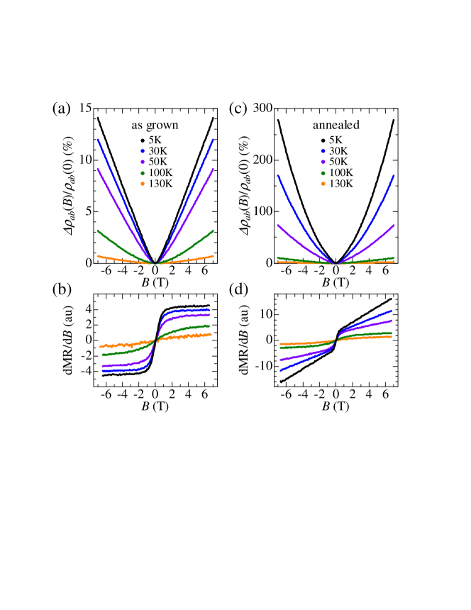
Figures 3(a)-(d) show the magnetic field () dependence of the magnetoresistance (MR) for transverse magnetic field (, ) and its derivative with respect to magnetic field for as-grown (a,b) and annealed (c,d) crystals, respectively. The magnitude of MR is defined as ()/(=0)=[()-(=0)]/(=0). In both cases, MR is smaller than 0.03 in the PM phase and rapidly increases below . MR of as-grown crystal is 14 at = 7 T and = 5 K (Fig. 3(a)) and shows almost -linear dependence above 1T, which is more clearly seen in the dependence of the derivative of MR (dMR/d) (Fig. 3(b)). -linear MR is anomolous, since in the framework of simple two carrier model, MR at low fields can be written in the form of ()2 where is magnetoresistance mobility, and MR saturates at high fields where or 1. Huynh ascribed this non-saturating linear MR to a quantum transport of Dirac cone states Huynh based on a model proposed by Abrikosov. Abrikosov However, recent study of MR for as-grown BaFe2As2 under higher magnetic field up to 50 T showed nonlinear but quadratic dependence of MR at high fields Yuan revealing the complicated dependence of MR.
In the case of the annealed crystal, MR reaches 280 at = 7 T and = 5 K (Fig. 3(c)), which is by an order larger than that of as-grown crystal. Furthermore, in contrast to the case of as-grown crystal, MR shows quadratic dependence up to 7 T. Considering that the magnitude of MR is a measure of carrier mobility, the mobility of carriers should be greatly enhanced by the annealing, which is consistent with the decrease of residual resistivity. Note that dMR/d has a kink-like structure at low field around 0.5 T, that is, MR of annealed crystal also has some -linear component similar to the case of as-grown crystal (Fig. 3(d)), suggestive of a contribution from Dirac pockets. However, observed large and quadratic -dependent MR gives evidence that other FS pockets have appreciable contribution to the charge transport in the ordered phase of BaFe2As2.
III.4 Hall effect
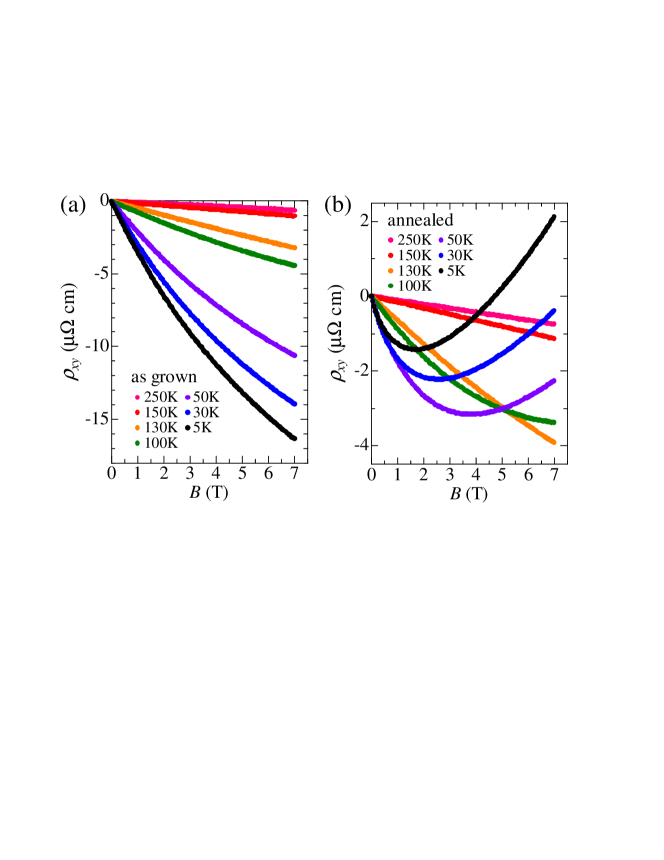
Figure 4(a) shows the magnetic field dependence of the Hall resistivity (, ) for as-grown crystal taken at several temperatures. () of as-grown crystal shows basically -linear dependence below and a deviation from the -linearity becomes apparent at well below . A previous report showed this sub-linear dependence of Hall resistivity persists to 50 T, Yuan which was ascribed to the dependence of carrier density.
The dependence of () for annealed crystal is shown in Fig. 4(b). In stark contrast to the as-grown crystal, () below soon deviates from -linear dependence and exhibits nonmonotonic dependence. Especially at = 5 K, () changes its sign to positive above 4 T. It is natural to attribute this dependence of () to the multiple-carrier effect. Intuitively, the negative sign of Hall coefficient at low field should be related to electrons with higher mobility and the positive sign at high field indicates the prevalence of hole carriers with relatively lower mobility.
Obviously, the magnitude of residual resistivity, the dependence of MR, and the nonmonotonic- dependence of are all correlated. They orginate from multiple-carrier contribution which becomes clear as the sample quality is improved or as the carrier mobilities become higher. Below, in order to make more quantitative analysis on these results, we apply a multiple-carrier model to ().
III.5 Multiple-carrier model analysis
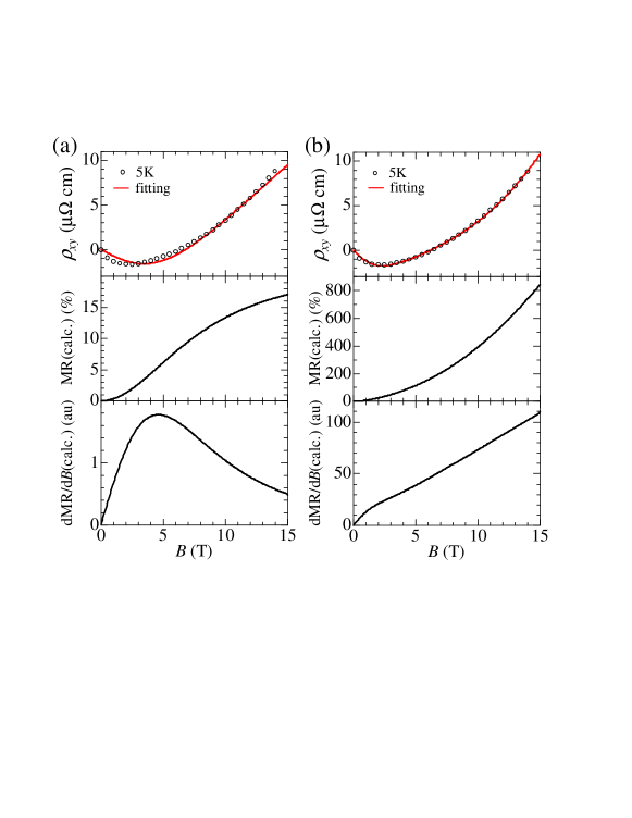
First, we used a simple two-carrier model fitting Chambers assuming one electron-type and one hole-type carriers. As is shown in the top panel of Fig. 5(a), the two-carrier model fairly well fits (). However, the fitting parameter set shown in Table 1 seems not reasonable, since (i) the density of holes is by two orders larger than that of electrons, inconsistent with ARPES Yi1 ; Yi2 ; Y.K.Kim and quantum oscillation Analytis ; Terashima , (ii) a calculated MR using the obtained parameter set is 15 at 14 T, much smaller than the experimental data ( 800 at = 14 T, see Fig. 6(b)), and (iii) the calculated MR shows saturating behavior which can be seen as decrease of dMR/d above 5 T (Fig. 5(c)). Any other parameter sets do not lead to better fitting than that shown in Fig. 5(a) (especially, if one put the constraint , fitting of () becomes worse). Thus, the two-carrier model is insufficient to describe the dependence of () and MR.
In order to explain the experimental data, we add a third carrier instead of considering -dependent carrier density and/or Dirac cone states, namely, we apply three-carrier model fitting. Chambers (see Appendix A) One needs a number of parameters (carrier type, electron or hole, carrier density and mobility for each carrier and their anisotropy) for three-carrier model fitting, but there are several constraints; (i) anisotropy would be negligible since the in-plane charge transport is almost isotropic, (ii) total carrier density should be of order of 1020 cm-3 as estimated from the Drude weight in the optical spectrum, Nakajima1 (iii) the densities of electrons and holes should be equal as is also confirmed by the angle-resolved photoemission spectroscopy (ARPES) Yi1 ; Yi2 ; Y.K.Kim and quantum oscillation data Terashima , and (iv) the obtained parameter sets should be consistent with the magnitude of resistivity and MR.
| carrier | 1 | 2 | 3 |
|---|---|---|---|
| type | (Dirac?) | ||
| (2 carrier) (1020cm-3) | 0.05(4) | - | 6(2) |
| (2 carrier) (103cm2/Vs) | 1.5(3) | - | 0.1(1) |
| (3 carrier) (1020cm-3) | 0.3(2) | 0.7(2) | 1.0(2) |
| (3 carrier) (103cm2/Vs) | 4.5(5) | 1.5(2) | 1.8(2) |
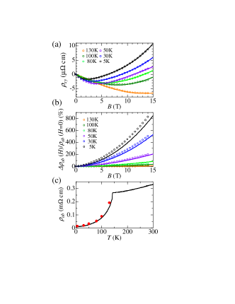
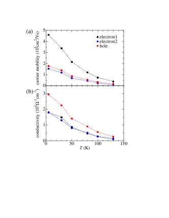
In Fig. 5(b), we show the fitting results for () at = 5 K. The obtained parameter sets are shown in the Table 1. From the result of fitting, we find a few important points. Firstly, () of annealed crystal best fits when we assume one type of electron with very high mobility () and smallest density (), another type of electron with relatively low mobility () and larger density (), and holes with the largest density () and mobility comparable to the 2nd electrons (). Secondly, it is possible to reproduce the temperature dependence of () by assuming reasonable temperature dependence of mobility for each carrier without changing the carrier density (Fig. 6). Thirdly, () of as-grown crystal best fits by suppressing the mobility of each carrier using the same carrier density obtained from the fitting for () of annealed crystal (see Appendix B). As is shown in Table 1 and Fig. 7, the three carriers have distinct characters each other but equally contribute to the charge transport.
III.6 Comparison with other experiments
One type of the electron carriers with highest mobility and smallest density we extracted from the present results is likely to be associated with electron FS pockets originating from Dirac-cone-like energy bands with the Dirac point at 23 meV below observed by ARPES measurements. Y.K.Kim Note that there are two types of Dirac-like pockets with different sizes in BaFe2As2 as observed by ARPES, Y.K.Kim and the Dirac-like pockets we consider here are larger ones, which are different from the tiny Dirac pockets whose dominant contribution to the charge transport has been discussed in previous reports. Huynh ; Kuo As for the 2nd electron and the hole FS pockets we suppose, they are actually observed by ARPES. Yi1 ; Yi2 ; Y.K.Kim The three types of carriers obtained in this study are in good agreement with the recent quantum oscillation measurement performed on annealed BaFe2As2 crystal. Terashima
Since all the three carriers have high mobility as is shown in Table 1 (even the lowest one, = 1.5 103 cm2/Vs at = 5 K), probably they together form a narrow Drude component in the optical conductivity spectra, Nakajima2 which is in contrast to the previous reports suggesting the dominant role of tiny Dirac pockets. Huynh ; Kuo
In fact, the dependence of MR, especially the linear dependence seen in as-grown BaFe2As2 case, cannot be explained even in the framework of three-carrier model using the same parameter sets obtained by analyzing . In order to explain this behavior, we probably need to include the fourth carrier, which might be electrons with very small density ( 1017 cm-3) and exclusively high mobility ( 104 cm2/Vs) perhaps originating from tiny Dirac pockets. However, the contribution, if any, to the conductivity from such pockets has to be small in the annealed samples, since the estimated conductivity ( 103 cm2) is much smaller than those of three types of carriers we obtained in this study (Fig. 7(b)).
IV Conclusions
We found that annealing BaFe2As2 crystals with BaAs is very efficient way to improve the quality of the crystals. Using those annealed crystals, we observed strongly non-linear dependence of Hall resistivity and huge quadratic -dependent magnetoresistance at low temperatures in the magnetostructurally ordered state. In order to understand these transport properties, we applied three-carrier, two types of electrons and one type of holes, model analysis and successfully reproduced the data quantitatively. These three types of carriers are in excellent agreement with recent quantum oscillation measurements made on similarly high-quality crystals. All the three carriers are found to equally contribute to the conductivity. From the measurements on detwinned crystals we found that the anisotropy of in-plane resistivity and its temperature range above diminish as the sample quality is improved by annealing. This suggests that the so far conceived nematic phase is not intrinsic but induced by external pressure, impurities or crystal disorder. Also, the in-plane resistivity is almost isotropic at temperatures well below , even though the electronic state in the ordered phase is essentially anisotropic as evidenced by the optical conductivity. In the ordered state, a radical reconstruction of the FS takes place with gap opening in some part of the FS. Remaining carriers / reconstructed FS - two electron FS and one hole FS pockets - in the ordered state have isotropic contribution to the charge transport and mask the anisotropic charge dynamics at higher energies.
Acknowledgments
We thank T. Terashima and N. Kurita for helpful discussions. SI and MN thank to the Japan Society for the Promotion of Science (JSPS) for the financial support. This work was supported by Transformative Research-Project on Iron Pnictides (TRIP) from the Japan Science and Technology Agency, and by the Japan-China-Korea A3 Foresight Program from JSPS, and a Grant-in-Aid of Scientific Research from the Ministry of Education, Culture, Sports, Science, and Technology in Japan.
Appendix
IV.1 Fitting procedure
The fitting procedure is shown below. According to the three-carrier model, J.S.Kim the Hall resistivity is given by
where
Note that and are the carrier density and mobility of -th carrier, respectively, and the sign of the carrier mobility is negative for electrons and positive for holes in the calculation.
IV.2 Three-carrier model analysis of Hall resistivity of as-grown BaFe2As2 crystal
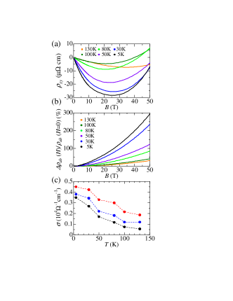
In Fig. 8(a), we show the results of three-carrier model fitting for the Hall resistivity of as-grown BaFe2As2 crystal in the magnetic field up to 50 T. Yuan Figure 8(b) shows the calculated MR using obtained parameter sets. We successfully reproduce those experimental data using three-carrier model, without introducing the dependence of carrier density. The mobility of each carrier is strongly suppressed compared with annealed BaFe2As2 crystal, but the carriers have almost equal contributions to the conductivity like in the case of annealed crystal (Fig. 8(c)).
| carrier | 1 | 2 | 3 |
|---|---|---|---|
| type | (Dirac?) | ||
| (1020cm-3) | 0.2(2) | 0.7(2) | 1.2(2) |
| (103cm2/Vs) | 1.1(3) | 0.3(2) | 0.2(2) |
References
- (1) M. Rotter, M. Tegel, D. Johrendt, I. Schellenberg, W. Hermes, and R. Pottgen, Phys. Rev. B 78, 020503(R) (2008).
- (2) Q. Huang, Y. Qiu, W. Bao, M. A. Green, J. W. Lynn, Y. C. Gasparovic, T. Wu, G. Wu, and X. H. Chen, Phys. Rev. Lett. 101, 257003 (2008)
- (3) J.-H. Chu, J. G. Analytis, K. De Greve, P. L. McMahon, Z. Islam, Y. Yamamoto, and I. R. Fisher, Science 329, 824 (2010).
- (4) M. A. Tanatar, E. C. Blomberg, A. Kreyssig, M. G. Kim, N. Ni, A. Thaler, S. L. Bud’ko, P. C. Canfield, A. I. Goldman, I. I. Mazin, and R. Prozorov, Phys. Rev. B 81, 184508 (2010).
- (5) E. C. Blomberg, M. A. Tanatar, A. Kreyssig, N. Ni, A. Thaler, Rongwei Hu, S. L. Bud’ko, P. C. Canfield, A. I. Goldman, and R. Prozorov, Phys. Rev. B 83, 134505 (2011).
- (6) R. Prozorov, M. A. Tanatar, N. Ni, A. Kreyssig, S. Nandi, S. L. Budko, A. I. Goldman, and P. C. Canfield, Pys. Rev. B 80, 174517 (2009).
- (7) K. K. Huynh, Y. Tanabe, and K. Tanigaki, Phys. Rev. Lett. 106, 217004 (2011).
- (8) H. H. Kuo, J.-H. Chu, S. C. Riggs, L. Yu, P. L. McMahon, K. De Greve, Y. Yamamoto, J. G. Analytis, and I. R. Fisher, Phys. Rev. B 84, 054540 (2011).
- (9) P. Richard, K. Nakayama, T. Sato, M. Neupane, Y.-M. Xu, J. H. Bowen, G. F. Chen, J. L. Luo, N. L. Wang, X. Dai, Z. Fang, H. Ding, and T. Takahashi, Phys. Rev. Lett. 104, 137001 (2010).
- (10) M. Yi, D. H. Lu, J.-H. Chu, J. G. Analytis, A. P. Sorini, A. F. Kemper, B. Moritz, S.-K. Mo, R. G. Moore, M. Hashimoto, W. S. Lee, Z. Hussain, T. P. Devereaux, I. R. Fisher, and Z.-X. Shen, Prc. Natl. Acad.Sci. USA 108 6878 (2011).
- (11) M. Yi, D. H. Lu, J. G. Analytis, J.-H. Chu, S.-K. Mo, R.-H. He, M. Hashimoto, R. G. Moore, I. I. Mazin, D. J. Singh, Z. Hussain, I. R. Fisher, and Z.-X. Shen, Phys. Rev. B 80, 174510 (2009).
- (12) Y. K. Kim, H. Oh, C. Kim, D. Song, W. Jung, B. Kim, H. J. Choi, C. Kim, B. Lee, S. Khim, H. Kim, K. Kim, J. Hong, and Y. Kwon, Phys. Rev. B 83, 064509 (2011).
- (13) J. G. Analytis, R. D. McDonald, J.-H. Chu, S. C. Riggs, A. F. Bangura, C. Kucharczyk, M. Johannes, and I. R. Fisher, Phys. Rev. B 80, 064507 (2009).
- (14) T. Terashima, N. Kurita, M. Tomita, K. Kihou, C. H. Lee, Y. Tomioka, T. Ito, A. Iyo, H. Eisaki, T. Liang, M. Nakajima, S. Ishida, S. Uchida, H. Harima, and S. Uji, arXiv:1103.3329.
- (15) M. Nakajima, T. Liang, S. Ishida, Y. Tomioka, K. Kihou, C. H. Lee, A. Iyo, H. Eisaki, T. Kakeshita, T. Ito, and S. Uchida, Prc. Natl. Acad.Sci. USA 108 12238 (2011).
- (16) C. R. Rotundu, B. Freelon, T. R. Forrest, S. D. Wilson, P. N. Valdivia, G. Pinuellas, A. Kim, J.-W. Kim, Z. Islam, E. Bourret-Courchesne, N. E. Phillips, and R. J. Birgeneau, Phys. Rev. B 82, 144525 (2010).
- (17) M. Nakajima, S. Ishida, K. Kihou, Y. Tomioka, T. Ito, Y. Yoshida, C. H. Lee, H. Kito, A. Iyo, H. Eisaki, K. M. Kojima, and S. Uchida, Phys. Rev. B 81, 104528 (2010).
- (18) T. Liang, M. Nakajima, K. Kihou, Y. Tomioka, T. Ito, C.H. Lee, H. Kito, A. Iyo, H. Eisaki, T. Kakeshita, and S. Uchida, J. Phys. Chem. Solids, 72, 418 (2011).
- (19) H. C. Montgomery, J. Appl. Phys. 42, 2971 (1971).
- (20) C. Krellner, N. Caroca-Canales, A. Jesche, H. Rosner, A. Ormeci, and C. Geibel, Phys. Rev. B 78, 100504(R) (2008).
- (21) N. Ni, S. Nandi, A. Kreyssig, A. I. Goldman, E. D. Mun, S. L. Bud’ko, and P. C. Canfield, Phys. Rev. B 78, 014523 (2008).
- (22) A. A. Abrikosov, Phys. Rev. B 58, 2788 (1998).
- (23) H. Q. Yuan, L. Jiao, F. F. Balakirev, J. Singleton, C. Setty, J. P. Hu, T. Shang, L. J. Li, G. H. Cao, Z. A. Xu, B. Shen, and H. H. Wen, arXiv:1102.5476.
- (24) R. G. Chambers, Proc. Phys. Soc. A 65, 903 (1952).
- (25) J. S. Kim, J. Appl. Phys. 86, 3187 (1999).
Figures
