Formal Verification of an Iterative Low-Power x86 Floating-Point Multiplier with Redundant Feedback
Abstract
We present the formal verification of a low-power x86 floating-point multiplier. The multiplier operates iteratively and feeds back intermediate results in redundant representation. It supports x87 and SSE instructions in various precisions and can block the issuing of new instructions. The design has been optimized for low-power operation and has not been constrained by the formal verification effort. Additional improvements for the implementation were identified through formal verification. The formal verification of the design also incorporates the implementation of clock-gating and control logic. The core of the verification effort was based on ACL2 theorem proving. Additionally, model checking has been used to verify some properties of the floating-point scheduler that are relevant for the correct operation of the unit.
Keywords: Floating-Point, multiplication, IEEE standard, theorem proving, ACL2.
1 Introduction
Machine-assisted formal reasoning has become an integral part of the verification strategy for many floating-point (FP) hardware designs. At AMD, FP hardware has already been formally verified for more than years [8, 10, 11, 12, 13, 14].
In this paper we describe the formal verification of an iterative, low-power x86 FP multiplier that has been designed from scratch for a new processor core. We also reiterated the verification effort for a second processor core that reused two instances of the design in slight variations with little verification overhead. A detailed description of the initial design is presented in [17]. The unit incorporates several new features and optimizations that cause a large number of corner cases in the design. Many of these corner cases would have been very difficult to cover based on only random or directed simulation. The goal of the complete coverage of all corner cases of the design, together with the novelty and complexity of the design, were the initial motivation for the formal verification of this implementation. The reuse of the verification effort for a second design generation has shown to be an additional benefit for this verification approach.
The core of our formal verification effort is based on ACL2 theorem proving [2]. The unit functionality has been specified behaviorally at RTL level in a designer-readable Verilog description [8]. For this specification we have also established equivalence to specifications from previous implementations of the same FP instructions. We built on an existing Verilog-to-ACL2 translation tool to make the design and the specification accessible in ACL2. We verify the design rigorously with all bit-level details and features of the RTL that is used for production. Additional refinements for the implementation of certain macros are locally shown to be logically equivalent at the implementation stage.
The FP multiplier supports x87 and SSE multiplication, reciprocal approximation, division, and square root instructions. Operands and results can have one of seven different formats (two SSE, three x87, and two internal), and the three x87 precisions can be different in the operands and in the result. All four rounding modes of the IEEE FP standard 754 [5] are supported in compliance with previous x86 implementations. The division and square root instructions are implemented based on a multiplicative algorithm with dedicated use of the multiplier hardware. Additional features for buffering, complementing, and normalizing intermediate results, for multiply-add and multiply-subtract operation of the multiplication array, and for the IEEE rounding of an approximate significand quotient or square root are included in the multiplier hardware in support of the division and square root operations. We do not discuss these additional features in this paper, and solely focus on the FP multiplication operation of the unit in this presentation.
Depending on the instruction and precision, FP multiplications in this unit have a latency between two and five clock cycles. In the significand path, the generation of the Booth-recoded partial products and their compression to a carry-save representation of the product takes between one and three iterations of the same stage using a rectangular -bit multiplier array. A result of this stage is fed back to the previous stage in redundant carry-save representation and added as two additional addends into the rectangular multiplier array. For the Booth recoding of the partial products, the result of the adder tree contains a carry bit that represents the combined effect of the sign corrections for all partial products. The carry-save feedback of the multiplier array may or may not contain contributions to this carry bit. The tracking and compensation of carries in the feedback path needs very careful consideration of all possible scenarios. This complicates writing cycle-based invariants for the partial-product accumulation stage. During the iterative partial-product accumulation, the representation of the intermediate result is already shortened towards the target precision by iteratively calculating a sticky and a carry bit to summarize the effect of the lower tail of the representation on the rounding computation. From the representation of the partially compressed exact sum, the rounded results are then determined in either one or two rounding stages. These rounding stages are implemented by operation and precision, and the implementation is organized in a way very close to having a separate rounding implementation per instruction type. The subtle differences in the rounding algorithms for the different instruction types significantly reduces the reuse of verification efforts between different rounding versions.
The fact that the calculation of a multiplication can block the partial-product accumulation stage for up to three cycles restricts the pipelining of the unit and requires the unit to be state-controlled. New instructions may be scheduled only when the accumulation stage is available. This condition needs to be ensured by the FP scheduler that is implemented as a separate entity external to the FP multiplier. We address the correctness of the scheduling of FP multiplication instructions to the unit with respect to the unit’s constraints as a separate verification effort. We have addressed this separate verification task with a different verification approach based on a commercial model-checking tool. We have used the definition of standard Verilog signals to build assume-guarantee relationships between assertions and assumptions in these two verification efforts.
The iterative nature of the implementation requires a cycle-based setup for the control bits of the stages. In addition, operands also need to be held appropriately to be available when they are needed (e.g., during the iterations of the partial-product accumulation stage). The design is controlling the clocking logic of the corresponding flops for this purpose. In the view of our RTL translation tool, this introduces additional clocks to the design. The implementation of clock-gating creates a similar situation. We deal with both cases by removing the additional clocks and translating them to the original clock in a pre-processing step of the translation tool. The clock gating logic is often dependent on reset and requires inductive proofs. Because some of the clock-gating is implemented hierarchically, the corresponding inductive proofs also had to be conducted hierarchically.
The design and the formal verification of this unit largely did not occur concurrently. The design was almost completed by the time the formal verification effort was started. The advantage of this setting was that the design was very stable and the verification effort had to go through very few design modifications. One of them was the addition of a part of the clock gating logic. But this also means the design effort was not constrained by the formal verification effort, and the design had not been structured to simplify modular and hierarchical specification and the application of formal verification. This created more effort for the verification.
The formal specification and verification of the unit led to a deeper understanding of the properties of the implementation and its operation. This understanding allowed us to propose several improvements to the unit that were inspired by the formal verification of some of the properties of the unit. At least four of these optimizations have been realized in the current implementation. These improvements allowed removal of some logic from the design, reducing some critical delays in the implementation.
In Section 2 we describe our formal verification flow. In Section 3 we describe the formal specification of the unit. In Section 4 we describe some details of the FP multiplication implementation and highlight some verification challenges. In Section 5 we summarize our results before we conclude in Section 6.
2 Verification Flow

The core of our verification is based on ACL2 theorem proving [2]. Our ACL2 based verification flow is illustrated in Figure 1. To verify the RTL implementation, we need to translate both the multiplier RTL and the multiplier specification from Verilog to ACL2 logic. We use the formalization from [8] for the translation and build on an existing translation tool. Just a few small extensions were necessary for the translation tool to handle a few new features of the Verilog dialect used in this project. We made a few more changes to the translation process to deal with module dependencies more efficiently and to handle the translation of a large number of RTL modules faster.
As a result of the translation, Verilog wires and registers are translated to function definitions in ACL2 that maintain the signal name as the function name and that depend on a cycle parameter n. Verilog bit vectors are translated to integer-valued ACL2 functions, and the translation process also generates for each signal an ACL2-verified property on its bit width as expressed by its value range. The formalization is supported by the ACL2 RTL library [14] that has been developed during previous ACL2 verification projects at AMD and that is part of the public ACL2 distribution. Functions to extract, concatenate, or manipulate bits and bit vectors, and functions for logical operations, as well as a large set of verified properties and lemmas, are provided in this library in more than function definitions and theorems.
In the translation, Verilog assignments are translated using the logic definitions of the RTL library that correspond to the logic from the Verilog assignment from the signal definition in Verilog. The translation process works in several stages. An early, more direct translation is simplified in a later processing step and the equivalence of the two translations is proven in ACL2 [7]. ACL2 functions for wire definitions relate to the signals on which they depend in the same cycle. ACL2 functions for register definitions for cycle n relate to signals from the previous cycle n-1 or the current cycle n.
The translation of a wire
assign imm1 = in1 | (in2 & in3);
results in the following ACL2 function definition for imm1:
                       (DEFUN imm1 (n)
                              (LIOR (in1 n)
                                    (LAND (in2 n) (in3 n)
                                          1)
                                    1))
The translation of a register assignment
                       always @ (posedge clk)
                         out1  <=  in2
results in the following ACL2 function definition for out1:
                       (DEFUN out1 (n)
                              (if (zp n)
                                  (reset ‘out1 1)
                                  (in2 (- n 1))
                                  ))
In this translation process, all signals are related to the common ACL2 clock n. For the treatment of gated and modified clocks, we consider a pre-processing step that translates all Verilog clocks to one common Verilog clock, so the translation would only contain one common ACL2 clock parameter n. For a gated clock gclk = gcond & clk and its application to the assignment of gout1:
                       always @ (posedge gclk)
                         gout1  <=  in1;
our clock translation results in the following conditional statement using the common clock:
                       always @ (posedge clk)
                         if (gcond)
                            gout1 <= in1;
The translation of our multiplier RTL takes about minutes. This time only needs to be spent once after each modification of the design or the specification file to create the corresponding certified ACL2 model. To work on theorems using the ACL2 model, the certified model file can be loaded into ACL2 in a matter of seconds.
3 Formal Specification
The functionality of the unit we target is the computation of FP multiplications. The unit supports a variety of different multiplication options and a variety of other operations like divisions and square roots. The input of an opcode and an active enable bit indicates to the unit to start calculating on the operation represented by the opcode.
The different operations supported by the unit have different latencies. FP multiplications take two clock cycles for packed and scalar SSE SP operation, four clock cycles for SSE DP operation and five clock cycles for all other FP multiplications.
We would like to state as the functional specification that, if we observe the opcode of a five-cycle multiplication in cycle n with an active enable signal, the results of this instruction would be available after cycle n+4.
                  (Opcode(n) == ‘FMUL5) & enable(n)
                              ==>
                  FPM.out(n+4) == FPM5spec.out(FPM.in(n))
This is our ultimate verification goal for the five-cycle FP multiplications, and this is what we ultimately show. But this property is not a property of just the FP multiplier. The unit relies on the external FP scheduler to meet some requirements and to drive appropriate control signals to the unit. The FP scheduler needs to avoid scheduling new instructions when the unit is busy in iterations in its first stage and cannot accept the issue of new instructions, or when the schedule of the new instruction would lead to contention at the result bus of the unit, because two instructions in the unit would finish their calculations in the same cycle. We deal with the constraints for the FP scheduler in a separate verification effort outside of ACL2 and reformulate the unit functionality to remove the scheduling constraints. For this purpose, we express the unit functionality from the observations at its outputs and consider how these outputs have been computed. For the output observation in cycle n, it could be either that two cycles ago, a two-cycle multiplication had been started, or four cycles ago, a four-cycle multiplication had been started, or five cycles ago a five-cycle multiplication had been started. The following statement describes these conditions:
 if ((Opcode(n-1)==‘FMUL2) & enable(n-1))
      FPM.out(n) == FPM2spec.out(FPM.in(n-1))
 else if ((Opcode(n-3)==‘FMUL4) & enable(n-3) & ~enable(n-2))
      FPM.out(n) == FPM4spec.out(FPM.in(n-3))
 else if ((Opcode(n-4) == ‘FMUL5) & enable(n-4) & ~enable(n-3) & ~enable(n-2))
      FPM.out(n) == FPM4spec.out(FPM.in(n-4))
This statement implicitly defines a priority for two-cycle FP multiplications over four- and five-cycle multiplications and for four-cycle multiplications over five-cycle multiplications, and removes any additional scheduling constraints at the same time. This specification statement can be shown for the FP multiplier unit. Together with the external properties derived for the scheduler, it can then result in the ultimate verification target from further above.
In the code statements, we used some notation that is supposed to improve readability and represent our high-level view on the verification task. The equations combined Verilog-like syntax with the cycle parameter n from the ACL2 translations. The specification we work with in our design is written in Verilog syntax readable to designers. The Verilog specification has a few extensions allowed to define rational valued registers and to use certified functions for the specification of IEEE-specific rounding definitions [14]. These extensions are used to simplify and improve specification of IEEE FP functionality.
To deal with delays in our Verilog specification, we define delayed registers for all inputs to the unit. If we relate enable to the value of enable(n) in cycle n and assign
                       always @ (posedge CLK) begin
                         enable_D1 <= enable;
                         enable_D2 <= enable_D1;
                         enable_D3 <= enable_D2;
                         enable_D4 <= enable_D3;
                       end
we get the corresponding values for enable(n-1) to enable(n-4) in enable_D1 to enable_D4.
The arithmetic definition of the result values of the specification involves several steps:
-
1.
Extract the operand bits from register or memory format of the input operands to the sign, exponent, and significand fields and indications of special values.
-
2.
Define the rational values of the operands.
-
3.
Define the exact, unrounded (rational) operation result.
-
4.
Define the IEEE operation result of the appropriate target precision and rounding mode using parameterized IEEE rounding functions.
-
5.
Check for value ranges and exception conditions.
-
6.
Calculate the register format representation of the result.
-
7.
Select the correct case for the specification result.
An example of the definitions of rational FP operand values, of an unrounded, and of an IEEE-rounded result according to Steps to is given in the following:
                 always @* begin
                   ValA = (-1) ** SignA * MantA
                          * 2 ** (ExpA - (2 ** 17 - 1) - 67);
                   ValB = (-1) ** SignB * MantB
                          * 2 ** (ExpB - (2 ** 17 - 1) - 67);
                   ValUnrnd  =  ValA * ValB;
                   case (RND_MODE[1:0])
                     ‘RN:  ValRnd  =  $Near(ValUnrnd,  Prec);
                     ‘RM:  ValRnd  =  $Minf(ValUnrnd,  Prec);
                     ‘RP:  ValRnd  =  $Inf(ValUnrnd,   Prec);
                     ‘RZ:  ValRnd  =  $Trunc(ValUnrnd, Prec);
                   endcase
                 end
The final specification statement in the FP multiplier specification is written as an assert statement, which is translated into an ACL2 theorem. The main verification target for the ACL2 verification of FP multiplication is to verify this main theorem. Additional theorems are targeted for exception signals and other output results of the unit.
The Verilog specification for the FP multiplications is largely simplified by the behavioral features of the enhanced Verilog language and the availability of parameterized definitions for IEEE-specific functions (e.g., the use of the function $Near in extended Verilog for the specification of IEEE rounding in rounding mode round-to-nearest by the function near from the ACL2 RTL library). The writing of the specification for a larger set of x86 functions with the goal to match the functionality of previous x86 implementations of the same instructions can still be an error-prone task.
We had the specification of previous x87 and SSE FP multiplication implementations available in ACL2 for the design from K7/K8 [10]. Writing our specification in the same structure and using the same functions and definitions from the previous specification, so our Verilog specifications would match the previous ACL2 specifications after Verilog-to-ACL2 translation, helped us increase confidence in the specification and in the backwards compatibility of our verification target.
Our specification applied to any design evolution that we have considered. Clock-gating did not change any of the functional behavior that was specified for the design. Only the theorems and proofs of properties local to the unit had to be adjusted to incorporate the features of the additional clock-gating logic.
4 FP multiplier implementation
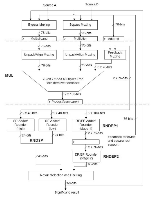
In this section we describe some details and features of the FP multiplier implementation. More details of the implementation can be found in [17]. A block diagram of the FP multiplier illustrating the details of the significand datapath is shown in Figure 2. To simplify this diagram, the additional hardware for exception processing, exponent computations, and divide/square-root support is not shown.
The significand datapath consists of three pipeline stages. The first pipeline stage consists of a -bit multiplier that uses modified radix- Booth recoding and a partial-product reduction tree consisting of compressors. The -bit multiplier accepts a feedback product in redundant carry-save form to facilitate iteration and a -bit addend that can be added to the product or subtracted from the product specifically to support divide and square-root operations. The addend is needed because the iterations for divide and square root use a restricted form of the multiply-add operation during iterations. The operand width of bits is required at the micro-architectural level to support division at the internal precision of bits that is needed for transcendental functions. The second and third pipeline stages consist of combined addition and rounding followed by result selection, formatting for different precisions, and forwarding of the result to the register file and bypass networks.
There are two identical copies of the SP rounding unit to support packed SP multiply operations and a single combined DP/EP rounding unit that also handles all rounding for divide and square-root operations. The SP rounders take one cycle and the DP/EP rounder takes two cycles. The outputs of the two SP rounders are combined, formatted, and multiplexed with the output from the DP/EP rounder to form the final result. The final result is written to the register file and forwarded back to the inputs of the FP multiplier and other FP units via the bypass networks to enhance performance of dependent operations. With such a configuration, a scalar SP multiplication takes one iteration, two parallel (packed) SP multiplications take one iteration, a scalar DP multiplication takes two iterations, and a scalar EP multiplication takes three iterations.
The significand multiplier consists of a -bit rectangular tree multiplier, which performs -bit multiplications over multiple cycles. This saves considerable area compared to a fully parallel -bit multiplier, but penalizes the performance of the higher precision (DP and EP) multiply instructions because the multiplier must stall subsequent multiply instructions. However, the multiplier is fully pipelined for SP operations.
The multiplier accepts a -bit multiplicand input, a -bit multiplier input, and a -bit addend input. These inputs are held for the duration of the operation. The -bit multiplier input is supplied to alignment multiplexing, which outputs two -bit values. Each -bit value is then recoded using a set of modified radix-4 Booth encoders. Two separate -bit multiplier values are required to support the packed SP mode.
The outputs of the Booth encoders are used to select the multiples of the multiplicand to form fourteen -bit partial products. One of the -bit multiplier values controls the generation of the upper bits of each partial product while the other -bit multiplier value controls the generation of the lower bits of each partial product. In non-packed modes, the two -bit multiplier values are identical.
In parallel to the partial-product generation, two -bit feedback terms are combined with a -bit addend using a carry-save adder. The carry-save addition is computed in parallel with the Booth encoding and multiplexing and does not add to the critical path. The 14 partial products plus two combined terms are summed using a compression tree consisting of three levels of compressors to produce a -bit product in redundant carry-save representation. The -bit carry-save product is then stored in two -bit registers. A diagram of the partial-product array for the -bit multiplication is show in Figure 3. This diagram also shows the alignment of the two -bit feedback terms and the -bit addend. The two feedback terms are needed to support iterations and are aligned to the right. The addend is needed to support division and square root and is aligned to the left.
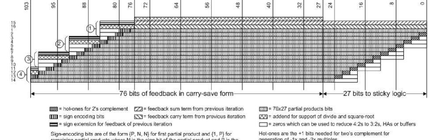
To avoid unnecessary hardware, the additional terms are inserted into the unused portions of the array wherever possible. This makes the hardware more efficient, but also more irregular, and it adds the complexity of having to decompose and recombine several bits and bit fields in the formulation of properties during verification. The ACL2 RTL and arithmetic libraries do not handle a large amount of these bit manipulations very efficiently. Figure 3 also shows how the partial-product terms are partitioned into groups of four corresponding to the first level of compressors. Although the multiplier is unsigned, a sign extension term is required to accommodate the sign embedded in the uncompressed feedback terms from the previous iteration. This is an artifact of the signed nature of the Booth encoding and the use of sign encoding of each individual partial product. The two feedback terms and addend are compressed using a carry-save-adder (CSA) into two terms, for a total of sixteen values to be summed.
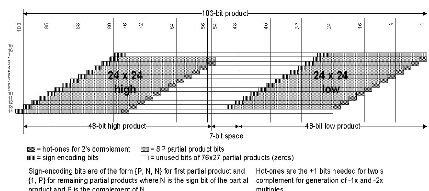
To support two parallel SP multiplications, the two SP multiplications are mapped onto the array simultaneously. The superposition of two -bit multiplier partial-product arrays onto a -bit partial-product array is shown in Figure 4. Because the lower array ends at bit , the significant bits of the upper array and lower array are separated by seven bits. The reduction tree has three levels of compressors. The width of the split between the upper and the lower part has been justified by the designers by the number of levels of compressors and based on how many bit positions a carry can travel at most per level. Based on this reasoning, no additional hardware had been added to kill any potential carries propagating from the lower array into the upper array. This kind of bit-level justification has also been used at some other parts of the design. It has caused the design to have some dependencies between module-level behavioral features and bit-level implementation details of low-level modules. These dependencies have made it more challenging to specify the implementation in a clean, modular fashion.
To accommodate the sign encoding bits and the hot-ones, an additional multiplexer is inserted after the Booth multiplexers and prior to the compressor tree. The multiplexing after the Booth multiplexing is only required for the sign encoding bits of the lower array and the hot-ones of the upper array, so the additional hardware required is small. This hardware, however, is on the critical path and adds the delay of a multiplexer.
For each multiply iteration of the iterative multiplication algorithm, the appropriate multiplier bits are selected for the high and low multiplier values and the product is computed in redundant carry-save form. For SSE-SP multiplies and the first iteration of all other precisions, the two feedback terms are set to zero. For the second iteration of SSE-DP multiplies and the second and third iterations of EP multiplies, the two feedback terms are set to the upper bits of the product from the previous iteration and are then added to the lower bits of the current product. SP multiplies require only a single iteration, DP multiplies require two iterations, and EP multiplies require three iterations.
The rounding circuitry takes as input the product in redundant carry-save form and rounds the result according to the given rounding mode. The rounding circuitry contains separate rounding units for SSE-SP high and SSE-SP low results, and a combined rounding unit that rounds for SSE-DP, x87-EP, and divide/square-root results. Each of the rounding units is based on a compound adder rounding scheme. The micro-architecture requires that the FP multiplier be able to produce the unrounded, normalized result for support of denormalized results. This complicates the use of injection-based rounding, which could have simplified the rounding units and their verification, because this would be closer to an available formalization of IEEE rounding in the ACL2 RTL library [14].
The SSE SP rounder performs SSE single-precision rounding only. This is a highly optimized and compact rounder compared to the DP/EP rounder because it only has to deal with one precision. This unit has two identical instances: one for the lower SSE-SP result and one for the upper SSE-SP result. In the SP rounding scheme, the upper 25 bits are passed through one level of half-adders before applying the compound adder. Initially, the design had implemented two levels of half-adders for this compression. The formal analysis revealed that the upper bound for the bits that are involved in the calculation of the LSB of the rounded significant were smaller by one than assumed by the designers. This allowed the removal one of the half-adder lines from the design without adverse effects. This is one of the optimizations that we referred to as inspired by the formal verification effort.
The combined DP/EP rounder performs rounding for SSE-DP, x87-SP, x87-DP, x87-EP, IP68 (for transcendental functions), and divide and square-root operations. Due to the large number of different precisions that must be supported, the DP/EP rounder is split over two cycles. The combined DP/EP rounder is based on a compound adder rounding scheme. It has some similarities with the SP rounding scheme, except it is necessary to perform a right shift to pre-align the rounding point to the same significance prior to the compound addition and to perform a left-shift to post-align the MSB to the same significance after the compound addition. This is the overhead for having to support multiple rounding points in the same datapath.
The second difference is that the carry tree and sticky logic need to include the carry-out and sticky from previous iterations.
The third difference is that for each target precision there is a pair of 2-1 multiplexers that are used to insert the two rounded LSBs into the correct positions within the final rounded significand.
The fourth difference is that for DP/EP operation, double significand overflows can occur during rounding. The DP/EP needs to be able to detect them, while the SP rounder can simply neglect any carries beyond position . For the DP/EP rounder, it is important to be careful to avoid any additional carry that could be contained in the -bit carry-save representation that is fed into the rounder. The non-existence of such carry is also a property that makes assumptions among several module boundaries and is only justified by bit-level details of the compressor implementations. The DP/EP rounder also provides a bypass path for divide and square root to allow the compound adder to be reused for other additions, such as computing the intermediate quotient ULP, instead of adding dedicated hardware.
To conclude the description of the design, we would like to point out a few selected challenges from this verification effort. The implementation of the unit was new and the design had largely been completed by the time the formal verification effort started. While the stability of the design was an advantage for verification, the fact that it was hard to justify any changes to the design to simplify the specification and verification effort created some challenges.
The designers were very helpful in explaining features of the design, but their knowledge of details and signal correlations to specify cycle- and bit-accurate constraints for the operation of some sub-modules was limited. Some of these constraints had to be determined experimentally in some iterations.
A particular cause for complexity in the specification of some modules and the proof of the corresponding properties was the high degree of optimization in the implementation. The optimizations made several high-level properties dependent on bit-level details of the design. Particular examples are the carry correction logic of the redundant feedback in the adder tree iterations, a subtle difference in the calculation of the significand overflow detection for rounding versus the selection of the corresponding exponent adjustment, the iterative sticky and carry computation with logic spread over different modules, the double significand overflow detection, and the hierarchy of clock-gating logic that is dependent on reset.
While these features help improve the performance and lower the power of the design, they also complicate modular specification and formal verification with our ACL2 theorem proving-based approach.
The design from this presentation has been reused for a second processor core in two instances with slight modifications. The main changes in one of the instances were related to variations in the implementation of clock-gating and the change of latencies and types of other instructions that could be handled concurrently by the unit. The main changes in the other instances involved the removal of RTL logic for a more efficient implementation of a subset of the original unit’s functionality. The adjustment of the verification effort to the modified unit instances required significantly less effort than the original verification. But all modifications were made more complex by the properties that were not modularized and spread over module hierarchies and boundaries. The concurrent instruction constraints and the clock-gating conditions could have been handled more efficiently in the updated instances if their properties had been better encapsulated and kept local in the original theorem formulations.
5 Verification Results
As the main result, the ACL2 verification effort has verified the main theorem from the Verilog specification of the unit and shown that the functionality of the implementation meets the FP multiplication specification from K7/K8. In the verification of this unit, we have made use of the ACL2 RTL and arithmetic libraries, but we also had to interactively develop and prove new custom theorems and function definitions in about lines of LISP in files.
The time to translate the design RTL and Verilog specification to ACL2 is about minutes; the time to certify the new theorems is about hours on a single machine and about six hours when using multiple machines.
The design had undergone a few modifications during the verification effort. Most of them were small and local, so it took only several days to adjust the theorems and proof hints to the design changes. One larger design change was the addition of an additional level of clock-gating to some parts of the design. This change required a significant modification in the assumptions and invariants of several sub-units, and adjusting the theorems and proof hints to work with the changes took a few months.
A significant number of theorems from the ACL2 verification effort could be shown by generating some of them in a more automated way, especially for parts of the control logic and bit-level features of the compressors. A main area for this are the properties that are implied by control bits of the unit that have fixed values for a specific cycle and a specific operation mode. The propagation of these constants through the logic and the simplification of expressions and theorems based on these constants were needed in multiple parts of the verification effort. In the past, we have looked into generating properties of such propagations automatically for the case that the values are constant during all cycles of the operation, but we have not adjusted this approach for the case that independent propagations and properties, that are not generally valid, are to be explored for individual cycles of the operation. The previous effort had used byproducts of the Verilog-to-ACL2 translation process to generate properties in ACL2 theorems that were then proven automatically. One way to extend this approach for cycle dependent properties could be based on unrolling the logic for the latencies of the operations, so that the properties would become cycle independent. Another approach could be based on the use of more automatic features of the ACL2 theorem prover like generating computed hints based on the propagated control values. The serious exploitation of these strategies did not fit into the schedule of this verification project, but will be considered for future ACL2-based verification at AMD.
To resolve the control and scheduling constraints for the FP multiplier, we have used a commercial model-checking tool by Jasper Design Automation. The main effort in this part of the project was the reduction of the logic in the cone of influence of the assertions. We interacted with our RTL designers for feedback on the interface constraints and dependencies in the FP scheduler. For the remaining set of interface signals, we applied exhaustive exploration to discover the dependency of the assertions on the interface signals. This helped us first to increase the depth of the search of the model checker, and finally to complete the proof of the assertions.
It is hard to specify any absolute time requirement for this part of the project because the interaction with the model checker was run as a side project to the ACL2 verification for a larger part of the project duration.
6 Conclusions
We have discussed the formal verification of a state-of-the-art low-power x86 FP multiplier implementation. The unit has been specified behaviorally in Verilog to match the functionality of previous x86 multiplication implementations. The multiplication implementation has been rigorously verified with all logic-level design details including clock-gating, unit control, and the scheduling of concurrent instructions. In this respect we have advanced the breadth, rigor, and complexity of the formal verification for our design and its environment compared to previous FP multiplication verification efforts to the extent that their efforts are revealed in the literature (e.g., [3, 4, 6, 9, 15, 16]). The design has also incorporated several new design features like the signed redundant iterative additive multiplier feedback that, to the best of our knowledge, have not previously been implemented or formally verified in production-level RTL for a commercial FP unit implementation.
The deeper understanding of the design that was gained from the verification process during specifying and proving design properties has shown to be very beneficial for the current design in identifying several improvements for the unit. We have also found that the verification effort could be modified to variations of the design. In two new instances of the unit that included small variations of the design, the formal verification effort could be reused with reasonable overhead for adjustments. Better understanding of the challenges of the verification process for this unit and the two modified instances will also help make future design and verification iterations more efficient and help identify areas of the verification process to be targeted for improved automation.
References
- [1]
- [2] ACL2 Web site. http://www.cs.utexas.edu/users/moore/acl2/.
- [3] Mark D Aagaard & Carl-Johann H Seger (1995): The formal verification of a pipelined double-precision IEEE floating-point multiplier. In: International Conference on Computer Aided Design, pp. 7–10.
- [4] Christoph Berg & Christian Jacobi (2001): Formal Verification of the VAMP Floating Point Unit. In: CHARME 2001, volume 2144 of LNCS, pp. 325–339, 10.1007/3-540-44798-9_26.
- [5] Institute of Electrical and Electronics Engineers (1985): IEEE Standard for Binary Floating-Point Arithmetic. ANSI/IEEE Standard 754-1985. IEEE, New York.
- [6] Roope Kaivola & Naren Narasimhan (2002): Formal Verification of the Pentium 4 Floating-Point Multiplier. In: Conference on Design, Automation and Test in Europe (DATE), pp. 20–27.
- [7] Matt Kaufmann (2003): A Tool for simplifying files of ACL2 definitions. In: Proceedings ACL2 Workshop. Available at: http://www.cs.utexas.edu/users/moore/acl2/workshop-2003/.
- [8] Matt Kaufmann, David Russinoff, Eric Smith & Rob Sumners (2005): Formal Verification of Floating-Point RTL at AMD Using the ACL2 Theorem Prover. In: 17th IMACS World Congress:Scientific Computation, Applied Mathematics and Simulation. Available at: http://www.russinoff.com/papers/paris.html.
- [9] Erik Reeber & Jun Sawada (2006): Combining ACL2 and an automated verification tool to verify a multiplier. In: International Workshop on the ACL2 Theorem Prover and its Applications, pp. 63–70, 10.1145/1217975.1217990.
- [10] David M. Russinoff (1998): A Mechanically Checked Proof of IEEE Compliance of a Register-Transfer-Level Specification of the AMD-K7 Floating-Point Multiplication, Division, and Square Root Instructions. LMS Journal of Computation and Mathematics 1, pp. 148–200.
- [11] David M. Russinoff (1999): A Mechanically Checked Proof of IEEE Compliance of the AMD K5 Floating-Point Square Root Microcode. Formal Methods in System Design 14, pp. 75–125, 10.1023/A:1008669628911.
- [12] David M. Russinoff (2007): A Mathematical Approach to RTL Verification. In: 19th International Conference on Computer Aided Verification, 10.1007/978-3-540-73368-3_2. Available at: http://www.russinoff.com/papers/cav/.
- [13] David M. Russinoff (2009): A Mechanically Verified Commercial SRT Divider. In: Design and Verification of Microprocessor Systems for High-Assurance Applications, Springer, pp. 23–63.
- [14] David M. Russinoff & Arthur Flatau (2000): Mechanical Verification of Register-Transfer Logic: A Floating-Point Multiplier. In: Computer-Aided Reasoning: ACL2 Case Studies, Kluwer, pp. 201–232.
- [15] Anna Slobodová, Jared Davis, Sol Swords & Warren Hunt (2011): A Flexible Formal Verification Framework for Industrial Scale Validation. In: Formal Methods and Models for Codesign (MEMOCODE), pp. 89–97, 10.1109/MEMCOD.2011.5970515.
- [16] Anna Slobodová & Krishna Nagalla (2004): Formal verification of floating point multiply add on Itanium processors. In: Fifth International Workshop on Designing Correct Circuits, ETAPS, pp. 144–156.
- [17] Dimitri Tan, Carl Lemonds & Michael J. Schulte (2009): Low-Power Multiple-Precision Iterative Floating-Point Multiplier with SIMD Support. IEEE Trans. Computers 58(2), pp. 175–187, 10.1109/TC.2008.203.