Quantum confined electronic states in atomically well-defined graphene nanostructures
Abstract
Despite the enormous interest in the properties of graphene and the potential of graphene nanostructures in electronic applications, the study of quantum confined states in atomically well-defined graphene nanostructures remains an experimental challenge. Here, we study graphene quantum dots (GQDs) with well-defined edges in the zigzag direction, grown by chemical vapor deposition (CVD) on an iridium(111) substrate, by low-temperature scanning tunneling microscopy (STM) and spectroscopy (STS). We measure the atomic structure and local density of states (LDOS) of individual GQDs as a function of their size and shape in the range from a couple of nanometers up to ca. 20 nm. The results can be quantitatively modeled by a relativistic wave equation and atomistic tight-binding calculations. The observed states are analogous to the solutions of the text book ”particle-in-a-box” problem applied to relativistic massless fermions.
pacs:
73.21.La 73.22.Pr 73.63.Kv 81.05.ueGraphene, a monolayer of carbon atoms that is a 2-D metal where the charge carriers behave as massless relativistic electrons has attracted enormous scientific and technological interest. Geim and Novoselov (2007); Castro Neto et al. (2009); Li et al. (2009); Schwierz (2010). Despite the potential of graphene nanostructures in electronic applications Han et al. (2007); Rycerz et al. (2007); Ponomarenko et al. (2008); Jiao et al. (2009); Kosynkin et al. (2009); Ritter and Lyding (2009); Cai et al. (2010); Sprinkle et al. (2010), the study of quantum confined electronic states in atomically well-defined graphene nanostructures remains an experimental challenge. Basic questions, such as the relation between the atomic configuration of graphene nanostructures and the spatial distribution and energy of their electronic states have not been experimentally addressed.
In previous experiments, macroscopic graphene sheets have been studied by scanning tunneling microscopy (STM) and spectroscopy (STS), focusing on the electronic structure and scattering processes in epitaxial graphene Rutter et al. (2007); Sun et al. (2011) and the density of states and charge puddles in graphene sheets deposited on an insulator Martin et al. (2008); Zhang et al. (2008); Deshpande et al. (2009); Zhang et al. (2009). It is, however, also possible to grow much smaller graphene nanostructures (graphene quantum dots, GQDs) by chemical vapor deposition (CVD), and characterize them with scanning probe methods Ritter and Lyding (2009); Wang et al. (2011); Eom et al. (2009); Coraux et al. (2009).
In this report, we present low-temperature STM and STS experiments on GQDs with well-defined atomic structures grown by CVD on an Ir(111) substrate. We can readily access individual GQDs and measure their atomic structure with STM. Measurement of the local density of states (LDOS, proportional to the signal) allows us to probe the spatial structure and energy of the quantum confined energy levels for GQDs with variable size and shape. The measured LDOS maps can be reproduced by tight-binding (TB) calculations, where we use the exact atomic structure of the GQDs as determined by STM, and by the Klein-Gordon (KG) equation, which is a continuum model describing particles with linear dispersion.
The Ir(111) surface was cleaned by sputtering at 1100 K and annealing at 1500 K. After the sample had cooled below 570 K, ethylene was deposited ( mbar for 10 s) on the surface. The GQD size could then be controlled by the growth temperature Coraux et al. (2009): larger (smaller) GQDs were grown by heating the sample to 1470 K (1170 K) for 10 s. After the CVD growth of the GQDs, the sample was inserted into a low-temperature STM ( = 4.8 K, Omicron LT-STM) housed within the same ultra-high vacuum system (base pressure mbar). We used cut PtIr tips and the bias voltage () was defined as sample voltage with respect to the tip. The signal was recorded with a lock-in amplifier by applying a small sinusoidal variation to the bias voltage (typically 30 mV rms at 660 Hz). This gives an energy resolution of ca. 75 meV in our experiments Morgenstern (2003). To ensure that the modulation would not couple to the feedback loop, a 300 Hz low-pass filter was used for the feedback input. The experimental images are averages of the trace and retrace scans (Fig. 1) and of the trace and retrace scans of two consecutive images (up and down, Fig. 2) to increase the signal to noise ratio.
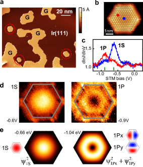
Fig. 1(a) shows a large-scale overview scan of a typical sample. We find interconnected graphene patches (indicated by G) as well as small isolated GQDs (red dotted circles). The CVD growth yields a relatively broad distribution of different GQD sizes ranging from a couple of nanometers up to ca. 20 nm, most of them with a roughly hexagonal shape. All the GQDs have edges in the zigzag direction (corresponding to the close-packed atomic rows of the underlying Ir(111) surface) with a very small roughness. We see kinks of one or two atomic rows at the GQD edges EPA . Closer inspection of small GQDs at a bias voltage close to zero bias shows that the edges are bright both in the actual STM topography as well as in the simultaneously recorded images. These edge states are expected for zigzag edges in graphene Son et al. (2006); Brey and Fertig (2006); Koskinen et al. (2008); Castro Neto et al. (2009). More information can be found in the Supplementary Information EPA .
We now focus on the delocalized, quantum confined states inside the GQDs. We can map the atomic structure of the GQD by STM as shown for a small GQD with perfect hexagonal symmetry with 7 benzene ring long edges in Fig. 1(b). The LDOS can be accessed through measurements as shown in Fig. 1(c); we clearly observe an increased and spatially dependent LDOS on the GQDs. There is a pronounced maximum of the LDOS measured in the center of the GQD (blue line in Fig. 1(c)) at a bias of -0.6 V. Moving away from the center of the GQD, the intensity of this peak is reduced, and another resonance emerges at a bias of -0.9 V (red line). We can map the spatial shape of the orbitals responsible for these resonances by measuring the signal during STM imaging under constant-current feedback at biases corresponding to the resonances [Fig. 1(d)]. These states have the familiar appearance of the lowest energy levels of the text book particle-in-a-box problem and can be characterized using symmetry labels borrowed from atomic physics. The lowest state has symmetry (no nodal planes) and the first excited state is composed of two type orbitals ( and ) which are degenerate in this case of a perfect hexagonal GQD. STM probes the sum of the squared wavefunctions leading to a doughnut shaped signal as we observe in the experiment. Comparison of these states with TB calculations can be found in the Supplementary Information EPA .
We note here that at positive bias, electronic resonances with clear peaks in the spectrum cannot be observed EPA . Based on DFT calculations on Ir(111), there is a dense set of energy bands above the Fermi energy at the K point of Brillouin zone. It is likely that interaction with these states masks the intrinsic graphene states at positive bias Pletikosić et al. (2010).
These experiments can be reproduced by both TB calculations and by a continuum model for particles with linear dispersion confined to a GQD EPA . Here we use the KG equation Heiskanen et al. (2008); Barbier et al. (2008)
| (1) |
where is the Fermi velocity ( m/s in isolated graphene) and the boundary condition is given by = 0 at the edges of the GQD. A more accurate boundary condition would be needed to take into account the sublattice pseudospin and the interaction with the Ir substrate. It is clear that the KG equation cannot be used to model the edge states (in contrast to the Dirac equation and TB calculations Brey and Fertig (2006); Son et al. (2006); Castro Neto et al. (2009)). However, as shown below, the LDOS plots from the KG equation are remarkably similar to the TB calculations and the experimental results, although the number of states in a given energy interval is too small. We use the experimentally determined geometries of the GQD in our calculations EPA . The lowest energy solutions of Eq. (1) are plotted in Fig. 1(e) as the squared wavefunctions corresponding to the experimentally measured , where is the energy resolution of the experiment Tersoff and Hamann (1985).
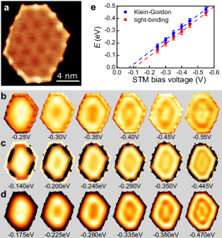
We have measured the LDOS at different bias voltages on a larger GQD shown in Fig. 2(a). The periodic variation with a period of 2.5 nm seen on the topographic STM images is a moiré pattern resulting from the lattice mismatch between graphene and Ir Coraux et al. (2009); Sun et al. (2011). The STM contrast results mostly from a small (ca. 30 pm) geometric modulation of the graphene structure Sun et al. (2011). Our calculations neglecting this moiré-induced potential modulation yield quantitative agreement with the experiment and the expected potential modulation due to the moiré pattern is small compared to the confinement energy in our GQDs. It has been reported that the size and shape of the GQDs is influenced by the moiré pattern and the edges prefer to run along the fcc and hcp regions of the moiré N’Diaye et al. (2008); Coraux et al. (2009). We also observe GQDs that are smaller than the moiré period ( and ). For larger GQDs, the kinks on the edges are spaced by roughly one moiré period.
The asymmetry of the GQD breaks the degeneracies (e.g. and states) of the purely hexagonal GQD. This can be seen in the measured LDOS maps shown in Fig. 2(b) (The Ir substrate has been removed in the images using the simultaneously acquired STM topography image as a mask, images with the background can be found in the Supplementary Information EPA ): after the state (bias -0.25 V), we observe increased intensity at the top and bottom end of the GQD consistent with the envelope wavefunction along the long GQD axis (at -0.30 V). At more negative bias, the state also contributes and the long GQD edges are brighter (-0.35 V). Subsequently, the next eigenstate becomes relevant, which is seen as an increased intensity in the middle of the QD (bias -0.4 V).
In order to compare experiment and theory in detail, we have generated a series of theoretical LDOS maps, which are calculated as a weighted and broadened sum of squares of TB molecular orbitals (MOs) or KG eigenstates close to a given energy [see Figures 2(c,d)] EPA . This broadening is justified due to the intrinsic resolution of the measurement (75meV) and the life-time broadening of the states. In the case of the calculations based on the KG equation,the eigenfunctions are given by the solution of Eq. (1) using the overall shape of the GQD. In the TB calculations (we use third-nearest-neighbor TB) Son et al. (2006); Castro Neto et al. (2009); Hancock et al. (2010), they correspond to the calculated MOs for the GQD with an exact atomic structure as obtained from experiment [Fig. 2(a)] EPA . It can be seen that the eigenstates of the KG equation (overall geometry) match with clusters of TB MOs (exact atomic lattice). Furthermore, there is a remarkable agreement in how both calculated LDOS maps evolve with energy and how the experimental conductance maps evolve with the bias.
Based on a comparison between the experimental and computed LDOS maps, we have identified energy / bias voltage pairs that give the same spatial features in the LDOS with an associated error estimate indicated by error bars in Fig. 2(e) EPA . It is clear that with the Fermi-velocity as the only adjustable parameter (in the case of TB calculations, is directly related to the value of the hopping integrals), both calculations agree strikingly well with the experiments. This is also evident from Fig. 2(e), where we show the correspondence between the experimental bias voltages and the theoretical energies. This gives the Fermi velocity m/s as the best-fit to both the KG equation and the TB calculations. The two theories yield slightly different values for the doping of the GQD, i.e. the intercept of the -axis, due to the differences in the theoretical approaches.
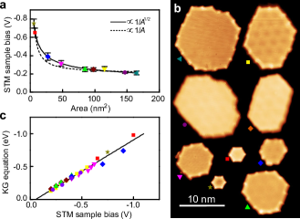
Do we see the peculiar nature of the charge carriers in graphene in these LDOS maps? In fact, the Schrödinger equation predicts wavefunctions with an identical spatial shape as the KG equation since both are second order differential equations; the corresponding eigenenergies are related as . This also explains the different dispersion relations for free electrons, which are either parabolic (Schrödinger) or linear (Klein-Gordon). Moreover, the energy of the lowest (and the other) quantum confined state scales as ( is the area of the QGD) in the case of the relativistic massless particles, instead of for the particles obeying the Schrödinger equation. We demonstrate in Fig. 3 that the charge carriers in our GQDs fulfil the conditions of and have a linear dispersion. Fig. 3(a) shows the bias voltage corresponding to the lowest quantum confined energy level (determined by the peak position in vs. spectra acquired at the center of the GQD) on many different GQDs [topographies shown in Fig. 3(b)] as a function of the experimentally determined area. The solid line showing the expected scaling fits the data clearly better than the (dashed line) behavior.
In Fig. 3(c), we present the correspondence between experimental bias voltages (-axis) and the theoretical energies calculated with the KG equation (-axis) for many states on several GQDs. The one-to-one correspondence confirms that the experimental data is consistent with the linear dispersion of the Klein-Gordon equation. The corresponding Fermi velocity m/s is slightly smaller than the previous results on macroscopic graphene samples on Ir(111) obtained by ARPES ( to m/s) Pletikosić et al. (2009); Rusponi et al. (2010); Starodub et al. (2011). Possible reasons for this discrepancy are that our STM measurements probe the average Fermi velocity around the Dirac cone (in contrast to ARPES) and our experiments are carried out on GQDs instead of bulk graphene. Remarkably, remains constant down to the smallest structures that we have measured. The intercept with the -axis in Fig. 3(c) and the extrapolation to infinite GQD area in Fig. 3(a) indicate that GQDs on Ir(111) are n-doped by 0.1 eV.
In summary, we have presented low-temperature STM and STS experiments aimed at understanding the quantum confined energy levels and their spatially resolved wavefunctions in atomically well-defined graphene quantum dots. The measured resonances and corresponding LDOS maps correspond to a number of molecular orbitals close in energy, calculated by TB for the exact atomic geometry. The energy position and LDOS structure of these clustered states can also be calculated from the relativistic wave-equation for massless particles. Our results provide experimental verification of the physics relevant for graphene-based opto-electronics where wavefunction engineering via well-defined nanostructuring is likely to be a central issue. In addition, our experiments indicate that the intrinsic electronic states of graphene can be studied on weakly interacting metal substrates (e.g. Ir(111)). These systems can act as future test beds for studying the effects of chemical modifications or doping of graphene.
Acknowledgements.
This research was supported by the Academy of Finland (Projects 117178, 136917, and the Centre of Excellence programme 2006-2011), FOM (”Control over Functional Nanoparticle Solids (FNS)”), the Finnish Academy of Science and Letters, and NWO (Chemical Sciences, Vidi-grant 700.56.423).Note added.–During the review of this letter, we became aware of related experiments presented in Refs. Subramaniam et al. (2011); Phark et al. (2011).
References
- Geim and Novoselov (2007) A. K. Geim and K. S. Novoselov, Nature Mater. 6, 183 (2007).
- Castro Neto et al. (2009) A. H. Castro Neto, et al., Rev. Mod. Phys. 81, 109 (2009).
- Li et al. (2009) X. S. Li, et al., Science 324, 1312 (2009).
- Schwierz (2010) F. Schwierz, Nature Nano. 5, 487 (2010).
- Han et al. (2007) M. Y. Han, et al., Phys. Rev. Lett. 98, 206805 (2007).
- Rycerz et al. (2007) A. Rycerz, J. Tworzydlo, and C. W. J. Beenakker, Nature Phys. 3, 172 (2007).
- Ponomarenko et al. (2008) L. A. Ponomarenko, et al., Science 320, 356 (2008).
- Jiao et al. (2009) L. Jiao, et al., Nature 458, 877 (2009).
- Kosynkin et al. (2009) D. V. Kosynkin, et al., Nature 458, 872 (2009).
- Ritter and Lyding (2009) K. A. Ritter and J. W. Lyding, Nature Mater. 8, 235 (2009).
- Cai et al. (2010) J. Cai, et al., Nature 466, 470 (2010).
- Sprinkle et al. (2010) M. Sprinkle, et al., Nature Nano. 5, 727 (2010).
- Rutter et al. (2007) G. M. Rutter, et al., Science 317, 219 (2007).
- Sun et al. (2011) Z. Sun, et al., and P. Liljeroth, Phys. Rev. B 83, 081415(R) (2011).
- Martin et al. (2008) J. Martin, et al., Nature Phys. 4, 144 (2008).
- Zhang et al. (2008) Y. B. Zhang, et al., Nature Phys. 4, 627 (2008).
- Deshpande et al. (2009) A. Deshpande, et al., Phys. Rev. B 79, 205411 (2009).
- Zhang et al. (2009) Y. Zhang, et al., Nature Phys. 5, 722 (2009).
- Wang et al. (2011) B. Wang, et al., Nano Lett. 11, 424 (2011).
- Eom et al. (2009) D. Eom, et al., Nano Lett. 9, 2844 (2009).
- Coraux et al. (2009) J. Coraux, et al., New J. Phys. 11, 023006 (2009).
- Morgenstern (2003) M. Morgenstern, Surf. Rev. Lett. 10, 933 (2003).
- (23) See EPAPS Document No. XXX for additional results and experimental details.
- Son et al. (2006) Y.-W. Son, M. L. Cohen, and S. G. Louie, Phys. Rev. Lett. 97, 216803 (2006).
- Brey and Fertig (2006) L. Brey and H. A. Fertig, Phys. Rev. B 73, 235411 (2006).
- Koskinen et al. (2008) P. Koskinen, S. Malola, and H. Häkkinen, Phys. Rev. Lett. 101, 115502 (2008).
- Pletikosić et al. (2010) I. Pletikosić, et al., J. Phys.: Condens. Matter 22, 135006 (2010).
- Heiskanen et al. (2008) H. P. Heiskanen, M. Manninen, and J. Akola, New J. Phys. 10, 103015 (2008).
- Barbier et al. (2008) M. Barbier, et al., Phys. Rev. B 77, 115446 (2008).
- Tersoff and Hamann (1985) J. Tersoff and D. R. Hamann, Phys. Rev. B 31, 805 (1985).
- N’Diaye et al. (2008) A. T. N’Diaye, et al., New J. Phys. 10, 043033 (2008).
- Hancock et al. (2010) Y. Hancock, et al., Phys. Rev. B 81, 245402 (2010).
- Pletikosić et al. (2009) I. Pletikosić, et al., Phys. Rev. Lett. 102, 056808 (2009).
- Rusponi et al. (2010) S. Rusponi, et al., Phys. Rev. Lett. 105, 246803 (2010).
- Starodub et al. (2011) E. Starodub, et al., Phys. Rev. B 83, 125428 (2011).
- Subramaniam et al. (2011) D. Subramaniam, et al., arXiv:1104.3875.
- Phark et al. (2011) S. Phark, et al., ACS Nano, DOI: 10.1021/nn2028105.