High-resolution spatial mapping of the temperature distribution of a Joule self-heated graphene nanoribbon
Abstract
We investigate the temperature distributions of Joule self-heated graphene nanoribbons (GNRs) with a spatial resolution finer than 100 nm by scanning thermal microscopy (SThM). The SThM probe is calibrated using the Raman G mode Stokes/anti-Stokes intensity ratio as a function of electric power applied to the GNR devices. From a spatial map of the temperature distribution, heat dissipation and transport pathways are investigated. By combining SThM and scanning gate microscopy data from a defected GNR, we observe hot spot formation at well-defined, localized sites.
Energy dissipation and heat flow in nanostructured graphene devices are critical issues for understanding charge transport mechanisms and for further optimization of device performance. Local temperature distributions of Joule self-heated graphene devices have been studied by optical methods such as micro-Raman spectroscopy, micro-infra-red and confocal Raman spectroscopy Freitag09 ; donghunNL10 ; marcus10 ; mhbae10 ; Balandin08 . The spatial resolution of these optical techniques, however, is limited by the photon wavelength 1 m, and a new type of the thermal probe is required to investigate microscopic energy dissipation mechanism in graphene nanostructures whose dimensions are often much smaller than this length scale. While scanning thermal microscopy(SThM) Majumdar93 ; Leinhos98 ; Mills98 ; Shi01 has been used for studying thermal dissipation of nanoscaled devices ShiJAP09 ; Pkim02 ; Insun11 with a spatial resolution of 50 nm, due to the complex heat transfer paths involved, this technique requires a non-trivial calibration process for the thermal probe in order to correctly represent the local sample temperature on an absolute scale ShiPhD .
In this letter, we present a high-resolution study of the spatial distribution of the temperature of graphene nanoribbons (GNRs) under conditions of current flow. The measurements were carried out using SThM, with an absolute calibration of the temperature rise by means of Raman spectroscopy. In this fashion, we were able to probe the thermal contact resistance between a GNR and the underlying substrate.
The fabrication process for the GNR devices used in these experiments has been described in previous work HanPRL07 . Briefly, single layer graphene samples were deposited by mechanical exfoliation on Si wafers covered with 280 nm thick SiO2. Cr/Au electrodes (0.5 nm/40 nm in thickness) were defined by electron beam lithography. A negative tone e-beam resist, hydrogen silsesquioxane (HSQ), was used to form an etch mask for an oxygen plasma etching process which removed the unprotected graphene.

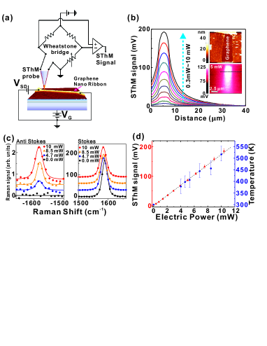
Fig. 1(a) shows a schematic diagram for SThM measurements of the Joule self-heated GNR devices. The SThM experiments were carried out with an atomic force microscope (AFM) probe with a high-resolution thermistor installed at the tip (XE-100 with Nano thermal probe, Park Systems Corp.). The measurements were performed in a dry nitrogen environment at room temperature. The resistance change of the thin palladium film resistor at the apex of the probe is monitored using a Wheatstone bridge. The SThM signal is obtained from the off-balance bridge signal, which is proportional to the local temperature change of the thermal probe. In order to calibrate this SThM signal on an absolute temperatures scale, we employ Raman spectroscopy. For this purpose, we use a standard wide-channel graphene device (Fig. 1(b)) with a channel area of 4 10 m2 to create a relatively uniform temperature distribution by Joule heating under electrical bias. The SThM signal is recorded at a fixed power (i.e., fixed bias voltage ), as shown in Fig. 1. Then we employ micro-Raman spectroscopy with 1 m probing beam spot (Fig. 1(c)) to measure the absolute temperature of the same standard graphene device. The temperature of the G-mode phonons () can be obtained from the ratio of the anti-Stokes and Stokes signals through the relation to , where is the G-phonon energy (195 meV), is the Boltzmann constant and is a previously determined numerical factor that depends on the Raman susceptibilities of the Stokes and anti-Stokes processes as well as the spectral response of our experimental arrangement stephanePRL . In the low power limit studied here, non-equilibrium effects can be neglected and is assumed to be equal to the sample temperature . As seen in Fig. 1(d), both the off-balance bridge SThM signal, , and the measured from Raman spectroscopy depend linearly on the applied electric power . From these data we obtain the conversion factor between the and the temperature increase : [mV] K, where is room temperature. This conversion factor varies 25 among the different SThM probes used in this study.

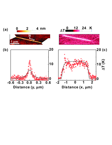
Exploiting these calibrated SThM probes, we acquired an AFM topography image (Fig. 2(a), left) and an SThM image (Fig. 2(a), right) of a GNR with a channel width nm and a length 3 m that was connected to wide graphene source and drain electrodes. The SThM image shows a spatial map of for the device with an applied voltage of 3 V, resulting in a total Joule heating of 78 W. Heat generation and dissipation pathways in the GNR can be investigated by taking cross-sections of the SThM temperature distribution. Below we consider two particular directions: along the GNR ( direction) and perpendicular to the GNR ( direction), where the origin of coordinate system is located at the center of the GNR. Fig. 2(b) shows at the center of the GNR. decreases rapidly near the GNR, then slowly approaches at large . Since the GNR has a large ratio, we employ a 2-dimensional (2D) heat diffusion equation to describe the steady-state temperature profile in the oxide layer below the GNR, with denoting the direction into the substrate:. We solve this equation with mixed boundary conditions: , , and , where 280 nm is the thickness of SiO2. Here the three boundary conditions correspond, respectively, to the assumptions that complete thermal equilibration occurs at Si/SiO2 interface, that no heat flows across the SiO2/air interface, and that the substrate temperature right beneath of the GNR is given by a constant value Ts. The latter assumption is justified because the width w of the nanoribbon is much less than the oxide thickness . We use the finite element method with as a single fitting parameter to match the experimental temperature profile. The dashed line in Fig. 2(b) shows the best fit obtained for +6.2 K. From this model calculation, the corresponding total heat flux to the substrate for the 3 m long GNR is estimated to be 60 W, assuming the thermal conductivity of SiO2 is 1.5 W/mK. Comparing this value to 78 W, the total electrical power is dissipated in the GNR, we see that 75 % of the heat generated in the GNR dissipates through the substrate, and the remaining heat is presumably removed by dissipation through the GNR channel to the electrodes. We note that is substantially lower than the peak value 12.3 K measured at . This means that there is a finite contact thermal resistance leading to a temperature difference between the GNR and the underlying SiO2 substrate. From the total heat flow through this contact corresponding to , we obtain 2.710-8 m2 K/W, in reasonable agreement with other larger scale graphene devices studied previously Freitag09 ; Chen09 ; YongECS10 ; popJAP07 ; MakAPL10 .
We now discuss the longitudinal temperature profile along the GNR (Fig. 2(c)). is nearly constant away from the source () and the drain () regions, consistent with the above conclusion that most of the heat generated by Joule heating is not transported through the GNR. Utilizing the fact that the GNR has a large aspect ratio and that heat dissipation is generated by the applied electric power density , we apply the 1-dimensional (1D) heat diffusion equation to model the longitudinal temperature profile along the GNR: with the boundary condition , where is the thermal conductance of the GNR and 410-8 m2 K/W is the effective thermal contact resistance estimated from . The solution of this differential equation is given by , where is the characteristic length scale of the temperature changes near the junction area. Fitting this equation to the measured temperature profile along the -direction (dashed line in Fig. 2(c)), we obtain =0.23 m. Considering and above are upper bounds due to the simple model we use in this work, we estimate an upper bound of the thermal conductance of the GNR as 1.32 W/K, corresponding to an upper bound of thermal conductivity 3800 W/mK, where the effective thickness of the graphene layer has been take as the van der Waals value of 0.34. This result is in reasonable agrement with the reported graphene thermal conductivity of graphene Balandin08 ; Freitag09 .

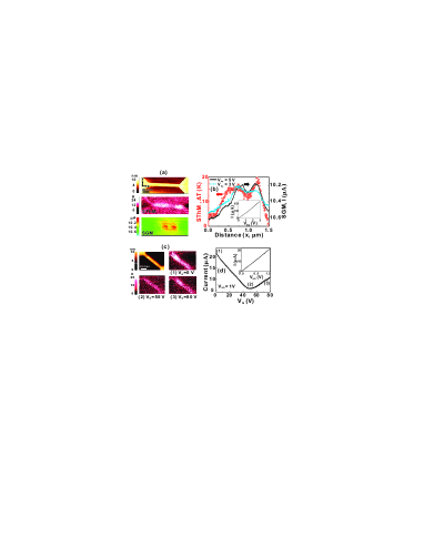
The high spatial resolution of our SThM also allows us to investigate the heat dissipation mechanism associated with any localized defects in a GNR. Although no such defects were present in the GNR studied above, in Fig. 3(a) we show topographic, SThM, and scanning gate microscopy (SGM) Bachtold00 images of a defective GNR. Here we use a Cr/Au metal coated AFM probe to apply a gate voltage at a constant height of 30 nm. As shown in Fig. 3(a), the topographic AFM image of the GNR exhibits no appreciable structural defects within the spatial resolution limit 30 nm. However, as seen in the SGM image, this particular GNR has two local defect sites where the current can be suppressed by 5% by the SGM tip. The SThM image taken under the same conditions reveals that these local areas indeed correspond to local heat sources, appearing in the SThM image (Fig. 3(a)) as two bright spots whose temperature is 30% higher than the neighboring areas. Close inspection of the SGM and SThM signal profiles (Fig. 3(b)) indicates that they are well correlated and the spatial resolution of the SThM is as high as 100 nm. Further investigation of the localized heat dissipation effect can be performed by inspecting the gate-dependent SThM images as shown in Fig. 3(c) and (d). The role of such localized heat dissipation by defects is strongly influenced by the gating conditions of the device. The ability of SThM to probe this effect is illustrated in Figs. 3(c) and (d), in which the temperature profile of another defected GNR device is probed as a function of the applied gating voltage.
This work is supported by the ONR graphene MURI, FENA FCRP, DARPA CERA and NRF(National Honor Scientist Program: 2010-0020414, WCU: R32-2008-000-10180-0) program.
References
- (1) A. A. Balandin, S. Ghosh, W. Bao, I. Calizo, D. Teweldebrhan, F. Miao, and C. N. Lau, Nano. Lett. 8, 902 (2008).
- (2) M. Freitag, M. Steiner, Y. Martin, V. Perebeinos, Z. Chen, J. C. Tsang, and P. Avouris, Nano. Lett. 9, 1883 (2009).
- (3) D.-H. Chae, B. Krauss, K. von Klitzing, and J. H. Smet, Nano. Lett. 10, 466 (2010).
- (4) M. Freitag, H.-Y. Chiu, M. Steiner, V. Perebeinos, and P. Avouris, Nature Nanotech. 5, 497 (2010).
- (5) M.-H. Bae, Z.-Y. Ong, D. Estrada, and E. Pop, Nano. Lett. 10, 4787 (2010).
- (6) A. Majumdar, J. P. Carrejo, and J. Lai, Appl. Phys. Lett. 62, 2501 (1993).
- (7) G. Mills, H. Zhou, A. Midha, L. Donaldson, and J. M. R. Weaver, Appl. Phys. Lett. 72 2900 (1998).
- (8) T. Leinhos, M. Stopka, and E. Oesterschulze, Appl. Phys. A: Mater. Sci. Process. 66, 65 (1998).
- (9) L. Shi, O. Kwon, A. C. Miner, and A. Majumdar, J. Microelectromech. Syst. 10, 370 (2001).
- (10) L. Shi, J. Zhou, P. Kim, A. Bachtold, A. Majumar, and P. L. McEuen, J. Appl. Phys. 105, 104306 (2009).
- (11) P. Kim, L. Shi, A. Majumdar, and P. L. McEuen, Physica. B 323, 67 (2002).
- (12) I. Jo, I.-K. Hsu, Y. J. Lee, M. M. Sadeghi, S. Kim, S. Cronin, E. Tutuc, S. K. Banerjee, Z. Yao, and L. Shi, Nano. Lett. 11, 85 (2011).
- (13) L. Shi, Ph.D. thesis, University of California, Berkeley, 2001
- (14) M. Y. Han, B. zyilmaz, Y. Zhang, and P. Kim, Phys. Rev. Lett. 98, 206805 (2007).
- (15) S. Berciaud, M. Y. Han, K. F. Mak, L. E. Brus, P. Kim, and T. F. Heinz, Phys. Rev. Lett., 104, 227401 (2010).
- (16) Z. Chen, W. Jang, W. Bao, C. N. Lau, and C. Dames, Appl. Phys. Lett. 95, 161910 (2009).
- (17) L. A. Jauregui, Y. Yue, A. N. Sidorov, J. Hu, Q. Yu, G. Lopez, R. Jalilian, D. K. Benjamin, D. A. Delk, W. We, W. Wu, Z. Liu, X. Wang, Z. Jiang, X. Ruan, J. Bao, S. S. Pei, Y. P. Chen, ECS Transactions 28, 73 (2010).
- (18) K. L. Grosse, M.-H. Bae, F. Lian, E. Pop and W. P. King, Nature Nanotechnol. 6, 287 (2011).
- (19) K. F. Mak, C. H. Lui, and T. F. Heinz, Appl. Phys. Lett. 97, 221904 (2010).
- (20) A. Bachtold, M. S. Fuhrer, S. Plyasunov, M. Forero, E. H. Anderson, A. Zettl, and P. L. McEuen, Phys. Rev. Lett. 84, 6082 (2000).