Coupled study by TEM/EELS and STM/STS of electronic properties of C- and CNx-nanotubes
Résumé
Carbon nanotubes are the focus of considerable research efforts due to their fascinating physical properties. They provide an excellent model system for the study of one dimensional materials and molecular electronics. The chirality of nanotubes can lead to very different electronic behaviours, either metallic or semiconducting. Their electronic spectrum consists of a series of Van Hove singularities defining a bandgap for semiconducting tubes and molecular orbitals at the corresponding energies. A promising way to tune the nanotubes electronic properties for future applications is to use doping by heteroatoms. Here we report on experimental investigation of the role of many-body interactions in nanotube bandgaps, the visualization in direct space of the molecular orbitals of nanotubes and the properties of nitrogen doped nanotubes using scanning tunneling microscopy and transmission electron microscopy as well as electron energy loss spectroscopy.
Résumé Etude couplée par TEM/EELS et STM/STS des propriétés structurales et électroniques des nanotubes C et CNx
Les nanotubes de carbone sont l’objet d’importants efforts de recherche en raison de leurs fascinantes propriétés physiques. Ils constituent un système modèle particulièrement intéressant pour l’étude fondamentale de matériaux à une dimension et pour l’électronique moléculaire. En fonction de leur chiralité, les nanotubes peuvent adopter un comportement électronique soit semiconducteur soit métallique. Leur spectre électronique est dominé par une série de singularités de Van Hove qui définit la bande interdite des tubes semiconducteurs et les orbitales moléculaires situées à ces énergies. Pour contrôler et moduler les propriétés électroniques des nanotubes, une voie prometteuse est d’utiliser le dopage par des hétéroatomes. Les travaux présentés ici portent sur l’étude expérimentale de l’influence des interactions à N corps sur la valeur de la bande interdite des tubes semiconducteurs, la visualisation dans l’espace direct des orbitales moléculaires des nanotubes et les propriétés des nanotubes dopés par l’azote en utilisant des mesures de microscopie tunnel, microscopie électronique à balayage et spectroscopie de perte d’énergie des électrons.
keywords:
Carbon nanotubes; STM/STS; EELSMots-clés : Nanotubes de carbone; STM/STS; EELS
1 Introduction
Carbon nanotubes (CNTs) have attracted considerable interest for their unique electronic properties due to their one dimensional character [1, 2]. A nanotube consists in a single graphene layer rolled up into a hollow cylinder. The many possibilities to roll up this sheet lead to different chiralities for the CNTs. Depending on this chirality, the resulting CNTs can be either metallic or semiconducting. This special link between atomic structure and electronic properties makes the CNTs fascinating candidates for molecular electronics. A promising way to further tune and control the electronic structure of CNTs is to dope them with foreign atoms. Direct doping during the synthesis opens a promising route for potential applications, such as field emission, gas sensor and negative differential resistance (NDR) devices [3, 4, 5, 6, 7]. In this context, multiwall nanotubes containing nitrogen dopants (CNx-MWNTs) have been successfully produced by different groups [8, 9]. However, the as-grown CNx-MWNTs usually have a bamboo-like structure involving a high density of defects, which complicates the investigation of nitrogen configurations and nitrogen-induced effects. Compared to MWNTs, single-wall nanotubes (SWNTs) are better candidates, but only a few studies on the synthesis of nitrogen-doped SWNTs (CNx-SWNTs) have been reported [10, 11, 12]. In these studies, chemical characterization, such as electron energy loss spectroscopy (EELS) [10, 12] or X-ray photoelectron spectroscopy (XPS) [11], has been employed to analyze the C-N bonding environment, as done before on CNx materials, films or multi-wall nanotubes [4, 5]. These studies on CNx-SWNTs diverge, to some extent, in their interpretation of C-N bonding. An efficient approach providing more than chemical information is needed to understand nitrogen incorporation and doping impact on the atomic and electronic structure of nanotubes.
Scanning tunneling microscopy (STM) and scanning tunneling spectroscopy (STS) are powerful tools to measure local electronic properties of SWNTs and correlate them with their atomic structure [13, 14]. Theoretical calculations [15, 16, 17] have shown that a single defect (vacancy, pentagon, adatom) can manifest itself as a perturbation in the carbon network in STM images and as a modification of the local density of states (LDOS) in STS measurements. Thus STM/STS measurements can reveal the atomic structure and the DOS change of nanotube-based hetero-junctions [18, 19, 20], plasma-sputtered nanotubes [21] and other nanotube based systems. Czerw et al [22] have reported STM/STS studies on CNx-MWNTs. However, studies concerning CNx-SWNTs are still scarce.
In the case of pristine nanotubes, the pioneering experiments of local tunneling spectroscopy on SWNTs have been interpreted within a tight-binding single particle model [23, 24, 25] neglecting many-body effects. The same model was also able to reproduce optical measurements. However it has been shown that excitons have a major contribution to the optical transitions [26, 27, 28, 29]. As a consequence, the similar values of the gap of SWNTs measured either by STM — not expected to be sensitive to the excitons — or optical absorption became unclear and it is necessary to revisit the STS study of SWNTs.
In this context, we studied by STS the electronic bandgaps of pure C-SWNTs and solved this apparent controversy using a model where many-body effects are screened by the image charge induced in the metallic substrate. In order to provide a complete picture of the electronic structure of nanotubes as can be measured at the atomic scale by STM, we also investigated the wavefunctions associated to the Van Hove singularities (VHSs) which can be regarded as nanotube molecular orbitals. These orbitals play a major role in controlling the electronic bandstructure of carbon nanotubes upon doping or functionalization [30]. The modification of the electronic structure of CNTs by nitrogen doping has also been studied [31] by coupling morphology analysis by TEM, chemical characterization by EELS and STM/STS measurements.
2 Experimental
Different sorts of nanotubes were used in the present study. Using the home-made reactor at ONERA [32], pure carbon SWNTs were synthesized in the arc discharge configuration whereas the nitrogen doped nanotubes were synthesized in the laser vaporization configuration described elsewhere [31]. The synthesis products were ultrasonically dispersed in absolute ethanol for 15 min and deposited on grids for TEM studies (Philips CM20, 200 kV) of the morphology and of the diameter of nanotubes. Several tens of pure carbon nanotubes were statistically analyzed. Using a Gaussian fit, we obtained a statistical distribution of tube diameter centred on 1.4 nm with a full-width at half-maximum of 0.2 nm. A third type of tubes was synthesized in a vertical flow aerosol reactor [33]. EELS experiments have been carried out in a dedicated scanning TEM (STEM) VG-HB501 (100 KV). We used a sligthly defocussed probe of a few nm in diameter, with a convergence angle of 15 mrad and a collection angle of 24 mrad. Particular attention has been devoted to contamination and damage during acquisition. STM measurements at room temperature were performed using an Omicron Nanotechnology © variable temperature STM. STM/STS measurements were performed using an Omicron Nanotechnology © low temperature (5K) STM operating under UHV conditions (less than mbar). Arc and laser nanotubes were deposited from a dispersion in alcohol after sonication onto a single-crystalline Au (111) surface previously cleaned under UHV condition by repeated cycles of ion argon sputtering and annealing at 800 K. The samples were dried in air and introduced into the UHV system. CVD nanotubes were deposited in situ onto commercial gold on glass surface previously flashed by butane flame in air. Before STM/STS measurements, the samples were outgassed for 2 hours to remove residual molecules. All measurements were performed with tungsten tips.
3 Electronic bandgap of CNTs on a Au(111) surface
3.1 Bandgap distribution in a bundle of nanotubes
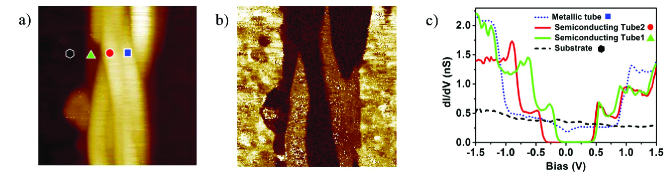
After dispersion and deposition on the Au(111) substrate, most of the nanotubes remain arranged in bundles, allowing us to measure bandgaps of single nanotubes, either directly in contact with the metallic substrate, or separated from the metal by neighboring nanotubes. In Fig. 1(a), we present the topographic image of a bundle on the Au(111) substrate. The nanotubes are intertwined in the bundle. The differential conductance image at 20 mV (Fig. 1(b)) depicting the distribution of the local densities of states permits us to distinguish clearly the metallic from the semiconducting tubes in the bundle. Its color scale corresponds to the level of the LDOS at 20 mV and reveals the presence of semiconducting tubes in the bundle, that appear dark whereas the metallic tubes appear with a color code closer to that of the gold substrate.
This conductance image can be further understood by looking at the dI/dV spectra plotted in Fig. 1(c). On the gold substrate, the differential conductance has a constant non-zero value, as expected (black dashed curve). On the nanotubes, the spectra are dominated by VHSs. On the metallic tube, the conductance (blue dotted spectrum) between the two first singularities is close to that of the substrate, except around the Fermi level where it displays a local minimum. This pseudo-gap [34] can be induced by a curvature effect [35] or to intertube interactions [36]. Two spectra of semi-conducting tubes are also shown in Fig. 1(c). The spectrum of tube 1 (green curve) exhibits a strong asymmetry with respect to the Fermi level, which can be attributed to charge transfer from the substrate [13, 14, 37] . The energy separation between the first two singularities on each side of the Fermi level is denoted E for semiconducting tubes and E for metallic tubes, respectively. One can measure these values at the point of maximum slope in the peak [38] . In this way, is found to be equal to 0.70 eV (green spectrum) for tube 1 directly contacting the substrate and to 0.91 eV for tube 2 (red spectrum) at the top of the bundle.
The renormalization of the electronic gap of a molecule due to substrate-induced charging effects in STS measurement has been already studied both theoretically and experimentally [39, 40, 41]. The screening effect due to the image charge in the metal was found to account for the decrease of the electronic gap of the molecules deposited on the substrate. For the nanotubes, when they are in contact with a metallic substrate, this effect should also be considered. Here the measured value of tube 1 is indeed smaller than for tube 2 and the difference cannot be explained by the distribution in tube diameters [42]. This suggests that the tube-substrate distance would probably have an impact on the value measured by STS.
3.2 Bandgap reduction due to screening by the metallic substrate
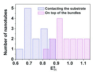
In order to verify the relation between the tube-substrate separation and the measured bandgap, we have also studied the pure carbon SWNTs synthesized by CVD. The histogram of the measured values (see Fig. 2) shows a clear right shift of measured on the top of bundles (red) with respect to those measured on the tubes contacting the substrate (blue), in good agreement with the results obtained on the arc samples.
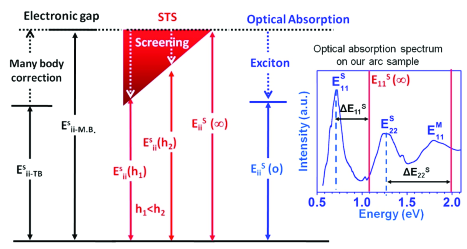
The present observation can be explained as follows (see the scheme in Fig. 3). According to the literature, the intrinsic gap of semiconducting tubes is the sum of the single-particle gap and of the self-energy induced by the many-body effect [43, 44]. In STS measurements, the screening effect can be understood from an image charge model, where the transition of a nanotube adsorbed on a metal corresponds to the gap of the free nanotube (including electron-electron interactions) reduced by the screening energy resulting from the image charge in the metal , where is the tube-substrate distance [42]. For the tubes contacting the substrate (), the many-body effect is practically compensated by the substrate-induced screening, which reduces significantly the gap and approaches the single-particle gap value. As increases (), the screening effect decreases and leads to larger experimental STS values. The limit , allows us then to estimate the unscreened gap of nanotubes.
Experimentally, the major role played by many-body effects has been first demonstrated by optical measurements [43, 44]. The electron-hole interaction confined in the quasi one dimension system leads to important excitonic effect in the optical absorption. At first glance, the STM experiments are not supposed to be sensitive to such an electron-hole interaction [27]. Therefore, it is instructive to compare the STS measurement with optical absorption experiments. The inset in Fig. 3 shows the optical absorption spectrum measured on the same patch of arc nanotubes. The energy difference (E) between the optical transition and the asymptotic values by STS is then expected to correspond to the exciton binding energy. In this way, we obtain 0.4 eV, close to the value determined in previous optical measurements [44].
4 The molecular orbitals of carbon nanotubes
In the context of controlling the electronic band structure of carbon nanotubes using doping or functionalization, the molecular orbitals of SWNTs play a major role, since they are fully involved in the transport properties and the chemical reactivity of SWNTs [30]. It has been predicted that, in defect-free semiconducting tubes, the electronic states would exhibit broken symmetry [45, 46, 16, 47]. Local conductance measurement of SWNTs using atomically resolved STS allows us to investigate such an asymmetry at VHSs.
4.1 Semiconducting tube: 3p+1
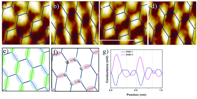
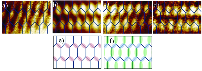
In Fig. 4(a-d), we present the differential conductance images (dI/dV maps) in color scale of a semiconducting tube at the energies of the VHSs. The hexagonal lattice is determined on the topographic image [48] and superimposed in the images to indicate the position of carbon atoms. The significant deformation of the lattice is mostly due to the drift occurring during the long acquisition time as well as distorsions induced by the curvature of the nanotube. These conductance images show a strong anisotropy of density of states which is energy-dependent. More precisely, for the images at VHS+1 and VHS-2, one third of the C-C bonds are highlighted while the other C-C bonds are more intense at VHS-1 and VHS+2. The four images can be summarized into two different patterns sketched in Fig. 4(e,f). The superimposition of these two types of images, such as VHS1, restitutes a full sixfold symmetry. In Fig. 4(g), we plot the differential conductance profiles along an hexagon. Starting from the atom labeled 1 in Fig. 4(f), the VHS+1 profile in the clockwise direction of the hexagon displays two maxima corresponding to higher DOS and four minima indicating lower DOS. The maxima/minima of VHS+1 are exactly at the same position as the minima/maxima of VHS-1. The conductance profile at VHS-1 has the mirror symmetry with respect to the profile at VHS+1, demonstrating clearly the complementary nature of these two patterns.
4.2 Semiconducting tube: 3p-1
Similar patterns with broken symmetry were systematically observed on the defect-free nanotubes. Fig. 5 shows the dI/dV maps of a second type of semiconducting tube. At VHS+1 and VHS-2, two thirds of the C-C bonds have a maximum of LDOS. The most inclined bond with respect to the axial orientation has maxima of electron density at VHS-1 and VHS+2, presenting an opposite behavior to that of the previous example. As will be shown in the following, this behavior is the signature of (n,m) tubes with wheras the example shown in the previous section is typical of a tube.
4.3 Tight binding analysis
In the literature, interference patterns have been observed in STM topographic images close to defects such as chemical impurities, cap ends or in finite length nanotubes [49, 50, 51]. Differential conductance images have also been obtained in a finite length tube using local differential conductance spectroscopy [52]. These observations have been explained qualitatively by interference effects between the Bloch waves [45, 53, 50]. In contrast, our results of dI/dV maps were performed far from the extremity of the tube and were observed systematically. Our observations are consistent with the prediction that the electronic states would display broken symmetry effect [46, 49, 45, 47, 54].
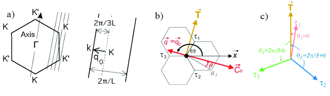
A chemist approach in real space [48] appears to be very fruitful also as we show now. We follow the classical zone-folding theory based on a tight binding description of the graphene band structure. The rolling up of the graphene sheet implies that the allowed vectors belong to the so-called cutting lines parallel to the tube axis, separated by , where is the length of the chiral vector and is the diameter of the tube. If (n,m) are the coordinates of the chiral vector, the position of the cutting lines with respect to the points depends on the value of modulo 3. In the case of metallic tubes, and some cutting lines are going through the points. In the case of semiconducting tubes, , and the nearest line is at a distance on the left (resp. right) hand side of point when (resp. ). This depends on the specific choice of the point (see Fig. 6(a)), but the final result of our analysis will not. Close to the point, the linearity of the dispersion relation of graphene implies that the energy is proportional to . For a tube, as indicated in Fig. 6(a), the vector of its LUMO state corresponds to , where , is defined as a vector of length pointing along the direction of the chiral vector in the negative direction. On the other side of the point, the vector corresponds to the second singularity. The Bloch eigenstates of a singularity have only a double trivial degeneracy , being close to a point of the Brillouin zone.
Since there are two atoms per unit cell in the graphene structure, the eigenstates are built from two independent Bloch states and :
| (1) |
These two Bloch states are linear combinations of atomic state at site in the two sublattices.
| (2) |
Dropping for simplicity the indices, the wavefunctions in real space can be written as:
| (3) |
where is the atomic orbital centered on site . 111Here we consider only the states. We can now calculate the electronic density ,
| (4) |
This development involves an expansion in products of the atomic wavefunctions at different sites. For :
| (5) |
In the first neighbor approximation, the overlap function can be neglected when , because first neighbour sites belong to different sublattices and the above terms reduce to the superposition of atomic densities:
| (6) |
In the same approximation, the cross term is given by:
| (7) |
where and are first neighbors. Close to the point, the ratio is given by: 222In the tight binding model, the Hamiltonian has only off-diagonal non-vanishing matrix elements: and . The eigenvalues of energy is given by , where is thet transfer integral between first neighbors. , and are the vectors joining one atom to its three first neighbors, as indicated in Fig. 6. Close to a point, and . Thus, by developing ito first order in , , where is the C-C nearest neighbor distance, is the module of , is the angle between and the axis, see Fig. 6(a). The energy depends only on the modulus of . Since , , the ratio is then directly obtained.
| (8) |
where sgn()= 1 depends on the sign of and is the angle between and the axis. This implies that the ratio just introduces a phase factor related to the direction of the vector, i.e. finally to the chiral angle , as indicated in Fig. 6(b). The chiral angle here is precisely defined as the smallest angle between the lattice vector and the chiral vector , so that . Since we can normalize the density in Eq. (4) by fixing these quantities equal to unity. Finally, combining Equations. (6), (7) and (4), we obtain the expression of the local density of states , which is the quantity measured in STS. can be written as:
| (9) | |||||
where is the density of states, is the superposition of electron atomic densities and is the interference centered on the C-C bonds.
The breaking of the sixfold symmetry is caused by the second term . Its intensity is proportional to the nearest neighbor overlap. Then, is one of the vectors between first neighbors shown in Fig. 6(b,c). Keeping only the terms of lowest order, we can also replace by , and the interference term can be written as:
| (10) |
where .
From Eq. (10), we see that the electronic density of the interference term is determined by the factor . To discuss the value of , let us first consider the LUMO state of a tube. As mentioned above, the corresponding vector , points along the negative direction of the chiral vector , so that (see Fig. 6(b)). When , , , is equal to , 0 and respectively and the corresponding values of are equal to , and . As shown in Fig. 6(c), these angles are equal to the angles between the tube axis and the C-C bonds . We have . Switching to the LUMO+1 case, the vector should take the value . This leads to a shift of in with respect to the LUMO state and inverts the sign of . Considering both the sign of and , there are four possibilities, as listed in table. 1. Depending on the sign of , basically two types of images are then expected:
| HOMO-1 | HOMO | LUMO | LUMO+1 | |
| - | - | + | + | |
| - | + | + | - | |
| + | - | - | + | |
| + | - | - | + | |
| + | - | + | - | |
| - | + | - | + | |
| - | + | - | + | |
| Image Type | I | II | I | II |
Image of Type I: . As schematically illustrated in Fig. 4(e), the electron density above the C-C bonds pointing close to the tube axis () is reinforced, all the more when is small, i.e. close to a zig-zag orientation ().
Image of Type II: . In this case, when the chiral angle is close to zig-zag orientation , the images present stripe reinforcements on the bonds perpendicular to the axis (), as indicated in Fig. 4(f). The images of type I and type II are complementary and the superposition of both types reconstitutes the six-fold symmetry of the graphene network. As increases, and the density on the corresponding bonds ( in Fig. 6(b,c)) gradually vanishes and the density concentrates principally on the bonds .
To summarize, for the tubes such that , the LUMO and HUMO contributions are of type I and type II, respectively, presenting complementary natures, because the corresponding values are opposite. When going from the first VHS to the neighboring second VHS (same sign of ), the vectors are along opposite directions, implying a shift of in the phase factor , which inverts the sign of . Therefore, the singular contribution at the second VHSs is also complementary of those of the first ones.
Considering now the other family of semiconducting tubes, where , the vector of the LUMO state should be replaced by , giving rise to a phase shift of with respect to the tubes. Thus, the LUMO state presents the image type II. By analogy with the analysis in table. 1, their HOMO-1, HOMO, LUMO and LUMO+1 states correspond to the images of type II, I, II and I, respectively, and are complementary to those of the tubes. These results agree perfectly with those obtained by Kane and Mele [45].
Turning back to experimental data, in Fig. 4(a-d) (see section 4.1), we have observed exactly only two types of interference images as predicted by the tight-binding model. The axially oriented C-C bond has maximum electron density at VHS+1 and minimum density at VHS-1. This implies that the investigated tube belongs to the family . As for the tube shown in Fig. 5 (see section 4.2), its conductance images at VHS-1 and VHS+1 exhibit the interference pattern of Type I and Type II, respectively. According to our tight binding model, it belongs to the family .
5 Nitrogen doped single-walled carbon nanotubes
After having attained a deep understanding of the electronic properties of pure carbon nanotubes, we now study nitrogen incorporation and its doping impact on the atomic and electronic structure of nanotubes.
5.1 Structural and chemical characterization of CNx-SNWTs by TEM/EELS
Fig. 7(a) displays a TEM image of as-grown products dispersed in solution. We observe a random network of single-walled nanotubes, which are assembled into bundles. These bundles contain a number of tubes varying from a few units to a few tens. The tubes are well-crystallized, and very few defects are observed.
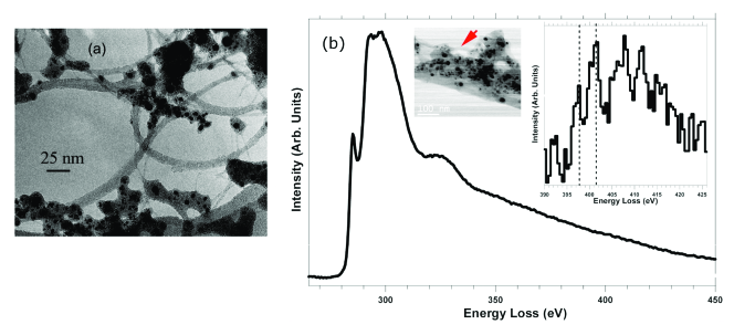
Local chemical characterization of as-grown nanotubes has been previously carried out using spatially-resolved electron energy loss spectroscopy (SREELS) of bundles of SWNTs and individual nanotubes [12]. This analysis revealed a mean nitrogen content about 1.7 atom . Fig. 7(b) shows a representative example of the EELS spectrum recorded of those NTs. This EELS spectrum corresponds to the sum of six EEL spectra acquired on the bundle of NTs shown in the bright field image (acquisition conditions are described elsewhere [12]; the acquisition time was two seconds for each spectrum). From the shape of the C-K edge it can be deduced that the nanotubes consist of a typical graphitic network with sp2-type bonding and that the tubes are very well graphitized [6, 12]. The inset of Fig. 7(b) shows the N-K edge. Two features can be observed at 398 and 402 eV, respectively. They could be attributed to the states of the pyridine-like and graphitic-like configuration, respectively [6, 12]. As a matter of fact, we observed a predominance of pyridine-like nitrogen configuration [12].
5.2 Structural and electronic characterization of CNx-SNWTs by STM/STS
Following this chemical analysis, STM measurements of CNx-SWNTs have revealed the presence of defects with different characteristics. Fig. 8(a) displays a tube containing multiple defects. Two types of perturbation of carbon network, appearing as a local protrusion, can be readily distinguished. The rectangle indicates the first defect with large spatial extension (56 nm), comprising axially oriented spots with a 0.44 nm periodicity, as indicated by the black dots in the magnified image of Fig. 8(b). Similar defect has been previously observed in our CNx-SWNTs and reported in [31]. We will present later on a detailed study on this kind of defect by combining STS spectroscopic data.
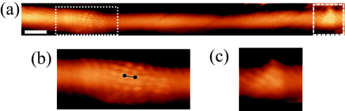
The second defect is indicated by the square in Fig. 8(a) and a magnified image in Fig. 8(c). It appears as a local protrusion with a series of “ridges” aligned along its axial direction. Compared to the first defect, its spatial extension is much smaller, 1 nm. It is worth mentioning that such a signature has also been observed several times in our CNx-SWNTs. Even if the exact configuration of this defect is not known, we can exclude some cases. We first consider topological defects. The signature of a vacancy is predicted to be a bright hillock structure [15, 55] and it has few in common with the present observation. The present signature is more similar to the presence of a pentagon in the graphitic network which is a ring protrusion [46] or a Stone-Wales defect exhibiting a combination of double rings protrusion with ridge-like structure [16]. According to DFT calculations [56], the signature of a single graphitic nitrogen is a triangular bright spot cluster weakly sensitive to STM bias, which seems to exclude the possibility of a single nitrogen atom in a substitutional site. The observation of two different defect signatures in the same tube also indicates that these two signatures should correspond to different atomic structures.
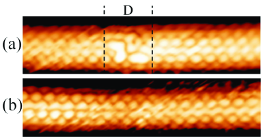
Fig. 9(a) shows the image of a nanotube measured at 1.0 V. The defect is localized in the middle of the image (zone D). The difference in height between the defect and the other part of the tube is very small, which is different from the local protrusions presented above. It is worth noting that, next to the defect site, the STM image exhibits an interference pattern over long distance with a periodicity ( is the graphene lattice constant). This pattern can be interpreted in terms of electronic interference originating from large momentum scattering of the electron wave functions at the defect site between two nonequivalent K points, which leads to a modulation in the electron density [45, 49]. Similar patterns have been experimentally obtained in the vicinity of tube end caps [50], of defects created by hydrogen electron [57] and STM tip-induced defects [58]. In an oversimplified description, such an interference pattern is a fingerprint of the presence of a localized defect, which can act as an electron scatterer. In our observation, since the amplitude of the DOS oscillation decreases with the distance, the mixture of various electron states leads to a continuous change in the imaging pattern [50]. Upon increasing the bias voltage up to 1.3 V, the perturbation area (zone D) fades out, and the tube presents a uniform interference pattern over a distance of 10 nm, consisting of bright spots and wavy lines. Such long range interference patterns have been frequently observed, suggesting the existence of a several localized defects in our CNx-SWNTs.
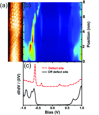
In order to have a deeper understanding of the defects observed in our CNx-SWNTs, a spectroscopic study has been undertaken at low temperature. Fig. 10(a) displays an atomically resolved STM image of a nanotube with a protrusion with a spatial extension about 6 nm, similar to the first defect reported above. In Fig. 10(b), we plot the color map of differential conductance spectra as a function of the bias voltage and the position along the tube, which is oriented vertically. Starting from the defect-free zone at the bottom of the image, the tube exhibits a typical electronic structure of a defect-free semiconducting tube. In Fig. 10(c), a typical STS of this defect-free zone (black curve) exhibits the two first VHSs, giving an electronic gap about 1.2 V. When the tip approaches the protrusion zone, two new states appear inside the electronic gap at around -0.37 V and 0.24 V, respectively (dashed curve in Fig. 10(c)). Referring to the literature, paired states near the Fermi level have been attributed to the presence of vacancy-adatom complex [59] or any two close point defects [57]. Assuming that this defect is due to the presence of nitrogen, there are several possibilities based on the understanding of paired states : 1) the presence of several nitrogen atoms; 2) the combination of nitrogen with vacancy. This observation is in line with the results presented above where the defects observed cannot be explained by a simple substitution of a nitrogen atom in the carbon lattice, but most likely by a complex structure.
5.3 Nitrogen configuration in CNx-SWNTs
The C-N bonding in nitrogen doped CNTs has been studied in previous works by Glerup et al. [10] and Ayala et al. [60] who found that the nitrogen is incorporated in the walls with both graphitic and pyridine-like forms. In contrast to these analysis, our EELS results suggest that the pyridine-like configuration is preferentially stabilized in SWNT, with respect to the graphitic one [12]. Some recent theoretical studies concerning the formation energy of pyridinic and graphitic configurations have proved the possibility of having only pyridinic configurations under some conditions: on the basis of first-principles total energy calculations, Min et al. [61] showed that the pyridine-like nitrogen configuration is indeed energetically favored as compared to graphitic configuration when two hydrogen atoms are attached to passivate the broken carbon bond. Yang et al. [62] showed that pyridine-like nitrogen becomes more favorable than graphite-like nitrogen as the diameter decreases and as the chiral angle increases, in agreement with [63]. It is also worth noting that Ayala et al. [60] have reported that pyridine-like configuration occurs at higher synthesis temperature while the graphitic substitution configuration fades away. At the highest temperature achieved in their synthesis (950∘), they showed a predominance of pyridine-like configuration. These results support our EELS findings.
Turning back to STM data, the protrusion with small extension observed in our CNx-SWNTs cannot be due to the presence of a single graphitic nitrogen, whose signature is predicted to be a triangular bright cluster. In addition, if the large protrusion in our sample observed by STM/STS is indeed caused by nitrogen, its electronic structure is also consistent with a non-graphitic nitrogen configuration. It is generally believed that the graphitic nitrogen gives rise to a donor state [64, 65], while we observed a double peak structure within the gap. All these results imply that the graphitic nitrogen is not the dominant one in our CNx-SWNTs, which is in line with EELS analysis [12]. Therefore, although a chemical characterization cannot be unambiguously performed from the STM/STS data, we can conclude that, if nitrogen atoms are at the origin of the defects observed, the dominant configuration is probably not a single simple substitution.
In order to have a general idea of defect distribution and defect content in our CNx-SWNTs, we have performed a statistical study of the atomically resolved STM images. Defects have been detected in 1/3 of the investigated zones (each is 20 nm). Assuming that all the defects observed by STM measurements are due to the presence of nitrogen, the frequency of their detection in STM images is at first sight hardly compatible with the N concentration determined from EELS, which revealed an average nitrogen concentration of 1.7 at [12]. If the distribution of nitrogen atoms on the tube surface is homogenous, according to EELS data, we should be able to observe a defect associated with the presence of nitrogen every 4 nm (this estimation takes into account the fact that N atoms can be randomly distributed along the tube circumference and that only the upper side of tube can be detected by the STM tip). This apparent discrepancy between EELS and STM data can be explained by a heterogenous N distribution, in which case we should find some areas rich in N atoms. This leads to the question of the nature of N configurations when embedded in the graphitic network. As discussed above, nitrogen atoms are incorporated in SWNTs as complex defects, involving several nitrogen atoms. Thus, a smaller frequency of defect detection can be expected, as it is the case of our STM measurement. This also agrees with the inhomogeneous distribution of nitrogen at the surface of tubes found in the EELS analysis. Indeed, as shown in Fig. 8, we observe a long range unperturbed zone ( 20 nm), but highly perturbed zones in some areas of the tubes.
Summarizing our results, STM data reveal the presence of different defects in our CNx-SWNTs. These defects could be most likely made of complex structures involving one or more nitrogen and defects such as vacancies or 5/7 rings. STM and EELS results indicate that the nitrogen atoms are not regularly dispersed along the tubes. Based on this understanding, we would expect that the structure of nitrogen rich defects might vary from one defect to another, randomly dispersed along the tube.
6 Conclusion
In this study, we have discussed the structural and electronic properties of pristine and CNx single-walled nanotubes by combining TEM/EELS and STM/STS analyses. Firstly, we have evidenced the role of many-body effects played in STS and the role of the metal substrate which screens these interactions via the image charge. The comparison between STS and optical absorption measurement has allowed us to estimate the exciton binding energy of the semiconducting tubes. Secondly, we have performed a complete experimental investigation of the molecular orbitals associated with Van Hove singularities in pure semiconducting SWNTs. Using a simple tight-binding model, we have analyzed the symmetry of wavefunctions in SNWTs and demonstrated that the molecular orbitals of nanotubes at the Van Hove singularities display only complementary behaviours. Finally, based on the analysis by TEM/EELS and STM/STS, we have tentatively proposed a model for our CNx-SWNTs: the insertion of nitrogen atoms should be associated with different structural defects, such as vacancies or pentagons and/or heptagons and the clusters of these structures disperse randomly along the tubes.
7 Acknowledgments
This study has been supported by the European Contract STREP “BCN” Nanotubes 30007654-OTP25763, by a grant of CNano IdF “SAMBA” and by the ANR project “CEDONA” of the PNANO programme (ANR-07-NANO-007_02). We gratefully acknowledge Luc Henrard, Patrick Hermet and Bin Zheng for fruitful discussions.
References
- [1] R. Saito and G. Dresselhaus, Physical Properties of Carbon Nanotubes, Imperial College Press, 1998.
- [2] A. Loiseau, P. Launois, P. Petit, S. Roche, and J. Salvetat, Understanding carbon nanotubes, Springer, 2006.
- [3] M. Terrones, A. Jorio, M. Endo, A. Rao, Y. Kim, T. Hayashi, H. Terrones, J.-C. Charlier, G. Dresselhaus, and M. Dresselhaus, New direction in nanotube science, Materials Today 7 (2004) 30.
- [4] C. P. Ewels and M. Glerup, Nitrogen Doping in Carbon Nanotubes, Journal of Nanoscience and Nanotechnology 5 (2005) 1345.
- [5] P. Ayala, R. Arenal, A. Loiseau, A. Rubio, and T. Pichler, The physical and chemical properties of heteronanotubes, Rev. Mod. Phys. 82 (2010) 1843.
- [6] P. Ayala, R. Arenal, M. Rümmell, A. Rubio, and T. Pichler, The doping of carbon nanotubes with nitrogen and their potential applications, Carbon 48 (2010) 575.
- [7] R. Arenal, X. Blase, and A. Loiseau, Boron-nitride and boron-carbonitride nanotubes: synthesis, characterization and theory, Advances in Physics 59 (2010) 101.
- [8] M. Terrones, P. Ajayan, F. Banhart, X. Blase, D. Carroll, J. Charlier, R. Czerw, B. Foley, N. Grobert, R. Kamalakaran, P. Kohler-Redlich, M. Rühle, T. Seeger, and H. Terrones, N-doping and coalescence of carbon nanotubes: synthesis and electronic properties, Applied Physics A: Materials Science & Processing 74 (2002) 355.
- [9] M. Glerup, H. Kanzow, R. Almairac, M. Castignolles, and P. Bernier, Synthesis of multi-walled carbon nanotubes and nano-fibres using the aerosol method with metal-ions as the catalyst precursors, Chemical Physics Letters 377 (2003) 293.
- [10] M. Glerup, J. Steinmetz, D. Samaille, O. Stephan, S. Enouz, A. Loiseau, S. Roth, and P. Bernier, Synthesis of N-doped SWNT using the arc-discharge procedure, Chemical Physics Letters 387 (2004) 193.
- [11] P. Ayala, A. Gruneis, C. Kramberger, M. H. Rummeli, I. G. Solorzano, F. L. Freire, and T. Pichler, Effects of the reaction atmosphere composition on the synthesis of single and multiwalled nitrogen-doped nanotubes., J. Chem. Phys. 127 (2007) 184709.
- [12] H. Lin, R. Arenal, S. Enouz-Vedrenne, O. Stephan, and A. Loiseau, Nitrogen Configuration in Individual CNx-SWNTs Synthesized by Laser Vaporization Technique, The Journal of Physical Chemistry C 113 (2009) 9509.
- [13] J. W. G. Wilder, L. C. Venema, A. G. Rinzler, R. E. Smalley, and C. Dekker, Electronic structure of atomically resolved carbon nanotubes, Nature 391 (1998) 59.
- [14] T. W. Odom, J.-L. Huang, P. Kim, and C. M. Lieber, Atomic structure and electronic properties of single-walled carbon nanotubes, Nature 391 (1998) 62.
- [15] A. V. Krasheninnikov, Theoretical STM Images of Carbon Nanotubes with Atomic Vacancies: A Systematic Tight-Binding Study, Phys. Low-Dim. Struct 11/12 (2000) 1.
- [16] V. Meunier and P. Lambin, Scanning tunneling microscopy and spectroscopy of topological defects in carbon nanotubes, Carbon 38 (2000) 1729.
- [17] D. Orlikowski, M. Buongiorno Nardelli, J. Bernholc, and C. Roland, Theoretical STM signatures and transport properties of native defects in carbon nanotubes, Phys. Rev. B 61 (2000) 14194.
- [18] M. Ouyang, J.-L. Huang, C. L. Cheung, and C. M. Lieber, Atomically Resolved Single-Walled Carbon Nanotube Intramolecular Junctions, Science 291 (2001) 97.
- [19] H. Kim, J. Lee, S.-J. Kahng, Y.-W. Son, S. B. Lee, C.-K. Lee, J. Ihm, and Y. Kuk, Direct Observation of Localized Defect States in Semiconductor Nanotube Junctions, Phys. Rev. Lett. 90 (2003) 216107.
- [20] M. Ishigami, H. J. Choi, S. Aloni, S. G. Louie, M. L. Cohen, and A. Zettl, Identifying Defects in Nanoscale Materials, Phys. Rev. Lett. 93 (2004) 196803.
- [21] G. Buchs, P. Ruffieux, P. Groning, and O. Groning, Scanning tunneling microscopy investigations of hydrogen plasma-induced electron scattering centers on single-walled carbon nanotubes, Appl. Phys. Lett. 90 (2007) 013104.
- [22] R. Czerw, M. Terrones, J. C. Charlier, X. Blase, B. Foley, R. Kamalakaran, N. Grobert, H. Terrones, D. Tekleab, P. M. Ajayan, W. Blau, M. Rühle, and D. L. Carroll, Identification of electron donor states in N-doped carbon nanotubes, Nano Letters 1 (2001) 457.
- [23] N. Hamada, S.-i. Sawada, and A. Oshiyama, New one-dimensional conductors: Graphitic microtubules, Phys. Rev. Lett. 68 (1992) 1579.
- [24] J. W. Mintmire, B. I. Dunlap, and C. T. White, Are fullerene tubules metallic?, Phys. Rev. Lett. 68 (1992) 631.
- [25] R. Saito, M. Fujita, G. Dresselhaus, and M. S. Dresselhaus, Electronic structure of graphene tubules based on C60, Phys. Rev. B 46 (1992) 1804.
- [26] T. Ando, Excitons in Carbon Nanotubes, Journal of the Physical Society of Japan 66 (1997) 1066.
- [27] C. L. Kane and E. J. Mele, Ratio Problem in Single Carbon Nanotube Fluorescence Spectroscopy, Phys. Rev. Lett. 90 (2003) 207401.
- [28] M. S. Dresselhaus, G. Dresselhaus, R. Saito, and A. Jorio, Exciton Photophysics of Carbon Nanotubes, Annual Review of Physical Chemistry 58 (2007) 719.
- [29] T. Ando and U. Seiji, Theory of Electronic States in Carbon Nanotubes, Phys. Stat. Sol. (c) 6 (2009) 173.
- [30] M. S. Strano, C. A. Dyke, M. L. Usrey, P. W. Barone, M. J. Allen, H. Shan, C. Kittrell, R. H. Hauge, J. M. Tour, and R. E. Smalley, Electronic Structure Control of Single-Walled Carbon Nanotube Functionalization, Science 301 (2003) 1519.
- [31] H. Lin, J. Lagoute, C. Chacon, R. Arenal, O. St?han, V. Repain, Y. Girard, S. Enouz, L. Bresson, S. Rousset, and A. Loiseau, Combined STM/STS, TEM/EELS investigation of CNx-SWNTs, Phys. Stat. Sol. (b) 245 (2008) 1986.
- [32] J.-L. Cochon, J. Gavillet, M. L. de la Chapelle, A. Loiseau, M. Ory, and D. Pigache, A continuous wave CO2 laser reactor for nanotubes synthesis, in AIP Conf. Proc., volume 486, AIP, Kirchberg, Tirol (Austria), 1999, pp. 237–240.
- [33] T. Susi, A. G. Nasibulin, P. Ayala, Y. Tian, Z. Zhu, H. Jiang, C. Roquelet, D. Garrot, J.-S. Lauret, and E. I. Kauppinen, High quality SWCNT synthesis in the presence of NH3 using a vertical flow aerosol reactor, phys. stat. sol. (b) 246 (2009) 2507.
- [34] M. Ouyang, J.-L. Huang, C. L. Cheung, and C. M. Lieber, Energy Gaps in “Metallic” Single-Walled Carbon Nanotubes, Science 292 (2001) 702.
- [35] A. Kleiner and S. Eggert, Curvature, hybridization, and STM images of carbon nanotubes, Phys. Rev. B 64 (2001) 113402.
- [36] P. Delaney, H. Joon Choi, J. Ihm, S. G. Louie, and M. L. Cohen, Broken symmetry and pseudogaps in ropes of carbon nanotubes, Phys. Rev. B 60 (1999) 7899.
- [37] L. C. Venema, V. Meunier, P. Lambin, and C. Dekker, Atomic structure of carbon nanotubes from scanning tunneling microscopy, Phys. Rev. B 61 (2000) 2991.
- [38] L. C. Venema, J. W. Janssen, M. R. Buitelaar, J. W. G. Wild er, S. G. Lemay, L. P. Kouwenhoven, and C. Dekker, Spatially resolved scanning tunneling spectroscopy on single-walled carbon nanotubes, Phys. Rev. B 62 (2000) 5238.
- [39] R. Hesper, L. H. Tjeng, and G. A. Sawatzky, Strongly reduced band gap in a correlated insulator in close proximity to a metal, EPL (Europhysics Letters) 40 (1997) 177.
- [40] X. Lu, M. Grobis, K. H. Khoo, S. G. Louie, and M. F. Crommie, Charge transfer and screening in individual C60 molecules on metal substrates: A scanning tunneling spectroscopy and theoretical study, Phys. Rev. B 70 (2004) 115418.
- [41] J. D. Sau, J. B. Neaton, H. J. Choi, S. G. Louie, and M. L. Cohen, Electronic Energy Levels of Weakly Coupled Nanostructures: C[sub 60]-Metal Interfaces, Phys. Rev. Lett. 101 (2008) 026804.
- [42] H. Lin, J. Lagoute, V. Repain, C. Chacon, Y. Girard, J.-S. Lauret, F. Ducastelle, A. Loiseau, and S. Rousset, Many-body effects in electronic bandgaps of carbon nanotubes measured by scanning tunnelling spectroscopy, Nat. Mater. 9 (2010) 235.
- [43] F. Wang, G. Dukovic, L. E. Brus, and T. F. Heinz, The Optical Resonances in Carbon Nanotubes Arise from Excitons, Science 308 (2005) 838.
- [44] G. Dukovic, F. Wang, D. Song, M. Y. Sfeir, T. F. Heinz, and L. E. Brus, Structural Dependence of Excitonic Optical Transitions and Band-Gap Energies in Carbon Nanotubes, Nano Letters 5 (2005) 2314.
- [45] C. L. Kane and E. J. Mele, Broken symmetries in scanning tunneling images of carbon nanotubes, Phys. Rev. B 59 (1999) R12759.
- [46] V. Meunier and P. Lambin, Tight-Binding Computation of the STM Image of Carbon Nanotubes, Phys. Rev. Lett. 81 (1998) 5588.
- [47] P. Lambin, G. I. M rk, V. Meunier, and L. P. Bir , Computation of STM images of carbon nanotubes, International Journal of Quantum Chemistry 95 (2003) 493.
- [48] H. Lin, J. Lagoute, V. Repain, C. Chacon, Y. Girard, F. Ducastelle, H. Amara, A. Loiseau, P. Hermet, L. Henrard, and S. Rousset, Imaging the symmetry breaking of molecular orbitals in single-wall carbon nanotubes, Phys. Rev. B 81 (2010) 235412.
- [49] W. Clauss, D. J. Bergeron, M. Freitag, C. L. Kane, E. J. Mele, and A. T. Johnson, Electron backscattering on single-wall carbon nanotubes observed by scanning tunneling microscopy, EPL (Europhysics Letters) 47 (1999) 601.
- [50] M. Furuhashi and T. Komeda, Chiral Vector Determination of Carbon Nanotubes by Observation of Interference Patterns Near the End Cap, Phys. Rev. Lett. 101 (2008) 185503.
- [51] L. C. Venema, J. W. Wildöer, J. W. Janssen, S. J. Tans, H. L. Tuinstra, L. P. Kouwenhoven, and C. Dekker, Imaging Electron Wave Functions of Quantized Energy Levels in Carbon Nanotubes, Science 283 (1999) 52.
- [52] S. G. Lemay, J. W. Janssen, M. van den Hout, M. Mooij, M. J. Bronikowski, P. A. Willis, R. E. Smalley, L. P. Kouwenhoven, and C. Dekker, Two-dimensional imaging of electronic wavefunctions in carbon nanotubes, Nature 412 (2001) 617.
- [53] A. Rubio, D. S nchez-Portal, E. Artacho, P. Ordej n, and J. M. Soler, Electronic States in a Finite Carbon Nanotube: A One-Dimensional Quantum Box, Phys. Rev. Lett. 82 (1999) 3520.
- [54] V. Meunier and P. Lambin, Scanning tunnelling microscopy of carbon nanotubes, Philosophical Transactions Of The Royal Society Of London Series A-Mathematical Physical And Engineering Sciences 362 (2004) 2187.
- [55] A. V. Krasheninnikov, Predicted scanning tunneling microscopy images of carbon nanotubes with atomic vacancies, Solid State Communications 118 (2001) 361.
- [56] B. Zheng, P. Hermet, and L. Henrard, personal communication, 2010.
- [57] G. Buchs, A. V. Krasheninnikov, P. Ruffieux, P. Groning, A. S. Foster, R. M. Nieminen, and O. Groning, Creation of paired electron states in the gap of semiconducting carbon nanotubes by correlated hydrogen adsorption, New Journal of Physics 9 (2007) 275.
- [58] M. Berthe, S. Yoshida, Y. Ebine, K. Kanazawa, A. Okada, A. Taninaka, O. Takeuchi, N. Fukui, H. Shinohara, S. Suzuki, K. Sumitomo, Y. Kobayashi, B. Grandidier, D. Stievenard, and H. Shigekawa, Reversible Defect Engineering of Single-Walled Carbon Nanotubes Using Scanning Tunneling Microscopy, Nano Letters 7 (2007) 3623.
- [59] G. Kim, B. W. Jeong, and J. Ihm, Deep levels in the band gap of the carbon nanotube with vacancy-related defects, Appl. Phys. Lett. 88 (2006) 193107.
- [60] P. Ayala, A. Grueneis, T. Gemming, D. Grimm, C. Kramberger, M. H. Ruemmeli, F. L. Freire, H. Kuzmany, R. Pfeiffer, A. Barreiro, B. Buechner, and T. Pichler, Tailoring N-doped single and double wall carbon nanotubes from a nondiluted carbon/nitrogen feedstock, Journal of Physical Chemistry C 111 (2007) 2879.
- [61] Y.-S. Min, E. J. Bae, U. J. Kim, E. H. Lee, N. Park, C. S. Hwang, and W. Park, Unusual transport characteristics of nitrogen-doped single-walled carbon nanotubes, Appl. Phys. Lett. 93 (2008) 043113.
- [62] S. H. Yang, W. H. Shin, and J. K. Kang, The Nature of Graphite- and Pyridinelike Nitrogen Configurations in Carbon Nitride Nanotubes: Dependence on Diameter and Helicity, Small 4 (2008) 437.
- [63] Y. F. Li, Z. Zhou, and L. B. Wang, CN[sub x] nanotubes with pyridinelike structures: p-type semiconductors and Li storage materials, J. Chem. Phys. 129 (2008) 104703.
- [64] A. H. Nevidomskyy, G. Cs nyi, and M. C. Payne, Chemically Active Substitutional Nitrogen Impurity in Carbon Nanotubes, Phys. Rev. Lett. 91 (2003) 105502.
- [65] H. J. Choi, J. Ihm, S. G. Louie, and M. L. Cohen, Defects, Quasibound States, and Quantum Conductance in Metallic Carbon Nanotubes, Phys. Rev. Lett. 84 (2000) 2917.