First-principles study of the spin-mixing conductance in Pt/Ni81Fe19 junctions
Abstract
Based on the spin-pumping theory and first-principles calculations, the spin-mixing conductance (SMC) is theoretically studied for Pt/Permalloy (Ni81Fe19, Py) junctions. We evaluate the SMC for ideally clean Pt/Py junctions and examine the effects of interface randomness. We find that the SMC is generally enhanced in the presence of interface roughness as compared to the ideally clean junctions. Our estimated SMC is in good quantitative agreement with the recent experiment for Pt/Py junctions. We propose possible routes to increase the SMC in Pt/Py junctions by depositing a foreign magnetic metal layer in Pt, offering guidelines for designing the future spintronic devices.
Spintronics utilizes the electron spin degree of freedom for device applications such as data storage, non-evaporate memory, and high speed processing, which exceed the conventional electronics. zutic@rmp04 These spintronic devices are controlled by spin current, and thus efficiently creating the spin current is one of the primary issues. maekawa
One of the standard ways to generate the spin current is the spin-pumping through a ferromagnetic metal/normal metal (F/N) junction where the spin current is pumped out from the F into the N by ferromagnetic resonance in the F. tserkovnyak@prl02 The spin current induced by the spin-pumping is proportional to the spin-mixing conductance (SMC), tserkovnyak@prl02 ; zwierzycki@prb05 ; kardasz@prb10 and thus the large SMC is required for highly efficient F/N junctions as a spin current generator.
The large SMC is also related to the enhanced Gilbert magnetic damping in the F. kardasz@prb10 ; ghosh@apl11 For instance, the critical current density of the current induced magnetization reversal is proportional to the Gilbert damping constant, and the large Gilbert damping is suitable for fast switching of magnetization reversal. sun Thus, the SMC is also an essential parameter to design high speed and low power consumption spintronic devices. In spite of its importance, the SMC is usually employed as a fitting parameter of experimental results. ando Therefore, it is highly desirable to quantitatively evaluate the SMC based on first-principles calculations. zwierzycki@prb05 ; carva@prb07
In this Letter, based on the spin-pumping theory tserkovnyak@prl02 and first-principles calculations, we investigate the SMC in Pt/Permalloy (Ni81Fe19, Py) junctions. We numerically evaluate the SMC for the ideally clean junctions with three different crystalline orientations, and discuss quantitatively the effects of interface randomness. We find that the interface roughness generally enhances the SMC as compared to the ideally clean junctions. Our estimated SMC is found to be in good agreement with the recent experiment. ando We also discuss possible routes to increase the SMC in Pt/Py based junctions by depositing an additional buffer layer in Pt or Py. Our results indicate that a key ingredient to increase the SMC is to deposit in Pt a magnetic layer such as a Fe layer.
Here, the SMC is evaluated based on the spin-pumping theory and using first-principles calculations. In the spin-pumping theory, tserkovnyak@prl02 the SMC is given by , where is the contact area, and denote scattered electronic states at the Fermi energy of the nonmagnetic Pt lead, and is the reflection matrix at the interface for up (down) electrons. note1 Taking into account the realistic electronic structures in the Pt/Py junctions by first-principles calculations, the reflection coefficients are estimated.
We first perform a self-consistent tight-binding linearized muffin-tin orbital (TB-LMTO) calculation andersen@prb86 with atomic sphere approximation for a system consisting of semi-infinite Pt and Py leads, and a scattering region (S) which includes eight layers of Pt and Py for the clean interface, note5 as schematically shown in Fig. 1 (a). Hereafter this system is denoted by PtSPy for short, and thus the ideally clean junction is PtPt(8)Py(8)Py with the number in parentheses indicating the number of atomic layers. The charge and spin densities of Py are treated using virtual crystal approximation (VCA). vca-cpa We use spdf muffin-tin orbital basis set to solve the Schrdinger equation. The exchange-correlation potential is parameterized according to von Barth and Hedin. barth@jpc72 The experimental lattice constant (a=3.55Å) of Py with f.c.c. structure lattice is chosen for both Pt and Py leads for simplicity. mismatch Once the atomic potential in the S is determined self-consistently, the transmission matrix is calculated using a TB-MTO implementation of the wave function matching scheme and the conductance is evaluated using Landauer-Büttiker formula. xia This method has been successfully applied for a number of spin transport calculations including the spin dependent interface resistances and the thermal spin transfer torque in magnetoelectronic devices. xia ; hatami
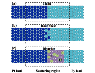
To study the effects of interface randomness, we also consider randomly rough interface. The interface roughness is treated by substituting a composite Pt1-xPyx and PtxPy1-x layer for the first Pt and Py layer at the interface, respectively, as illustrated in Fig. 1 (b). note2 Thus, the S is described by Pt(7)[Pt1-xPyx](1)[PtxPy1-x](1)Py(7). The atomic potential in the S is calculated using the coherent potential approximation (CPA). vca-cpa The concentration is varied from 0 to 0.5 with corresponding to the clean interface. For each , we generate at least 16 different random configurations of atomic positions in the interfacially rough layers, and the SMC is estimated by averaging the results for each random configuration. In addition, to validate the VCA treatment for Py, we study the disordered alloy effects of Py by explicitly including disordered Ni and Fe atomic positions with Ni81Fe19 ratio in the S [Fig. 1 (c)], where Ni and Fe in the S are treated by CPA.
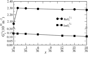
Let us first study -dependence on the SMC in the Pt/Py junctions with crystalline orientation. The obtained results are shown in Fig. 2. It is found that i) the imaginary part of the SMC is approximately one order of magnitude smaller than the real part of the SMC, and ii) the real part of the SMC is larger for the rough interfaces (finite ) than for the clean interface (). Moreover, we can see in Fig. 2 that the SMC is rather insensitive to as long as is finite, and thus we choose for the Pt/Py junctions with the interface roughness studied below.
The results for the SMC with other crystalline orientations, including the one shown above, are summarized in Table 1. We can see in the table that the imaginary part of the SMC (Im ) is about 7 % or less smaller than the real part (Re ), which is similar to the previous studies on different F/N junctions. xia It is also noticed that Re is close to the Sharvin conductance of Pt (). zwierzycki@prb05 Moreover, we find that Re is generally larger for the junctions with the interface roughness than for the ideally clean interface, indicating that the interface roughness plays an important role to achieve a large SMC. Our estimated SMC is in good quantitative agreement with the recent experiment for Pt/Py junctions where the SMC is observed to be about . ando Finally, in Table 1, also shown is the SMC for the disordered Py alloy [Fig. 1 (c)], where we find that the SMC is almost the same for the clean junction illustrated in Fig. 1 (a), justifying VCA for Py alloy.
| Orientation | Interface | ||
|---|---|---|---|
| clean | 2.174 | 0.123 | |
| roughness | 2.347 | 0.185 | |
| clean | 2.354 | 0.128 | |
| roughness | 2.387 | 0.114 | |
| clean | 2.066 | 0.141 | |
| roughness | 2.273 | 0.106 | |
| disorder | 1.996 | 0.055 |
Let us now discuss how to increase the SMC in the Pt/Py based junctions. The SMC is essentially determined by the interface property since this quantity depends on the reflection coefficient at the interface. Therefore, we expect its value to vary by controlling the interface structure. A possible way to obtain a larger SMC is to deposit a buffer layer such as a transition metal (nonmagnetic atomic) layer for a Pt (Py) layer, as schematically shown in Fig. 3. We consider seven different buffer layers and the results are listed in Table 2. We find that the SMC generally increases when a ferromagnetic layer such as Py and Fe, whose magnetic moment is also shown in Table 2, is deposited in the Pt layers. Especially, becomes largest () when two layers of Fe are deposited. Instead, remains almost the same when nonmagnetic metal such as Pt is deposited in the Py layers. Moreover, we can model a tunneling junction by depositing an insulating layer (I) in the Py layers, note4 and the results are also shown in Table 2. It is interesting to notice that the SMC in the tunnel junction remain large () even though the conductance is vanishingly small. A general tendency that we find empirically through this study is that the SMC increases when a magnetic layer is deposited in the nonmagnetic Pt layers in the vicinity of the interface, which we believe can provide guidelines for designing the future spintronic devices.

| PtSPy | ||||
|---|---|---|---|---|
| PtPt(8)Py(8)Py | 2.066 | 0.141 | 2.634 | |
| PtPy(1)Pt(7)Py(8)Py | 2.215 | 0.261 | 2.382 | 0.81 |
| PtFe(1)Pt(7)Py(8)Py | 2.230 | 0.374 | 1.861 | 2.09 |
| PtFe(2)Pt(6)Py(8)Py | 2.520 | 0.228 | 1.859 | 2.03 |
| PtNi(1)Pt(7)Py(8)Py | 1.900 | 0.074 | 2.442 | 0.01 |
| PtPt(8)Py(7)Pt(1)Py | 2.068 | 0.122 | 2.471 | 0.19 |
| PtPy(1)Pt(7)Py(7)Pt(1)Py | 2.179 | 0.301 | 2.212 | 0.9,0.2 |
| PtPt(8)Py(7)I(1)Py | 2.356 | 0.187 | 0.343 | 0 |
In summary, we have studied the SMC in the Pt/Py junctions taking into account the realistic electronic structures by using first-principles calculations. We have evaluated the SMC for the ideally clean junctions and examined the influences of the interface roughness. We have found that the imaginary part of the SMC is approximately one order of magnitude smaller that the real part of the SMC, and that, as compared to the ideally clean junctions, the interface roughness generally enhances the real part of the SMC. We have furthermore discussed possible routes to increase the SMC in Pt/Py based junctions by depositing additional buffer layers in Pt or Py layers. Our results indicate that the SMC increases when a magnetic layer is deposited in the nonmagnetic Pt layers. These results offer valuable guidelines for designing the future spintronic devices.
The authors thank S. Maekawa and J. Ieda for variable comments. A part of the calculation has been performed using RIKEN Integrated Cluster of Clusters (RICC).
References
- (1) I. Zutic, J. Fabian, and S. Das Sarma, Rev. Mod. Phys. 76, 323 (2004).
- (2) S. Maekawa, Concepts in Spin Electronics (Oxford University Press, Oxford, 2006).
- (3) Y. Tserkovnyak, A. Brataas, and G. E. W. Bauer, Phys. Rev. Lett. 88, 117601 (2002).
- (4) M. Zwierzycki, Y. Tserkovnyak, P. J. Kelly, A. Brataas, and G. E. W. Bauer, Phys. Rev. B 71, 064420 (2005).
- (5) B. Kardaz and B. Heinrich, Phys. Rev. B 81, 094409 (2010).
- (6) A. Ghosh, JF Sierra, S. Auffret, U. Ebels, and W. E. Bailey, Appl. Phys. Lett. 98, 052508 (2011).
- (7) J. Z. Sun, Phys. Rev. B 62, 570 (2000).
- (8) K. Ando, Y. Kajiwara, S. Takahashi, S. Maekawa, K. Takemoto, M. Takatsu, and E. Saitoh, Phys. Rev. B 78, 014413 (2008).
- (9) K. Carva and I. Turek, Phys. Rev. B 76, 104409 (2007).
- (10) The general form of the SMC contains and , where and is the transmission matrix for up (down) electrons. However, in metallic junctions, sharply decreases to zero with the thickness of magnetic layers, zwierzycki@prb05 and thus can be safely neglected for thicker junctions.
- (11) O. K. Andersen, Z. Pawlowska, and O. Jepsen, Phys. Rev. B 34, 5253 (1986).
- (12) We set eight layers of Pt and Py in the S to ensure that the electronic structures away from the interface are similar to the bulk.
- (13) I. Turek, V. Drchal, J. Kudrnovský, M. Šob, and P. Weinberger, Electronic Structure of Disordered Alloys, Surfaces and Interfaces (Kluwer, Boston, 1997).
- (14) U. von Barth and L. Hedin, J. Phys. C 5, 1629 (1972).
- (15) B. Glaubitz, S. Buschhorn, F. Brüssing, R. Abrudan and H. Zabel, J. Phys.: Condens. Matter 23, 254210 (2011).
- (16) We have checked the effect of the lattice constant mismatch for Pt and Py by using the lateral supercell sizes of Pt () and Py (), and found that the real part of SMC generally decreases at most about 10 %. However, the main conclusions in this paper are unaffected.
- (17) K. Xia, P. J. Kelly, G. E. W. Bauer, I. Turek, J. Kudrnovsky, and V. Drchal, Phys. Rev. B 63, 064407 (2001); K. Xia, M. Zwierzycki, M. Talanana, P. J. Kelly, and G. E. W. Bauer, Phys. Rev. B 73, 064420 (2006).
- (18) M. Hatami, G. E. W. Bauer, Q. Zhang, and P. J. Kelly, Phys. Rev. Lett. 99, 066603 (2007); M. Hatami, G. E. W. Bauer, Q. Zhang, and P. J. Kelly, Phys. Rev. B 79, 174426 (2009).
- (19) We have checked the lateral supercell size () dependence of the SMC up to , and found that the SMC is already converged for . Therefore, we have adopted for calculations of the SMC presented here.
- (20) A vacuum barrier is adopted as an insulating buffer layer where we use empty spheres to populate the vaccine sites.