First order 0/ quantum phase transition in the Kondo regime of a superconducting carbon nanotube quantum dot
Abstract
We study a carbon nanotube quantum dot embedded into a SQUID loop in order to investigate the competition of strong electron correlations with proximity effect. Depending whether local pairing or local magnetism prevails, a superconducting quantum dot will respectively exhibit positive or negative supercurrent, referred to as a 0 or Josephson junction. In the regime of strong Coulomb blockade, the 0 to transition is typically controlled by a change in the discrete charge state of the dot, from even to odd. In contrast, at larger tunneling amplitude the Kondo effect develops for an odd charge (magnetic) dot in the normal state, and quenches magnetism. In this situation, we find that a first order 0 to quantum phase transition can be triggered at fixed valence when superconductivity is brought in, due to the competition of the superconducting gap and the Kondo temperature. The SQUID geometry together with the tunability of our device allows the exploration of the associated phase diagram predicted by recent theories. We also report on the observation of anharmonic behavior of the current-phase relation in the transition regime, that we associate with the two different accessible superconducting states. Our results ultimately reveal the spin singlet nature of the Kondo ground state, which is the key process in allowing the stability of the 0-phase far from the mixed valence regime.
pacs:
72.15.Qm,73.21.-b,73.63.Fg,74.50+rI Introduction
Realizing a Josephson junction with a carbon nanotube as a weak link opened up the way to a new class of nanoelectronic devices combining both quantum confinement at the nanoscale and the Josephson effect franceschi_2010 ; winkelmann_2009 ; hofstetter_2009 ; herrmann_2009 ; kasumov_1999 ; buitelaar_2002 ; jarillo-herrero_2006 ; dam_2006 ; cleuziou_2006 ; jorgensen_2007 ; cleuziouCM_2006 ; cleuziou_2007 ; pallecchi_2008 ; rasmussen_2009 ; eichler_2009 ; kanai_2010 . In these junctions the critical current could be first thought to be maximized when a discrete electronic level of the quantum dot comes into resonance with the Cooper pair condensate of the electrodes, thus allowing an electrostatic tuning of the magnitude of the critical current beenakker1992 . The Josephson effect in quantum dots is however more complex, because it is governed by the interplay of electronic pairing and strong Coulomb interaction on the dot rozhkov1999 ; clerk2000 ; yoshioka_2000 ; vecino_2003 ; siano_2004 ; choi_2004 ; sellier_2005 ; novotny_2005 ; bauer_2007 ; karrasch_2008 ; meng_2009 . When superconductivity dominates, the superconductor wave function spreads over the dot, inducing a BCS-singlet ground state, i.e. a standard Josephson junction (dubbed the -state in what follows) beenakker1992 . In the other extreme regime of large electron-electron interactions, the quantum dot enters the Coulomb blockade domain, and its charge is locked to integer values, altering the superconducting state. For an odd occupancy, quantum dots behave like a spin magnetic impurity that competes with Cooper pair formation, and the ground state can become a magnetic doublet. In this situation, dissipationless current mainly transits through a fourth order tunneling process reordering the spins of Cooper pairs, thus leading to a negative sign of the supercurrent, which is referred to as the -type Josephson junction glazman_1989 ; dam_2006 ; cleuziou_2006 . These two antagonist superconducting states, associated with a sharp sign reversal of the dissipationless current at zero temperature, can hence allow a first order quantum phase transition by tuning the microscopic parameters in the quantum dot. In the case of very strong Coulomb blockade, the 0- transition is achieved by modifying the parity of the electronic charge on the dot (valence is easily changed using electrostatic gates), so that the supercurrent sign reversal occurs at the edges of the Coulomb diamonds. A more intriguing regime occurs for intermediate Coulomb repulsion (associated to moderately small values of the tunneling amplitude compared to the charging energy), in which Kondo correlations take place: in the normal state, the magnetic impurity of the odd charge state is screened through spin-flip cotunneling processes kouwenhoven_2001 , providing a non-zero density of states at Fermi energy. This so-called Kondo resonance allows the Cooper pairs to flow normally in the superconducting state, and a type Josephson junction is therefore recovered clerk2000 ; choi_2004 ; sellier_2005 ; eichler_2009 ; kanai_2010 . Here we explore in detail how superconducting transport is affected by the presence of Kondo behavior and we finely tune the 0- quantum phase transition in this more complex regime by controlling the quantum dot microscopic parameters.
II Characterization of the nanoSQUID
II.1 Sample fabrication
Here we investigate supercurrent reversal in a carbon nanotube Josephson junction using the nano-SQUID geometry, which implements two Josephson junctions in parallel built with a unique carbon nanotube cleuziou_2006 . The single-wall carbon nanotubes were obtained using laser ablation and then dispersed in a pure dichloroethane solution using low power ultrasounds. A degenerately doped silicon wafer with a 450nm layer of SiO2 on top was used as backgate. A first optical lithography step provided alignment marks in order to locate the nanotubes by scanning electron microscopy. The superconducting loops and the sidegates were fabricated using aligned e-beam lithography, followed by e-beam evaporation of Pd/Al bilayer (with respective thickness 4nm/50nm). All measurements were performed in a dilution refrigerator with a base temperature of mK, and the filtering stages were similar to the ones performed in Ref. cleuziou_2006, . Samples were current-biased, either for DC or lock-in measurements (with an AC amplitude of 10pA), in order to measure directly the switching current or the differential resistance of the device. The nano-SQUID switching currents were detected via a digital filter which monitors the estimated variance of the average DC voltage, see Appendix C and Ref. liu_1995, .
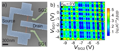
Fig. 1a shows a SEM micrograph of the measured nanotube SQUID with two nm long nanotube Josephson junctions (JJ1 and JJ2). Using the second quantum dot as a (possibly tunable) reference junction, a precise control over the energy and linewidth of the first quantum dot is accessible by tuning a pair of local sidegates and a backgate (, , respectively), see discussion below. Such a geometry allows us to directly measure the Josephson current of a single junction via the magnetic field modulation of the SQUID switching current , see Ref. cleuziou_2006, . Indeed, the critical current of an asymmetric SQUID with sinusoidal current-phase relation (taken here for simplicity) can be written as:
| (1) |
where is the flux modulation of the SQUID, is the magnetic flux quantum, are the intrinsic phase shifts (0 or ) of the two Josephson junctions, and their respective critical currents. The critical current modulation is thus shifted by between the and the SQUID configuration.
II.2 Normal state transport properties
Fig. 1b presents the nano-SQUID stability diagram
at zero bias vs and in the normal state
(a perpendicular magnetic field of mT is applied to suppress superconductivity), at a
given backgate V. This diagram
resembles a weakly tilted checkerboard pattern, which is typical for two parallel
uncoupled quantum dots in the Coulomb blockade regime, with a weak crosstalk of about 4%.
The line-cut at fixed V emphasizes the regions of high and
low differential conductance associated with the Kondo ridges and Coulomb
blockaded valleys respectively. One can indeed distinguish easily between even and odd
occupancies in each dot from the sequence of conducting and blocked regions:
dark blue pockets denote regimes where both dots are blocked (in an even-even
configuration of the double dot setup), green lines correspond to the situation of
a single dot in the Kondo regime (see arrows) while the other remains blocked
(in an even-odd configuration), and red spots show the case where both dots undergo the Kondo
effect (in an odd-odd configuration) kouwenhoven_2001 ; cleuziou_2006 .
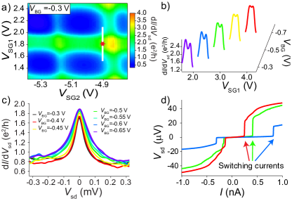
An operating region at a different backgate voltage V is shown with greater detail on Fig. 2a. For between V and V, JJ1 has an odd occupancy associated with a differential conductance close to due to a well-developed Kondo effect. Furthermore, JJ2 clearly has an even number of electrons for between V and V, because of its small contribution to transport in this range. In order to show the influence of the backgate voltage , we have plotted on Fig. 2b the differential conductance vs for the odd occupancy region of JJ1 corresponding to the white cut on Fig. 2a, taking five different values of from V to V. By applying , the sidegates experience a capacitive crosstalk of % and % for sidegate 1 and sidegate 2 respectively, as seen by the global shifts of the conductance traces. The application of a backgate voltage thus modifies the occupation number on the dot, but also the tunnel linewidth grabert_1992 ; cleuziouCM_2006 . Indeed, by varying the backgate voltage and correcting the sidegates voltages for crosstalk, it is possible to keep the local Coulomb repulsion and the level position on the quantum dots relatively constant kanai_2010 , while the hybridization of the first quantum dot (QD1) experiences sizeable variations up to about 20%, as we discuss now.
II.3 Tuning the hybridization with the gates
On Fig. 2c, the Kondo resonances taken in the middle of the odd occupancy region of QD1 (see corresponding red star in Fig. 2a) are superimposed for different values of . The hybridization can be extracted for different values of the backgate voltage from the half-width at half-maximum of the Kondo resonance in the finite bias conductance. In order to extract systematically , we used a Lorentzian lineshape with fixed background corresponding to the QD2 contribution to transport and to a small elastic cotunneling component for QD1 goldhaber_1998 . Qualitatively, we note the clear increase of that is achieved by shifting the backgate voltage to more negative values, which is related to the gate-induced enhancement of the hybridization reported above. More precisely, in the scaling limit of the Kondo problem haldane_1978 , a universal behavior of all physical observables is obtained as a function of the Kondo scale, here expressed as a Kondo voltage :
| (2) |
with the Coulomb repulsion on the dot, its total hybridization to the leads, and its energy shift (taken by convention to zero in the middle of the diamond).
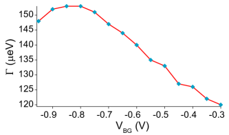
This expression applies in the limit (for ), and contains a yet undetermined prefactor , which depends on the physical quantity under consideration. To obtain the value of the charging energy , we have considered the Coulomb stability diagram of JJ1, see Appendix B.1, and extrapolated the diamond edges to large bias. Because of the large linewidth of our strongly coupled nanostructure, the determination of leads to moderate error bars, and we estimate meV. Now focusing on the differential conductance from now on, a more precise definition of is set by our choice of as the half width at half maximum of the finite bias Kondo peak. In a near equilibrium situation (corresponding to very asymmetric barrier to the left and right leads) and in the regime , we find that the unknown parameter is given by from Numerical Renormalization Group (NRG) calculations bulla2008 . However, in our experiment the conductance is tuned to its maximum value (i.e. per dot), corresponding to equally balanced tunneling amplitudes from each leads (we note that values slightly above can be achieved in our double-dot device, which we attribute to small extra elastic contributions from symmetry-broken orbital states of the carbon nanotube). In that case, decoherence of the Kondo anomaly is induced by the antagonist pinning of the Kondo resonance to the split Fermi levels of each lead, reducing the half-width of the finite-bias conductance peak compared to the equilibrium situation. For the relevant regime , one can estimate fujii_2003 a reduction by 50% of the linewidth, so that we finally fix . Because there is to date no fully controlled theory of the finite bias Kondo resonance, we believe that the unprecise choice of will introduce the largest error in our determination of , and hence of the phase boundary analyzed in Sec. III.2. The final backgate dependence of the hybridization is shown in Fig. 3 for the middle-point (particle-hole symmetric) of the Coulomb diamond of JJ1. The variations of with the backgate are quite sizeable (up to 20%), according to the exponential dependence of the Kondo scale (2) and constitute a central piece of the analysis in the superconducting state, allowing to span a large part of the phase diagram of the 0- transition. We also stress that changing the local sidegates non-only allows to tune the energy levels in the dots, as is clear in Fig. 1b), but also modifies the hybridization . The complete evolution of with backgate and sidegate voltages can be tracked by the analysis of the Kondo anomalies using Eq. (2), and leads to a greater range of variations (up to 50%).
III Experimental study of the first order 0- transition
Having characterized the normal state properties of our device, we now focus on the superconducting behavior of the nano-SQUID. Fig. 2d shows typical voltage-current characteristics obtained at three arbitrary gate voltages in the superconducting state. For all setpoints that we measured, the nano-SQUID shows an abrupt transition to the finite voltage branch indicating an underdamped device, with an hysteretic voltage-current characteristics cleuziou_2006 ; jarillo-herrero_2006 . The current at which this sharp jump occurs defines the switching current , which can be precisely determined via a digital filter liu_1995 calculating the maximum variance of the measured dc voltage, see Appendix C. Switching currents of approximately pA up to a few nA can thus be detected in a fully automated fashion.
III.1 Comparison between valence induced and Kondo induced transition
Here we focus on a comparison of the 0- transition behavior in two different correlation regimes, achieved in two distinct regions of the sidegate checkerboard diagram. Fig. 4a and Fig. 4d show both operating regions: a) corresponds to the situation already studied in the normal state, where fully developed Kondo correlations take place for the odd region of JJ1, while d) reveals an odd charge state of JJ1 where Kondo correlations do not arise (Kondo temperature smaller than the base temperature of the cryostat).
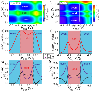
These distinct physical regime are similarly witnessed on panels b) and e), which show the normal state conductance trace along the white line in the conductance maps. In c), Coulomb blockade is fully overcome by the Kondo effect in the odd region of JJ1, while in e) Coulomb blockade is robust throughout the entire gate range. The most interesting comparison between the two regimes occurs in the superconducting state, see panels c) and f). In panel c), a supercurrent reversal (indicated by the crossing of the two curves associated to two different magnetic flux, see Eq. 1), occurs within the odd charge state of JJ1, showing that the Kondo effect plays a crucial role in triggering the transition. In contrast, panel f) shows that the supercurrent changes sign concomitantly with the increase of valence of the dot, in agreement with expectations in the strong Coulomb blockade regime glazman_1989 .
III.2 Tuning the 0- transition with controlled changes in the Kondo temperature
As shown in Sec. II.3, it is possible to tune the hybridization with the gates, which we exploit to characterize more globally the 0- transition phase boundary. Indeed, we saw previously that Kondo correlations in JJ1 are strengthened when goes from V to V in the operating region of Fig. 2a. In order to explore precisely the influence of Kondo correlations on the 0- transition, Fig. 5 presents six different plots of versus (along the white line on Fig. 2a) at different backgate voltages and magnetic fields.
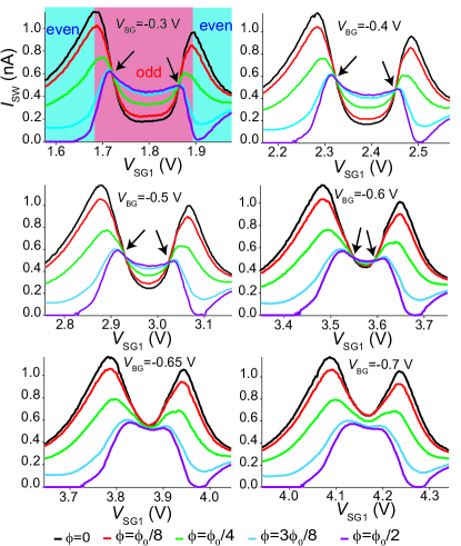
The traces exhibit two high switching current peaks corresponding to the Coulomb degeneracy points on the sides of the Kondo ridge in an odd valley of QD1. Recording such traces at different magnetic fields provides access to the flux modulation of the switching current in the nano-SQUID. Increasing the magnetic flux from 0 to leads to a steady decrease of outside the odd occupancy region of JJ1, which corresponds to a standard 0-type behavior cleuziou_2006 ; dam_2006 in the Coulomb blockaded even valleys of QD1, see Eq. 1. The flux dependence of the switching current within the odd-charge Kondo domain turns out to be more interesting, as we will analyze now. Clearly, the magnetic field behavior of is reversed deep inside the odd occupancy region of QD1, as the switching current is greater for than for , indicating a -type Josephson behavior. One can therefore identify precisely from the crossing of the switching current traces at which sidegate voltage (related to the dot energy) the behavior changes from 0 to type. This allows to define a - phase boundary for a given backgate voltage. Now, by similarly examining the characteristics at different backgate voltages (allowing to tune the linewidth ), we note that decreasing the backgate voltage (i.e. enhancing ) reduces the range for behavior, until the phase completely collapses below the critical V and a -junction is maintained all along the Kondo ridge. This physical behavior can be expected from the stronger Kondo screening at larger that tends to favor the -state. From these measurements, we can unambiguously assign a or behavior to the JJ1, as a function of both the level position and the width of QD1, as determined previously from the analysis of the normal state transport data. For all recorded transitions (corresponding to the black arrows in Fig. 5), we have extracted the corresponding microscopic parameters and , and plotted them on an experimental phase diagram shown in Fig. 6a.
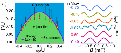
As a quantitative test of our analysis, we have displayed on Fig. 6a the theoretical phase diagram obtained from a self-consistent description of Andreev bound states meng_2009 for which corresponds to the experimentally measured meV and eV. Error bars are taking into account the uncertainty in the determination of from the finite bias Kondo resonances, see Sec. II.3. The bell-shape of the phase boundary together with the nearly quantitative comparison to theory gives strength to the interpretation of the - transition as a first order phase transition associated to the crossing of the Andreev bound states at the Fermi level clerk2000 ; bauer_2007 . A key point here is that Kondo screening is decisive to allow the existence of the 0-phase in the center of the odd charge Coulomb diamond in our experimental conditions (), see Fig. 7 in Appendix A. While the 0- transition is always related to a simple Andreev level crossing, this analysis of our data clearly demonstrates that it is the competition between the normal state Kondo temperature and the superconducting gap which determines the precise location of the 0- phase boundary bauer_2007 ; meng_2009 .
From theoretical expectations rozhkov1999 ; karrasch_2008 , a second possible smoking gun for the first order 0- phase transition lies in the anharmonic behavior (in phase) of the Josephson junction in close vicinity to the - phase boundary. This prediction motivates us to consider the field modulation of the switching current with fine changes of the backgate voltage. This is plotted on Fig. 6b, where the quantum dot level was taken in the center of the odd Kondo valley (particle-hole symmetric point , corresponding to the red star in Fig. 2a and to the fine mesh of dots in Fig. 6a). For V modulations show that JJ1 is a -junction because of the shift from those of a normal SQUID. On the contrary for V, modulations turn back to the standard behavior, indicating that JJ1 is a 0-junction. However, for the nano-SQUID switching current modulations show strong anharmonicities. For this range of backgate voltage, the critical current of JJ1 is very small, leading to a strongly asymmetric SQUID, thus JJ2 always switches at the same phase difference, implying that reflects directly the current-phase relation of JJ1 rocca_2007 . The observed non-harmonic signal could be interpreted as a further indication for the bistable behavior of the junction associated with the first order - transition rozhkov1999 ; yoshioka_2000 ; clerk2000 ; choi_2004 ; karrasch_2008 .
IV Conclusion
In conclusion, we have realized a nano-SQUID based on a superconducting carbon nanotube quantum dots that is fully tunable thanks a set of electrostatic gates, allowing a precise control of the microscopic parameters of the device. This allowed us to determine an experimental phase diagram for the - transition in the Kondo regime, which turned in good agreement with theoretical calculations based on the competition between the Kondo temperature and the superconducting gap. The observation of anharmonic behavior in the supercurrent-phase relation near the phase boundary is consistent with the first order nature of the - transition associated to the crossing of Andreev levels. Fascinating prospects offered by the present work are the control and monitoring of the - transition from supercurrent measurements, as performed here, with simultaneous local spectroscopy of the Andreev spectrum on the quantum dots in the spirit of the recent measurements of Pillet et al. pillet_2010 . Such future developments of our experiment, which seems achievable by probing the nano-SQUID with a scanning tunneling microscope, would bring strongly correlated superconducting nanostructures to a new level of control and understanding.
Acknowledgements.
We thank T. Crozes, E. Eyraud, D. Lepoittevin, C. Hoarau, and R. Haettel for their technical work, C. Thirion and R. Piquerel for their contributions in programming, and V. Bouchiat, H. Bouchiat, C. Balseiro, J.-P. Cleuziou, L. Bogani, S. Datta, D. Feinberg and T. Novotný for useful discussions. The samples were fabricated in the NANOFAB facility of the Néel Institute. This work is partially financed by ANR-PNANO projects MolNanoSpin No. ANR-08-NANO-002, ERC Advanced Grant MolNanoSpin No. 226558, and STEP MolSpinQIP.References
- (1) S. De Franceschi, L. Kouwenhoven, C. Schönenberger, and W. Wernsdorfer, Hybrid superconductor -quantum dot devices, Nature Nanotech. 5, 703 (2010).
- (2) P. Jarillo-Herrero, J. A Van Dam, and L. P Kouwenhoven, Quantum supercurrent transistors in carbon nanotubes, Nature 439, 953 956 (2006).
- (3) J. A. Van Dam, Y. V Nazarov, E. P.A.M Bakkers, S. De Franceschi, and L. P Kouwenhoven, Supercurrent reversal in quantum dots, Nature 442, 667 (2006).
- (4) J.-P. Cleuziou, W. Wernsdorfer, V. Bouchiat, T. Ondarçuhu, and M. Monthioux, Carbon nanotube superconducting quantum interference device, Nature Nanotech. 1, 53 (2006).
- (5) C. B. Winkelmann, N. Roch, W. Wernsdorfer, V. Bouchiat, and F. Balestro, Superconductivity in a single C60 transistor, Nature Physics 5, 876 (2009).
- (6) L. Hofstetter, S. Csonka,J. Nygård, and C. Schönenberger, Cooper pair splitter realized in a two-quantum-dot Y-junction Nature 461, 960 (2009).
- (7) L. G. Herrmann, F. Portier, P. Roche, A. Levy Yeyati, T. Kontos, and C. Strunk Carbon nanotubes as cooper-pair beam splitters Phys. Rev. Lett. 104, 026801 (2010).
- (8) H. Ingerslev Jorgensen, T. Novotny, K. Grove-Rasmussen, K. Flensberg, and P. E Lindelof, Critical current 0-pi transition in designed josephson quantum dot junctions, Nano Letters 7, 2441 (2007).
- (9) A. Y. Kasumov, R. Deblock, M. Kociak, B. Reulet, H. Bouchiat, I. I. Khodos, Yu. B. Gorbatov, V. T. Volkov, C. Journet, and M. Burghard, Supercurrents Through Single-Walled Carbon Nanotubes, Science 284, 1508-1511 (1999).
- (10) M. R. Buitelaar, T. Nussbaumer, and C. Schonenberger, Quantum dot in the Kondo regime coupled to superconductors, Phys. Rev. Lett. 89, 256801 (2002).
- (11) J.-P. Cleuziou, W. Wernsdorfer, V. Bouchiat, T. Ondarçuhu, and M. Monthioux, Tuning the Kondo effect with back and side gates - Application to carbon nanotube superconducting quantum interference devices and pi-junctions, Preprint arXiv:0610622 (2006).
- (12) J.-P. Cleuziou, W. Wernsdorfer, S. Andergassen, S. Florens,V. Bouchiat, T. Ondarçuhu, and M. Monthioux, Gate-Tuned High Frequency Response of Carbon Nanotube Josephson Junctions, Phys. Rev. Lett. 99, 117001 (2007).
- (13) E. Pallecchi, M. Gaass, D. A. Ryndyk, and Ch. Strunk, Carbon nanotube Josephson junctions with Nb contacts, Appl. Phys. Lett. 93, 072501 (2008).
- (14) K. Grove-Rasmussen, H. I. Jørgensen, B. M. Andersen, J. Paaske, T. S. Jespersen, J. Nyg rd, K. Flensberg, and P. E. Lindelof, Superconductivity-enhanced bias spectroscopy in carbon nanotube quantum dots, Phys. Rev. B 79, (2009).
- (15) A. Eichler, R. Deblock, M. Weiss, C. Karrasch, V. Meden, C. Schonenberger, and H. Bouchiat, Tuning the Josephson current in carbon nanotubes with the Kondo effect, Phys. Rev. B 79, (2009).
- (16) Y. Kanai, R. S. Deacon, A. Oiwa, K. Yoshida, K. Shibata, K. Hirakawa, and S. Tarucha, Electrical control of Kondo effect and superconducting transport in a side-gated InAs quantum dot Josephson junction, Phys. Rev. B 82, 54512 (2010).
- (17) C. W. J. Beenakker, and H. van Houten, Single-Electron Tunneling and Mesoscopic Devices (Springer, Berlin, 1992).
- (18) A. V. Rozhkov and D. P Arovas, Josephson coupling through a magnetic impurity, Phys. Rev. Lett. 82, 2788 (1999).
- (19) A. A. Clerk, and V. Ambegaokar, Loss of -junction behavior in an interacting impurity Josephson junction, Phys. Rev. B 61, 9109 (2000).
- (20) T. Yoshioka, and Y. Ohashi, Numerical renormalization group studies on single impurity Anderson model in superconductivity: a unified treatment of magnetic, nonmagnetic impurities, and resonance scattering, J. Phys. Soc. Japan 69, 1812 (2000).
- (21) E. Vecino, A. Martin-Rodero, and A. Levy Yeyati, Josephson current through a correlated quantum level: Andreev states and junction behavior Phys. Rev. B 68, 035105 (2003).
- (22) F. Siano, and R. Egger, Josephson current through a nanoscale magnetic quantum dot, Phys. Rev. Lett. 93, 047002 (2004).
- (23) M. S. Choi, M. Lee, K. Kang, and W. Belzig, Kondo effect and Josephson current through a quantum dot between two superconductors, Phys. Rev. B 70, 020502 (2004).
- (24) G. Sellier, T. Kopp, J. Kroha, and Y. S. Barash, -Junction behavior and Andreev bound states in Kondo quantum dots with superconducting leads, Phys. Rev. B 72, 174502 (2005).
- (25) Tomas Novotny, Alessandra Rossini, and Karsten Flensberg, Josephson current through a molecular transistor in a dissipative environment, Phys. Rev. B 72, 224502 (2005).
- (26) J. Bauer, A. Oguri, and A. C. Hewson, Spectral properties of locally correlated electrons in a Bardeen-Cooper-Schrieffer superconductor, J. Phys.: Condens. Matter 19, 486211 (2007).
- (27) C. Karrasch, A. Oguri, and V. Meden, Josephson current through a single Anderson impurity coupled to BCS leads, Phys. Rev. B 77, 024517 (2008).
- (28) T. Meng, S. Florens, and P. Simon, Self-consistent description of Andreev bound states in Josephson quantum dot devices, Phys. Rev. B 79, 224521 (2009).
- (29) L. I. Glazman, and K. A. Matveev, Resonant Josephson current through Kondo impurities in a tunnel barrier, JETP Lett. 49, 659 (1989).
- (30) L. Kouwenhoven, and L. Glazman, Revival of the Kondo effect, Phys. World 14, 33 (2001).
- (31) Liu, W. Y., Magnin, I. E. & Gimenez, G. A New Operator for the Detection of Transitions in Noisy Signals, Traitement du Signal 12, 225 (1995).
- (32) H. Grabert, and M. H. Devoret, Single Charge Tunneling, Plenum press, New York, 1992.
- (33) F. D. M. Haldane, Scaling Theory of the Asymmetric Anderson Model, Phys. Rev. Lett. 40, 416 (1978).
- (34) R. Bulla, T. A. C. Costi, and T. Pruschke, Numerical renormalization group method for quantum impurity systems, Rev. Mod. Phys. 80, 395 (2008).
- (35) T. Fujii, and K. Ueda, Perturbative approach to the nonequilibrium Kondo effect in a quantum dot, Phys. Rev. B 68, 1 (2003).
- (36) D. Goldhaber-Gordon, J. G res, M. Kastner, Hadas Shtrikman, D. Mahalu, and U. Meirav, From the Kondo Regime to the Mixed-Valence Regime in a Single-Electron Transistor, Phys. Rev. Lett. 81, 5225 (1998).
- (37) M. Della Rocca, M. Chauvin, B. Huard, H. Pothier, D. Esteve, and C. Urbina, Measurement of the Current-Phase Relation of Superconducting Atomic Contacts, Phys. Rev. Lett. 99, 127005 (2007).
- (38) J.-D. Pillet, C. H. L. Quay, P. Morfin, C. Bena, A. Levy Yeyati, and P. Joyez, Andreev bound states in supercurrent-carrying carbon nanotubes revealed, Nature Physics 6, 965 (2010).
Appendix A Theoretical analysis of the phase diagram
A.1 Model for a superconducting quantum dot
The standard Hamiltonian to describe a single superconducting quantum dot is given by the superconducting Anderson model
| (3) |
where
In the above equations, is the annihilation operator of an electron with spin on the dot, that of an electron with spin and wave vector in the lead , and . The leads are described by standard s-wave BCS Hamiltonians with superconducting gaps . The phase difference of the latter is noted . Furthermore, the leads are assumed to have flat and symmetric conduction bands, i.e. the kinetic energy measured from the Fermi level ranges in and the density of states is . We assume -independent and symmetric tunneling amplitudes between the dot and both superconducting leads. The dot is described by a single energy level submitted to the Coulomb interaction (in our convention vanishes at the center of the Coulomb diamond).
A.2 Renormalized Andreev Bound states and phase diagram of the - transition
In the superconducting state, the four atomic states of the quantum dot evolve onto renormalized Andreev bound states (ABS) that possibly live within the gap. A quantitative description of this process was proposed in Ref. meng_2009, , starting with bare values of the ABS splitting in the limit of infinite gap:
| (4) | |||||
| (5) |
with
| (6) |
In this simplified (and unrealistic) limit, the / transition corresponds to the crossing of the and states, which occurs for , leading to a dome-like shape in the (,) plane. However, the phase boundary quantitatively depends on the precise value of the superconducting gap , which must be more realistically included in the calculation. This is done by calculating the corrections at order to the ABS positions meng_2009 , followed by a self-consistency loop that takes into account the leading logarithmic singularities:
| (7) | |||||
and
| (8) | |||||
with , and have been defined in Eqs. (4)-(5). The numerical resolution of the self-consistent equation (7) provides an accurate determination of the phase boundary under the condition , that we successfully compared to the experimental data. Note that we corrected here a misprint in Ref. meng_2009, , namely a factor 2 in front of the second term within the integral in (7)-(8).
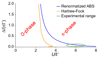
In order to stress the key role of the Kondo effect for the 0- transition in our experimental conditions, we compare the phase diagram at particle-hole symmetry () obtained from the renormalized-ABS theory meng_2009 and from static Hartree-Fock mean-field theory rozhkov1999 , see Fig. 7. Because the renormalized-ABS approach includes the Kondo scale (at one-loop order), it allows the extension of the 0- boundary for arbitrary large values of . In contrast, the static mean-field approach is unable to restore a -state for Coulomb interaction such that , and fails to reproduce our experimental observation of a supercurrent reversal in the regime . This comparison shows that the phase boundary in our experiment is indeed associated to a competition between the normal state Kondo temperature and the superconducting gap, in agreement with theoretical expectations bauer_2007 ; meng_2009 .
Appendix B Determination of the microscopic parameters of the nanosquid
B.1 Charging energy
Because the charging energy in a carbon nanotube quantum dot results from the confinement between fixed contacts, one does not expect large variations of for small detuning of the backgate. In order to determine the experimental phase diagram for the transition, an estimate of is required. This is obtained by considering the Coulomb stability diagram of JJ1 for two different values of the backgate, see Fig. 8, and extrapolating the diamond edges to large bias.

Because of the large linewidth of our strongly coupled nanostructure, the determination of also contains sizeable error bars, which we estimate as meV.
B.2 Proximity gap
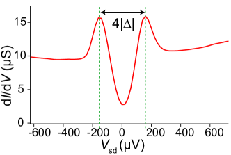
Current-bias measurements were performed in order to directly access both the superconducting switching current and the differential conductance of the nano-SQUID at mK. In the presence of superconductivity, the two cotunneling peaks associated with quasiparticle current in the differential conductance buitelaar_2002 appear at V, where 2 is the superconducting gap provided by the proximity effect on the nanotube, see Fig. 9. This allows to extract the superconducting gap in our device, eV, which is reduced from the bulk value of eV for aluminum, due to the thin palladium contact layer between the carbon nanotube and the aluminum electrodes.
Appendix C Switching current detection
In order to have an accurate method to extract the switching current from voltage/current characteristics, even for small transition voltage jumps to the dissipative state, we have implemented a digital filter based on the work of Liu et al. liu_1995 . The main purpose of this filter is the detection of transitions from noisy signal, which we apply to the superconducting/ normal transition. The operation consists in estimating the variance of the first order moment of the signal in a sliding window. A schematic view of the filter is presented in Fig. 10a. The first order moment is estimated to begin with via a classic averaging filter in a sliding window characterized by the impulse response with the normalised rectangular function and the filter length. Finally the estimated variance is obtained by - with another averaging filter of length . For the switching current detection with a sample rate of one thousand, we have taken . Such filter provides a sharp signal from the steplike features of our voltage/current characteristics as presented n Fig. 10b.
