High-Q optomechanical GaAs nanomembranes
Abstract
We present a simple fabrication method for the realization of suspended GaAs nanomembranes for cavity quantum optomechanics experiments. GaAs nanomembranes with an area of by and a thickness of are obtained by using a two-step selective wet-etching technique. The frequency noise spectrum reveals several mechanical modes in the kilohertz regime with mechanical -factors up to at room temperature. The measured mechanical mode profiles agree well with a taut rectangular drumhead model. Our results show that GaAs nanomembranes provide a promising path towards quantum optical control of massive nanomechanical systems.
pacs:
42.50.Ct,68.60.Bs,78.66.FdQuantum optomechanics has become an emerging field with the goal of engineering and detecting quantum states of massive mechanical systems such as the quantum ground stateTeufel2011 ; Wilson-Rae2007 ; Marquardt2007 or entangled quantum statesVitali2007 ; Hammerer2009 . In this rapidly expanding field, various materials and geometries are being pursued, in order to control the coupling between phonons and photonsKippenberg2008 ; Marquardt2009 ; Favero2009 .
Incorporating direct band gap semiconductor materials in optomechanics exhibits new prospects due to a number of advantageous properties. In particular, GaAs enables the integration of optoelectronic functionality with nanomechanical elementsUkita1993 . The noncentrosymmetric nature of the zinc-blende crystal structure of GaAs results in an appreciable piezoelectric coefficient, enabling efficient actuation or transductionMasmanidis2007 . Furthermore, there is a proposal of cooling the lattice temperature of semiconductors down to 10 K, referred to as optical refrigeration, although experimental demonstrations have not yet been realizedSheik-Hahae2007 . Quantum dots embedded in GaAs also enable strong coupling between a photon and a confined exciton.Yoshie2004 . Much effort has been invested in fabricating GaAs-based micro-resonatorsCole2008 ; Cole2010a and improving their mechanical properties by strain engineering Yamaguchi2008 . Coupling the intrinsic physical properties of direct band gap semiconductors to mechanical modes would enable a multitude of effects within cavity quantum optomechanics engineeringMidolo2011 . Very recent results on both GaAs disk resonators and InP photonic crystal cavities show the feasibility of realizing optomechanical systems in direct band gap semiconductorsDing2010 ; Gavartin2011 but it is widely observed that GaAs microresonators suffer from low -factors, which limit the optomechanical cooling performance. Here, we present a simple fabrication method for GaAs nanomembranes and demostrate that they exhibit high mechanical -factors.

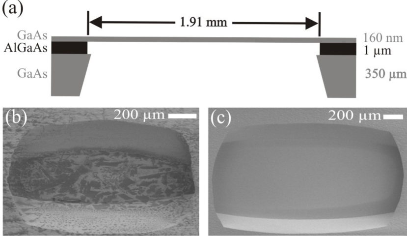
The GaAs membrane is fabricated from a GaAs/AlGaAs heterostructure wafer comprised of a (100)-oriented GaAs substrate (thickness: ), etch stop layer (thickness: ), and a GaAs capping layer (thickness: ), which is shown in Fig. 1(a). The first step is to remove the substrate with selective citric acid wet-etching by using AlGaAs as an etch stop layerkim1998 . Then a hydrofluoric acid (HF) selective wet-etching follows in order to remove the AlGaAs sacrificial layerYablonovitch1989 . The nanomembranes made by our method are optically accessible from both sides, which enables implementing cavity optomechanical cooling schemes.
The detailed fabrication process is as follows: photoresist with a thickness of is coated on both sides of the wafer and the patterns of the holes with different diameters ranging from to are defined by photolithography. After 30 minutes hard baking at a temperature of C on a hotplate, the wafer is immersed into citric acid/ solution (4 Citric acid (50% by wt.)/1 (30%))kim1998 with magnetic stirring for 20 hours to etch through the GaAs substrate. Thanks to the excellent etch rate selectivity for GaAs versus AlGaAs in the citric acid/ solution, the GaAs layer is intact due to the protection of the AlGaAs layer and the photoresist during the citric acid wet-etching. Once the substrate is etched away, another selective wet-etching follows to remove the AlGaAs sacrificial layer and finally a GaAs nanomembrane is formed after removing the photoresist.

We have observed that often a thin layer of photoresist and submicron-sized particles are left after the completion of photoresist removal, which is shown by the scanning electron micrograph (SEM) in Fig. 1(b). These residues can be significant sources of light scattering and deteriorations of mechanical -factors. The remnant resist can only be removed by oxygen plasma while the submicron-sized particles speculated to be hydroxide of aluminiumKhankhoje2010a can be removed in potassium hydroxide (KOH) solutions. Fig. 1(c). shows SEM of a nanomembrane after the oxygen plasma and KOH cleaning processes. We found that the shapes of the fabricated nanomembranes deviated significantly from the circular photolithography masks. This comes from the different etch rates for different crystallographic planes of GaAs in citric acid. A close inspection of the membranes reveals that they are not completely flat, but rather they are bowing with an amplitude at the center of the membranes on the order of a few microns. The size of the largest nanomembrane made by our method is roughly by .
| Mode | Frequency (kHz) | -factor () | () |
|---|---|---|---|
| (2,1) | 23.4 | 0.50 | 0.12 |
| (3,2) | 45.5 | 0.56 | 0.25 |
| (4,1) | 47.5 | 0.53 | 0.25 |
| (4,3) | 59.5 | 2.3 | 1.4 |
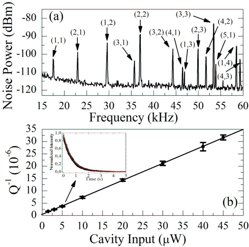
We have characterized the mechanical properties of the nanomembranes via frequency noise spectrum by using cavity transmission measurements. A dielectric concave mirror and a 160-nm-thick GaAs membrane form a cavity with the measured finesse of about 10. By feeding the spectrum analyzer with the RF signal from the photodiode, we have observed 14 resonance frequencies ranging from 17.5 kHz (the (1,1)-mode) to 59.5 kHz ((4,3)-mode), see Fig. 2(a). The -factor is defined as = where is the resonance frequency and is the mechanical damping rate. is measured through a ringdown measurement in which the ringdown of the mechanical modes is observed by inducing the oscillations with an intensity-modulated cavity field. A typical ringdown measurement for the (4,3)-mode is shown in the inset of Fig. 2(b). Due to the optomechanical effectKippenberg2008 ; Marquardt2009 ; Favero2009 in the ringdown measurements where the -factors and resonance frequencies vary with input powers, the intrinsic mechanical -factor of the (4,3)-mode is extracted from the power-dependent ringdown measurement in Fig. 2(b). By extrapolating the -factor data to zero cavity input power, a -factor of is found at 59.5 kHz. Since the damping rate of a mechanical mode (i.e., inverse of Q) generally scales linearly with , is an important parameter for the mechanical characterizations. Table 1 lists the resonance frequencies, the corresponding -factors and the product of and for the modes we have carefully characterized. The highest value in our case is , which is comparable to the state of art for GaAs resonators at cryogenic temperatures, cf. Ref. Yamaguchi2008, . We stress that much higher -factors for our GaAs nanomembranes are expected at cryogenic temperatures.

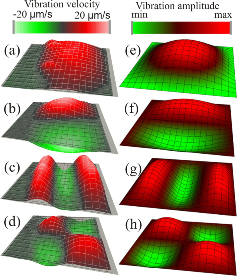
The vibration amplitudes, which are proportional to the vibration speeds for a given resonance frequency, are mapped by a laser-Doppler vibrometer [MSA-500 Micro System Analyzer (Polytec Ltd)] with a white light interferometry method. Due to space limitations in the experimental method, these measurements were performed on a smaller sample (roughly by ) than the one presented in Fig. 1(c). The vibration profiles of the (1,1), (1,2), (3,1), and (2,2)-modes are shown on the left-hand side of Fig. 3 while the corresponding numerical simulations are on the right-hand side. The simulated vibration modes are based on a taut rectangular drumhead model. We find a good agreement between measured mechanical mode profiles and simulations. This model is also used to estimate the fundamental resonance frequency. The internal stress of the AlxGa1-xAs/GaAs interface due to the lattice mismatch during growth can be approximated asHjort1994157 and in our case = 0.85. Thus a tensile stress of 110 MPa is predicted. By including this stress, we get a fundamental resonance frequency (the (1,1)-mode) of 63 kHz which is higher than the measured resonance frequency. More investigations are needed to obtain a better understanding of the relation between the stress and high -factors in this system.
In conclusion, we have realized high- GaAs nanomembranes with unprecedented sizes for cavity quantum optomechanics experiments. The resonance frequencies and mode profiles are both theoretically and experimentally investigated. Experimental data show good agreement with a simplified model based on a taut rectangular drumhead. The ringdown measurements reveal that the highest -factors of the mechanical modes can be up to at room temperature, which underlines the potential of these nanomembranes for cavity cooling experiments. We will report on such studies in a future publication. Further steps can be envisioned by incorporating semiconductor quantum dots in nanomembranes to cool the nanomechanical modes to its ground stateWilson-Rae2004 and patterning the nanomembranes for controlling of the coupling between phonons and photonsAlegre2010 .
We gratefully acknowledge S. Schmid and A. Boisen for the assistance of vibration profile measurements and financial support from the Villum Kann Rasmussen Foundation, The Danish Council for Independent Research (Natural Sciences and Technology and Production Sciences), the European Research Council (ERC consolidator grant), and the European project Q-ESSENCE.
References
- (1) J. D. Teufel, T. Donner, D. Li, J. W. Harlow, M. S. Allman, K. Cicak, A. J. Sirois, J. D. Whittaker, K. W. Lehnert, and R. W. Simmonds. Nature 475, 359 (2011).
- (2) I. Wilson-Rae, N. Nooshi, W. Zwerger, and T. J. Kippenberg. Phys. Rev. Lett. 99, 093901 (2007).
- (3) F. Marquardt, J. P. Chen, A. A. Clerk, and S. M. Girvin. Phys. Rev. Lett. 99, 093902 (2007).
- (4) D. Vitali, S. Gigan, A. Ferreira, H. R. Böhm, P. Tombesi, A. Guerreiro, V. Vedral, A. Zeilinger, and M. Aspelmeyer. Phys. Rev. Lett. 98, 030405 (2007).
- (5) K. Hammerer, M. Aspelmeyer, E. S. Polzik, and P. Zoller. Phys. Rev. Lett. 102, 020501 (2009).
- (6) T. J. Kippenberg and K. J. Vahala 321, 1172 (2008).
- (7) F. Marquardt and S. Girvin. Physics 2 (2009).
- (8) I. Favero and K. Karrai. Nature Photonics 3, 201 (2009).
- (9) H. Ukita, Y. Uenishi, and H. Tanaka. Science 260, 786 (1993).
- (10) S. C. Masmanidis, R. B. Karabalin, I. De Vlaminck, G. Borghs, M. R. Freeman, and M. L. Roukes. Science 317, 780 (2007).
- (11) M. Sheik-Bahae and R. I. Epstein. Nature Photon. 1, 693 (2007).
- (12) T. Yoshie, A. Scherer, J. Hendrickson, G. Khitrova, H. M. Gibbs, G. Rupper, C. Ell, O. B. Shchekin, and D. G. Deppe. Nature 432, 200 (2004).
- (13) G. D. Cole, S. Gröblacher, K. Gugler, S. Gigan, and M. Aspelmeyer. Appl. Phys. Lett. 92, 261108 (2008).
- (14) G. D. Cole, Y. Bai, M. Aspelmeyer, and E. A. Fitzgerald. Appl. Phys. Lett. 96, 261102 (2010).
- (15) H. Yamaguchi, K. Kato, Y. Nakai, K. Onomitsu, S. Warisawa, and S. Ishihara. Appl. Phys. Lett. 92, 251913 (2008).
- (16) L. Midolo, P. J. van Veldhoven, M. A. Dündar, R. Nötzel, and A. Fiore. Appl. Phys. Lett. 98, 211120 (2011).
- (17) L. Ding, C. Baker, P. Senellart, A. Lemaitre, S. Ducci, G. Leo, and I. Favero. Phys. Rev. Lett. 105, 263903 (2010).
- (18) E. Gavartin, R. Braive, I. Sagnes, O. Arcizet, A. Beveratos, T. J. Kippenberg, and I. Robert-Philip. Phys. Rev. Lett. 106, 203902 (2011).
- (19) J.-H. Kim. J. Vac . Sci. Technol. B 16, 558 (1998).
- (20) E. Yablonovitch, T. Gmitter, J. P. Harbison, and R. Bhat. Appl. Phys. Lett. 51, 2222 (1989).
- (21) U. K. Khankhoje, S.-H. Kim, B. C. Richards, J. Hendrickson, J. Sweet, J. D. Olitzky, G. Khitrova, H. M. Gibbs, and A. Scherer. Nanotechnology 21, 065202 (2010).
- (22) K. Hjort, F. Ericson, J. A. Schweitz, C. Hallin, and E. Janzn. Thin Solid Films 250, 157 (1994).
- (23) I. Wilson-Rae, P. Zoller, and A. Imamoglu. Phys. Rev. Lett. 92, 075507 (2004).
- (24) T. P. M. Alegre, A. Safavi-Naeini, M. Winger, and O. Painter. Opt. Express 19, 5658 (2011).