Relating Hysteresis and Electrochemistry in Graphene Field Effect Transistors
Abstract
Hysteresis and commonly observed p-doping of graphene based field effect transistors (FET) was already discussed in reports over last few years. However, the interpretation of experimental works differs; and the mechanism behind the appearance of the hysteresis and the role of charge transfer between graphene and its environment are not clarified yet. We analyze the relation between electrochemical and electronic properties of graphene FET in moist environment extracted from the standard back gate dependence of the graphene resistance. We argue that graphene based FET on a regular SiO2 substrate exhibits behavior that corresponds to electrochemically induced hysteresis in ambient conditions, and can be caused by charge trapping mechanism associated with sensitivity of graphene to the local pH.
pacs:
72.80.Vp, 85.30.TvI Introduction
Graphene, as a single atom thick layer of carbon atoms, has already showed potential for application in electronics and biosensingRatinac et al. (2010). However graphene as a truly 2D system is ultrasensitive Schedin et al. (2007) to the underlying substrate and surface chemistry, which alters the charge transport properties of pristine graphene. One of the main issues in graphene devices is a hysteretic behavior of its resistance observed in ambient conditions, when a gate voltage is swept back and forth. The presence of hysteresis and commonly observed p-doping of graphene based field effect transistors (FET) was already discussed in recent reportsLafkioti et al. (2010); Wang et al. (2010); Sabri et al. (2009); Levesque et al. (2011). The interpretation of experimental works differs; and the mechanism behind the appearance of hysteresis and the role of charge transfer between graphene and its environment are not clarified yet.
In an ideal case of grounded graphene its charge neutrality point (CNP) is located at zero back gate voltage. However, in ambient conditions most of the graphene based FETs show initial p-doping (CNP is positioned at positive Vg) and hysteresis. We point out that these two effects can be related but do not necessarily have the same nature. The doping of graphene can be caused either by the adsorbates on top or underneath the graphene surfaceSchedin et al. (2007); Lafkioti et al. (2010); Wang et al. (2010) or by the electrochemical processes involving grapheneSabri et al. (2009); Levesque et al. (2011); Sidorov et al. (2011). Depending on the nature of the dopant or the electrochemical environment, the initial doping can be either p or n, which introduces a shift of the graphene CNP to positive or negative gate voltages respectively. One should keep in mind that even in the absence of a net doping the dynamic response of the graphene resistance, namely hysteresis, can be different.
There are two types of directions defined for hysteresis; positive and negative Wang et al. (2010). The positive direction of hysteresis corresponds to the CNP shifting towards negative voltages while the gate voltage is swept further into the negative regime. In case of negative hysteresis the shift of the resistance with respect to the gate voltage is in the opposite direction: the CNP shifts toward more positive values while sweeping the gate into the negative regime. Wang et al.Wang et al. (2010) proposed that negative and positive hysteresis directions can be attributed to two competing mechanisms: capacitive coupling and charge trapping from/to graphene, respectively.
Capacitive coupling enhances the local electrical field near graphene, inducing more charge carriers and causing a negative direction of hysteresis. An example of a mechanism for capacitive coupling is a dipole layer placed in between graphene and the back gate. In moist air and without additional treatment of the silicon oxide substrate (a common insulator for a GFET) this dipole layer exists as adsorbed water molecules at room temperature Moser et al. (2008); Lafkioti et al. (2010) or ordered ice at low temperatureWang et al. (2010); Wehling, Lichtenstein, and Katsnelson (2008). The capacitive coupling mechanism is also dominant in electrolyte-gating devices, via ions in the electrical double layer Wang et al. (2010). The positive direction of hysteresis is caused by a charge trapping mechanism. Accumulated charge in trap centers will start screening the electric field of the back gate. One of the examples of trap centers are surface states in between SiO2 and graphene Wang et al. (2010); Romero et al. (2008); Liao et al. (2010); Shin, Seo, and Cho (2011). In case of graphene based FET traps in bulk SiO2 or SiO2/Si interface were excluded in a recent report by Lee et al.Lee et al. (2011), who measured time scales which were too fast for these types of trapped centers.
A separate charge transfer mechanism which was observed for the hydrogenated surface of diamond Chakrapani et al. (2007), carbon nanotubes Aguirre et al. (2009) and graphene based FETs Sabri et al. (2009); Levesque et al. (2011); Sidorov et al. (2011), is the dissociation of adsorbed water and oxygen on the carbon surface. Since water in equilibrium with air is slightly acidic (pH=6), the electrochemical potential of the carbon surface is higher than that of the solution, resulting in electron transfer from graphene. Therefore, a graphene FET possesses a net p-doping in moist air. The electron transfer is mediated by oxygen solvated in water and can occur in opposite direction with increasing pH. This redox can therefore influence the dynamic response of graphene devices under an applied back gate and cause a positive hysteresis.
A recent report by Fu et al.Fu et al. opened the discussion whether graphene pH sensitivity is caused by charge transfer directly between graphene and the solution Ang et al. (2008); Ohno et al. (2009); Heller et al. (2010) or if the sensitivity is mediated by a layer on top or next to graphene (either oxide or polymer residue). This layer can provide terminal hydroxyl groups which can be protonized or deprotonized depending on the proton concentration in the solution (pH), yielding a bound surface charge layer, which can electrostatically induce carriers in graphene. Recently it was reported that application of a gate potential can lead to a local change of pH in a thin water film next to an oxide substrate Veenhuis et al. (2009). We argue that a combination of these two effects can result in a positive hysteresis in graphene, where the residues act as mediators for charge trapping actuated by pH changes induced via gate electrical field. We emphasize that both cases, independent whether the charge trapping is direct or mediated by residues, would lead to the same direction in hysteresis and will be undistinguishable in transport experiments. Though replacement of the silicon oxide with either a hydrophobic Lafkioti et al. (2010); Shin, Seo, and Cho (2011) or an oxygen free Sabri et al. (2009) substrate did show suppression of both initial p-doping and hysteretic behavior, none of the reports link the chemical redox to the direction of hysteresis.
In this work we analyze the relation between electrochemical and electronic properties of graphene FET in moist environment. We argue that graphene based FET on a regular SiO2 substrate exhibits behavior that corresponds to electrochemically induced hysteresis in ambient conditions, caused by charge trapping mechanisms associated with the sensitivity of graphene to the local pH.
II Methods
Samples were obtained by mechanical exfoliation of graphite (Highly Ordered Pyrolytic Graphite or Kish) on an oxidized n+-doped silicon substrate (300 or 500 nm thick oxide layer), which functions as a back gate. The SiO2 wafers are commercially available from Silicon Quest International, where the oxide is prepared by dry oxidation. Single layer graphene flakes were chosen based on their optical contrast and thickness measured by atomic force microscopy. A small number of samples were inspected with Raman spectroscopy to verify the number of layers. Ti/Au (5/40 nm thick) electrodes were prepared using standard electron beam lithography and lift off techniques. For electrical measurements samples are placed in a vacuum can with base pressure of mbar, using a standard low frequency AC lock-in technique with an excitation current of 100 nA. The carrier density in graphene is varied by applying DC voltage (Vg) between the back gate electrode and the graphene flake, as depicted in Fig. 1(a). The charge carrier mobilities () ranged from 2.500 up to 5.000 cm2/Vs at a charge carrier density of .
The sensor properties of the devices were studied in the following way. First, we pumped down the sample can (95 cm3 in volume) to the base pressure. Then a valve connecting the can to a volume, containing liquid water and filled with saturated vapor (H2O or D2O at 32 mbar saturation pressure) at 25 Co, was kept open for 1 s (short exposure to the vapor). After measurement, the valve to the sample was fully opened, connecting the sample volume to the water container (flooding with water vapor). In case of ethanol vapor exposure the procedure was kept the same, but the partial pressure of ethanol in the liquid cavity was 78 mbar. The purity of heavy water and ethanol was 99.9%. A graphene based FET on a hydrophobic substrate was also prepared by exposure of SiO2 to hexamethyldisilazane (HMDS) vapor prior to graphene deposition. HMDS forms a self assembled monolayer which protects graphene from the influence of dangling bonds in silicon dioxide and prevents adsorbtion of water molecules in the vicinity of graphene.
III Results and discussion
In ambient conditions the devices appear to be p-doped, with a pronounced positive hysteresis in the dependence of resistivity versus gate voltage (not shown). To remove adsorbates from the graphene surface we perform global annealing of the device in vacuum at 130oC for 1,5 hrs. After annealing, the gate dependence does not show hysteresis and becomes symmetric around the CNP (Fig. 1(c)), which is located at a negative gate voltage (-11 V), indicating electron doping. Similar shifts towards negative gate voltages were observed by Romero et al.Romero et al. (2008) and associated with SiO2 surface states. We will call this position of the charge neutrality point the initial position (after annealing). Short exposure to water does not cause hysteresis, but reduces by 25 % compared to the initial state and can be attributed to the increase of a number of the scatter centers for charge carriersSchedin et al. (2007) (Fig. 1(d)). Since graphene is hydrophobic, we assume that during the short exposure adsorbates only occasionally agglomerate on the graphene surface in the vicinity of polymer leftovers which are unavoidably present after the lithography step (Fig. 1(a)).
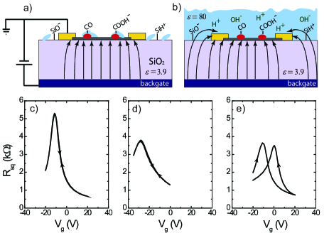
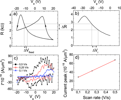
Flooding the sample chamber with H2O vapor assures full coverage of the previously annealed SiO2 and graphene surface with a thin film of water ( 3 nm thick Kim (2010)), similar to ambient conditions. After flooding we observe both electron-hole asymmetry and a highly hysteretic behavior of the graphene device, where the CNP for trace and retrace are situated at Vg of opposite signs (Fig. 1(e)). Moreover, a decrease of the scanning rate in gate voltage sweeps (V/s) leads to more pronounced hysteresis with the spacing between trace and retrace maxima increasing from 6.5 V at 1 V/s up to 23,5 V for 0,1 V/s. The cycle of annealing and water exposure was repeated a few times showing reproducible results. The positive direction of hysteresis indicates charge trapping mechanism, while electron -hole asymmetry can be explained in two ways: real asymmetry due to doping of graphene under the contactsHuard et al. (2008) or an artifact of charging and discharging graphene due to the hysteresis. Since we do not observe asymmetry in the initial curve, the latter situation will be assumed in further discussions.
Next, we present a novel analysis of hysteretic back gate voltage sweeps from the point of view of time dependent shifts in CNP. These shifts represent a change in carrier density within a certain time, equivalent to a current. We estimate this current corresponding either to the charge flow in or out of graphene, or induced charge, in the following way. Charge current is extracted by comparing the non hysteretic Dirac curve of graphene, which is shortly exposed to water vapor, to the curves after the sample is flooded, measured at different scan rates: 0,5; 0,25 and 0,1 V/s. The exact procedure is shown in Fig. 2a), b). For each scan rate the gate voltage axis was divided into fixed regions . A change in voltage induces a change in the carrier density and resistance accordingly. Due to the charge trapping mechanism induced by water, the same will require a different value of gate voltage in case of the non-hysteretic curve. The difference between and will be proportional to the amount of additionally induced or transferred charge in graphene. The charge current (A/m2) in graphene can then be calculated as:
| (1) |
where is the elementary charge, with the charge capacitance per unit area for 500 nm SiO2, and is the scan rate of the gate sweep (V/s).
The calculated charge current curves (Fig. 2(c))
resemble the electrovoltaic characteristics of graphene based
electrochemical cells with controlled pH Fu et al. . A graphene based
device on a SiO2 substrate can act as a working electrode in the
thin layer of water covering the hydrophilic oxide surface. Thus we
can consider graphene based devices as electrochemical cells.
Moreover, the height of the observed peaks scales linearly with the
scan rate of the applied gate voltage (Fig. 2(d))
which, for an electrochemical cell, suggests that these peaks
originate from a non-Faradaic or non-diffusion limited process
involving the adsorbed ions on the graphene surfaceAng et al. (2008).
We performed the same sequence of experiments with graphene devices
on HMDS primed SiO2. In contrast to graphene on hydrophilic
SiO2 we observe neither hysteresis nor any changes in the
graphene resistance under water vapor exposure.
From the fact that the initial curve (after annealing) has no hysteresis we can exclude charge trapping in the surface states of SiO2. Comparing to a local current annealing procedure Wang et al. (2010), here we globally annealed the sample which assures desorption of H2O molecules from the whole SiO2 surface and prohibits their diffusion back to the graphene surface. The hysteresis appears only when the amount of water in the system is high enough to form a continuous layer. The linear scaling of extracted height of current peaks with scan rate indicates the reversible charging of an ionic layer at the graphene surface (electrode) by an applied gate voltage. The absence of hysteresis of the graphene resistance when HMDS is used supports the idea that the trapping mechanism happens by the presence of a water layer on the SiO2 surface. The dielectric constant of water is much higher than . Therefore the electrical field lines in the device deviate from plane capacitor and can be present in the water layer (Fig. 1(b)). The strong electrical field across the water layer can either cause dissociation of water molecules Teoh et al. (2011) or proton release/uptake by terminal OH- groups at the oxide surface, as previously describedFu et al. ; Veenhuis et al. (2009). Both these mechanisms lead to a local pH change in the graphene vicinity. Depending on the pH, the dangling bonds of the oxide or polymer remains on graphene will change their charge state, inducing an opposite charge in grapheneFu et al. ; Teoh et al. (2011). At the present state we can not pinpoint the exact identity of the ionic species causing the change of environment around the graphene. A possible electrochemical reaction on the unprotected Au electrodes is not relevant as this was ruled out by Wang at alWang et al. (2010). where both samples with protected and unprotected gold contacts showed the same type of hysteresis.
Since the dipole nature of water molecules is often discussed in relation to the hysteresis observed in graphene devices Wang et al. (2010); Lafkioti et al. (2010); Wehling, Lichtenstein, and Katsnelson (2008), we decided to study the response of graphene resistance to ethanol vapors. A pure neutral ethanol solution has at least 100 times less concentration of H+ and OH- ions than pure waterHansen (2007). However the dipole moment of an ethanol molecule is comparable to that of water Hansen (2007), which makes it possible to separate the electrochemical from electrostatic influences on the charge carrier density in graphene. In Fig. 3(a,b) the changes in graphene resistivity under ethanol vapor exposure are presented. Except for the reduction of charge carrier mobility by 25 % (comparable to water exposure) neither considerable hysteresis nor doping were observed.
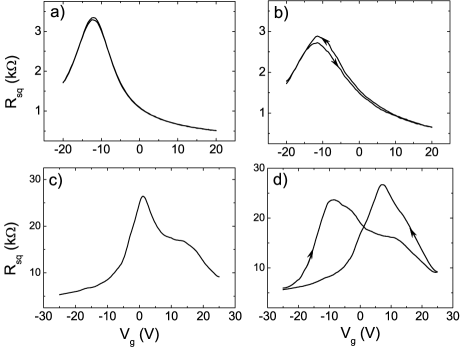
We also performed similar experiments using D2O vapor with another set of samples. Chemically, D2O molecules behave similar to H2O. However, D+ ions are two times heavier than H+, whereas the relative increase in mass of OD- ions compared to OH- is negligible. If the electrochemical process on graphene surface is proton diffusion limited, one expects to observe a different behavior of the hysteresis at various scan rates. Experimentally we do not observe any significant difference in graphene’s response between H2O and D2O. Heavy water exposure causes doping and direction of the hysteresis comparable to normal water values (Fig. 3(c,d)).
Our experiment with ethanol vapor supports the idea that the polarity of molecules adsorbed in the graphene vicinity does not influence the dynamic response of graphene resistance to a gate voltage. We suggest that the main reason of the observed hysteresis in ambient conditions is the electrochemical activity of water molecules in the graphene environment.
IV Conclusions
In conclusion, we have shown that the commonly observed positive hysteresis in graphene FETs can be derived from the electrochemical activity of water adsorbates on the SiO2 substrate. In a moist environment a standard graphene FET can act as an effective electrochemical-cell with graphene being an electrode in the thin layer of water. Therefore the application of the back gate voltage may lead to local changes of pH which in turn affect the carrier density in graphene. From this point of view we suggest that, next to contact doping effect, the observed electron-hole asymmetry in graphene resistance appears as an artifact of the hysteresis caused by charge trapping. Conducted experiments with ethanol vapor and heavy water did not show a relation between the hysteresis and neither dipole moment nor mass of adsorbed molecules, supporting the idea of electrochemical activity of water as a key element in the dynamic response to gate voltage sweeping. These findings give a further insight to graphene-related electrochemistry outside an ideal electrochemical cell and open perspectives for the application of a graphene FET as a memory element.
Acknowledgements.
We would like to thank Bernard Wolfs, Siemon Bakker, and Johan G. Holstein for technical assistance and Daniele Fausti for measuring Raman spectra. This work is part of the research program of the Foundation for Fundamental Research on Matter (FOM) and is supported by NanoNed, NWO, and the Zernike Institute for Advanced Materials.References
- Ratinac et al. (2010) K. R. Ratinac, W. Yang, S. P. Ringer, and F. Braet, Environmental Science and Technology 44, 1167 (2010).
- Schedin et al. (2007) F. Schedin, A. K. Geim, S. V. Morozov, E. W. Hill, P. Blake, M. I. Katsnelson, and K. S. Novoselov, Nature Materials 6, 652 (2007).
- Lafkioti et al. (2010) M. Lafkioti, B. Krauss, T. Lohmann, U. Zschieschang, H. Klauk, K. v. Klitzing, and J. H. Smet, Nano Letters 10, 1149 (2010).
- Wang et al. (2010) H. Wang, Y. Wu, C. Cong, J. Shang, and T. Yu, ACS Nano 4, 7221 (2010).
- Sabri et al. (2009) S. S. Sabri, P. L. Levesque, C. M. Aguirre, J. Guillemette, R. Martel, and T. Szkopek, Appl. Phys. Lett. 95, 242104 (2009).
- Levesque et al. (2011) P. L. Levesque, S. S. Sabri, C. M. Aguirre, J. Guillemette, M. Siaj, P. Desjardins, T. Szkopek, and R. Martel, Nano Letters 11, 132 (2011).
- Sidorov et al. (2011) A. N. Sidorov, A. Sherehiy, R. Jayasinghe, R. Stallard, D. K. Benjamin, Q. Yu, Z. Liu, W. Wu, H. Cao, Y. P. Chen, Z. Jiang, , and G. U. Sumanasekera, Appl. Phys. Lett. 99, 013115 (2011).
- Moser et al. (2008) J. Moser, A. Verdaguer, D. Jim nez, A. Barreiro, and A. Bachtold, Appl. Phys. Lett. 92, 123507 (2008).
- Wehling, Lichtenstein, and Katsnelson (2008) T. O. Wehling, A. I. Lichtenstein, and M. I. Katsnelson, Appl. Phys. Lett. 93, 202110 (2008).
- Romero et al. (2008) H. E. Romero, N. Shen, P. Joshi, H. R. Gutierrez, S. A. Tadigadapa, J. O. Sofo, and P. C. Eklund, ACS Nano 2, 2037 (2008).
- Liao et al. (2010) Z.-M. Liao, B.-H. Han, Y.-B. Zhou, and D.-P. Yu, Appl. Phys. Lett. 133, 044703 (2010).
- Shin, Seo, and Cho (2011) W. C. Shin, S. Seo, and B. J. Cho, Appl. Phys. Lett. 98, 153505 (2011).
- Lee et al. (2011) Y. G. Lee, C. G. Kang, U. J. Jung, J. J. Kim, H. J. Hwang, H.-J. Chung, S. Seo, R. Choi, and B. H. Lee, Appl. Phys. Lett. 98, 183508 (2011).
- Chakrapani et al. (2007) V. Chakrapani, J. C. Angus, A. B. Anderson, S. D. Wolter, B. R. Stoner, and G. U. Sumanasekera, Science 318, 1424 (2007).
- Aguirre et al. (2009) C. M. Aguirre, P. L. Levesque, M. Paillet, F. Lapointe, B. C. St-Antoine, P. Desjardins, and R. Martel, Adv. Mater. 21, 3087 (2009).
- Fu et al. (0) W. Fu, C. Nef, O. Knopfmacher, A. Tarasov, M. Weiss, M. Calame, and C. Schönenberger, Nano Letters 0 (0), 10.1021/nl201332c.
- Ang et al. (2008) P. K. Ang, W. Chen, A. T. S. Wee, and K. P. Loh, J.Am.Chem.Soc. 130, 14392 (2008).
- Ohno et al. (2009) Y. Ohno, K. Maehashi, Y. Yamashiro, and K. Matsumoto, Nano Letters 9, 3318 (2009).
- Heller et al. (2010) I. Heller, S. Chatoor, J. Männik, M. A. G. Zevenbergen, C. Dekker, and S. G. Lemay, J.Am.Chem.Soc. 132, 17149 (2010).
- Veenhuis et al. (2009) R. B. H. Veenhuis, E. J. van der Wouden, J. W. van Nieuwkasteele, A. van den Berg, and J. C. T. Eijkel, Lab Chip 9, 3472 (2009).
- Kim (2010) S. H. Kim, in Advanced Tribology, edited by J. Luo, Y. Meng, T. Shao, and Q. Zhao (Springer Berlin Heidelberg, 2010) pp. 584–585.
- Huard et al. (2008) B. Huard, N. Stander, J. A. Sulpizio, and D. Goldhaber-Gordon, Phys. Rev. B 78, 121402 (2008).
- Teoh et al. (2011) H. F. Teoh, Y. Tao, E. S. Tok, G. W. Ho, and C. H. Sow, Appl. Phys. Lett. 98, 173105 (2011).
- Hansen (2007) C. M. Hansen, Hansen Solubility Parameters: A User’s Handbook (CRC Press, 2007).