Spin transfer torque oscillator based on asymmetric magnetic tunnel junctions
Abstract
We present a study of the spin transfer torque oscillator based on CoFeB/MgO/CoFeB asymmetric magnetic tunnel junctions. We observe microwave precession in junctions with different thickness of the free magnetization layer. Taking advantage of the ferromagnetic interlayer exchange coupling between the free and reference layer in the MTJ and perpendicular interface anisotropy in thin CoFeB electrode we demonstrate the nanometer scale device that can generate high frequency signal without external magnetic field applied. The amplitude of the oscillation exceeds 10 nV/ at 1.5 GHz.
pacs:
75.47.-m, 72.25.-bMagnetic tunnel junctions (MTJs) consisting of two ferromagnetic electrodes separated by a thin tunnel barrier has recently drawn a significant attention due to their potential applications as a high density memory cell huai_observation_2004 ; takemura_32-mb_2010 and microwave electronic components kiselev_microwave_2003 ; rippard_direct-current_2004 ; deac_bias-driven_2008 . DC currents in such structures can induce steady state precessions due to the interaction between spin-polarized electrons and the local magnetization of the free layer (FL). This spin-transfer-torque (STT) effect slonczewski_current-driven_1996 ; berger_emission_1996 induces resistance fluctuations in the MTJ which in turn generate an AC signal in the GHz frequency range. Such STT-based nanometer scale oscillator can be a competitive device to the existing LC-tank technologies used widely in high-frequency electronics. One of the key issues of the spin torque oscillators (STOs) is the ability to produce microwave signal without the a need of operating in an external magnetic field. In this work, we report on STO based on asymmetric magnetic tunnel junctions with the thin MgO tunnel barrier and the FL ferromagnetically coupled to the reference layer (RL) that are able to operate with no magnetic field applied. To our knowledge, such operation has not been published yet.
The MTJ stack with a CoFeB wedged shaped electrode was deposited in a Singulus Timaris cluster tool system. The multilayer structure consisted of the following materials (thickness in nm): buffer layers / PtMn (16) / Co70Fe30(2) / Ru(0.9) / Co40Fe40B20(2.3) / MgO(0.85) / Co40Fe40B20(1 - 2.3) / capping layer. The deposition process was similar to the one used in our previous studies skowronski_interlayer_2010 ; wrona_low_2010 . After deposition, three different parts of the sample with different FL thickness were selected for patterning into nanometer size pillars (later in the paper referred to as A1, A2 and A3, see Table 1 for details). In this paper we focus mainly on the sample with 1.57 nm thick FL - A2. Using a three-steps electron beam lithography process, which included ion beam milling, lift-off and oxide deposition steps, nanopillars with elliptical cross-section of 250 150 nm were fabricated. The pillars were etched down to the PtMn layer. To ensure good RF performance of the device, the overlap between the top and bottom leads was about 4 m2, which resulted in a capacitance of less than 1 10-14 F. The DC measurements were conducted at room temperature with a magnetic field applied in the sample plane. The high-frequency measurements were carried out using a Agilent N9030A spectrum analyzer with built preamplifier. The MTJ bonded to the high frequency chip carrier was connected to a bias-tee. The DC signal from a sourcemeter was fed to the sample through the inductive connector of the bias-tee, whereas the spectrum was measured at the capacitive connector. In this paper, the positive voltage denotes the electron flowing from a bottom RL to the top FL favoring the parallel alignment of the magnetizations.
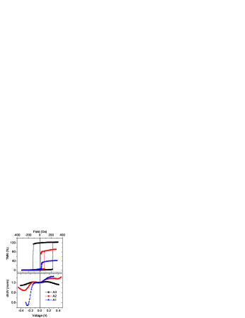
Figure 1a shows the TMR loops for samples A1-A3, with field applied along the in-plane easy axis of the MTJ. The TMR decreases with decreasing FL thickness due to reduced spin polarization of the tunneling electrons sun_dependence_1999 . Moreover, the magnetization of the FL is tilted out of the film plane due to the perpendicular interface anisotropy in thin CoFeB layer ikeda_perpendicular-anisotropy_2010 ; khalili_amiri_switching_2011 and therefore, at zero magnetic field a full parallel state for samples A1 and A2 is not achieved. The coercive field of about 100 Oe for sample A3 is reduced to zero for sample A1 wisniowski_effect_2008 . Differential conductance versus DC bias voltage was measured for all samples using lock-in technique. The results are presented in Fig. 1b. The asymmetry between the thin FL and the RL for samples A2 and A3 is observed in comparison with symmetric A3 sample. This asymmetry arises from a different band structures in the ferromagnetic electrodes oh_bias-voltage_2009 .
| Sample No. | FL thickness | TMR | Ic P AP |
|---|---|---|---|
| (nm) | (%) | mA | |
| A1 | 1.35 | 50 | -0.95 |
| A2 | 1.57 | 100 | -1.8 |
| A3 | 2.3 | 120 | -2.4 |
Ferromagnetic coupling between the RL and FL stabilizes the low resistance state of the MTJs at zero applied magnetic field skowronski_interlayer_2010 ; serrano-guisan_inductive_2011 . All samples exhibited clear current induced magnetization switching measured for relatively long current pulses of 10 ms. The absolute switching current value needed to change the MTJ state from a P to AP, measured with no magnetic field assistance, was found to decrease with FL thickness due to reduced saturation magnetization (volume) of the FL (Table 1). The sample spectra of A2 measured with no magnetic field applied are shown in Fig. 2. Existence of the perpendicular interface anisotropy in the FL results in non zero angle theta between FL and RL magnetizations in a low resistance state at zero magnetic field (Fig. 1) and therefore the STT precession is excited even at low DC bias. An increase of the negative DC current of the polarization that favor the AP state (electrons flowing from the FL to the RL) results in increased amplitude of the oscillations, that exceeds 10 nV/ at 1.5 GHz and -1.7 mA. Further increase of the negative current magnitude results in switching the MTJ to the high resistance AP state, where peak of much smaller amplitude and wider linewidth is observed.

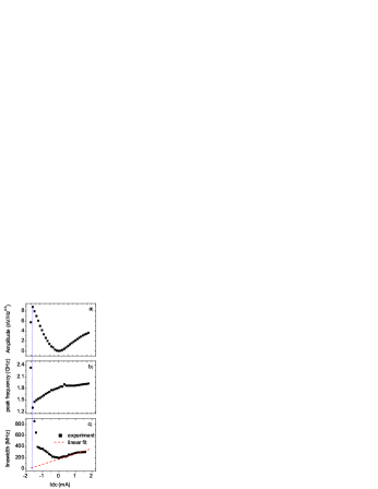
Fig. 3 presents the STO amplitude, peak frequency (f0) and linewidth f versus DC bias current with no magnetic field applied. Clearly, the oscillations for negative current favoring the AP state are more powerful than for the positive one, favoring P state, however peak at both current polarizations are visible due to a non zero angle theta at zero field. The dependence of linewidth of DC current is expressed as:
| (1) |
where is the spin polarization efficiency and Ic0 is the threshold current wada_spin-transfer-torque-induced_2010 . Extrapolating the f at the damping side (when MTJ is in P state and current favors P state) to zero Hz estimates the threshold current value (dotted line in Fig. 3. Moreover, a rapid change both in f0 and f is observed near the switching threshold. A similar current value was measured during the static CIMS experiment. The switching voltage is much smaller than the breakdown voltage, therefore we can induce steady state precession without destroying the MTJ.

The peak frequency at constant Idc = -1 mA and (Hdc) = 0 was found to increase with increasing FL thickness, results are presented in Fig. 4. Increased anisotropy constant results in smaller precession trajectories and therefore increased f0. It should be noted, that a sample-to-sample distribution in both oscillation’s amplitude and frequency is observed, mainly due to the size and shape distribution during a nano-lithography process, however the overall tendency is retained. For other samples with thinner FL of 1.22 nm we were not able to observe any oscillation in the measured bandwidth even with strong magnetic field applied in-plane of perpendicular to the sample’s easy axis. For sample A2 the oscillation’s amplitude is of the same order than the highest reported to date deac_bias-driven_2008 exceeding 10 nV/. We conclude, that taking advantage of the coupling mechanisms in MTJs with a thin MgO tunnel barrier in combination with perpendicular interface anisotropy might enhance STOs performance without the need of an external magnetic field application.
In summary we have demonstrated an STO based on an asymmetric MTJ, that is able to produce a microwave signal without a need of the magnetic field applications. Due to the ferromagnetic interlayer exchange coupling in our system, the MTJ is in stable low resistance state at Hdc = 0. Perpendicular interface anisotropy is thin FL is used, to induce the magnetization precession at small DC bias. The oscillation’s amplitude exceeds 10 nV/ at 1.5 GHz and Idc = -1.7 mA.
The authors would like to thank Singulus Technologies AG for consultation and technical help with MgO wedge MTJs preparation. Work supported by the SPINLAB POIG.02.02.00-00-020/09 project. T.S. and W.S. acknowledge Foundation for Polish Science MPD Programme co-financed by the EU European Regional Development Fund. and the Polish Ministry of Science and Higher Education grants (IP 2010037970 and NN 515544538). S.v.D. acknowledges financial support from the Academy of Finland for the ACTIVE-BAR project (no. 127731).
References
- [1] Yiming Huai, Frank Albert, Paul Nguyen, Mahendra Pakala, and Thierry Valet. Observation of spin-transfer switching in deep submicron-sized and low-resistance magnetic tunnel junctions. Applied Physics Letters, 84(16):3118, 2004.
- [2] Riichiro Takemura, Takayuki Kawahara, Katsuya Miura, Hiroyuki Yamamoto, Jun Hayakawa, Nozomu Matsuzaki, Kazuo Ono, Michihiko Yamanouchi, Kenchi Ito, Hiromasa Takahashi, Shoji Ikeda, Haruhiro Hasegawa, Hideyuki Matsuoka, and Hideo Ohno. A 32-Mb SPRAM with 2T1R memory cell, localized Bi-Directional write driver and ‘1’/‘0’ Dual-Array equalized reference scheme. IEEE Journal of Solid-State Circuits, 45(4):869–879, April 2010.
- [3] S. I. Kiselev, J. C. Sankey, I. N. Krivorotov, N. C. Emley, R. J. Schoelkopf, R. A. Buhrman, and D. C. Ralph. Microwave oscillations of a nanomagnet driven by a spin-polarized current. Nature, 425(6956):380–383, 2003.
- [4] W. Rippard, M. Pufall, S. Kaka, S. Russek, and T. Silva. Direct-Current induced dynamics in Co90Fe10/Ni80Fe20 point contacts. Physical Review Letters, 92(2), January 2004.
- [5] Alina M. Deac, Akio Fukushima, Hitoshi Kubota, Hiroki Maehara, Yoshishige Suzuki, Shinji Yuasa, Yoshinori Nagamine, Koji Tsunekawa, David D. Djayaprawira, and Naoki Watanabe. Bias-driven high-power microwave emission from MgO-based tunnel magnetoresistance devices. Nature Physics, 4(10):803–809, August 2008.
- [6] J. C. Slonczewski. Current-driven excitation of magnetic multilayers. Journal of Magnetism and Magnetic Materials, 159(1-2):L1–L7, 1996.
- [7] L. Berger. Emission of spin waves by a magnetic multilayer traversed by a current. Physical Review B, 54(13):9353–9358, 1996.
- [8] W. Skowronski, T. Stobiecki, J. Wrona, K. Rott, A. Thomas, G. Reiss, and S. van Dijken. Interlayer exchange coupling and current induced magnetization switching in magnetic tunnel junctions with MgO wedge barrier. Journal of Applied Physics, 107(9):093917, 2010.
- [9] J. Wrona, J. Langer, B. Ocker, W. Maass, J. Kanak, T. Stobiecki, and W. Powroźnik. Low resistance magnetic tunnel junctions with MgO wedge barrier. In Journal of Physics: Conference Series, volume 200, page 052032, 2010.
- [10] J. J. Sun and P. P. Freitas. Dependence of tunneling magnetoresistance on ferromagnetic electrode thickness and on the thickness of a cu layer inserted at the AlO/CoFe interface. Journal of applied physics, 85:5264, 1999.
- [11] S. Ikeda, K. Miura, H. Yamamoto, K. Mizunuma, H. D. Gan, M. Endo, S. Kanai, J. Hayakawa, F. Matsukura, and H. Ohno. A perpendicular-anisotropy CoFeB–MgO magnetic tunnel junction. Nature Materials, 9(9):721–724, July 2010.
- [12] P. Khalili Amiri, Z. M. Zeng, J. Langer, H. Zhao, G. Rowlands, Y.-J. Chen, I. N. Krivorotov, J.-P. Wang, H. W. Jiang, J. A. Katine, Y. Huai, K. Galatsis, and K. L. Wang. Switching current reduction using perpendicular anisotropy in CoFeB–MgO magnetic tunnel junctions. Applied Physics Letters, 98:112507, 2011.
- [13] P. Wiśniowski, J. M. Almeida, S. Cardoso, N. P. Barradas, and P. P. Freitas. Effect of free layer thickness and shape anisotropy on the transfer curves of MgO magnetic tunnel junctions. Journal of Applied Physics, 103(7):07A910, 2008.
- [14] Se-Chung Oh, Seung-Young Park, Aurélien Manchon, Mairbek Chshiev, Jae-Ho Han, Hyun-Woo Lee, Jang-Eun Lee, Kyung-Tae Nam, Younghun Jo, Yo-Chan Kong, Bernard Dieny, and Kyung-Jin Lee. Bias-voltage dependence of perpendicular spin-transfer torque in asymmetric MgO-based magnetic tunnel junctions. Nature Physics, 5(12):898–902, October 2009.
- [15] S. Serrano-Guisan, W. Skowronski, J. Wrona, N. Liebing, M. Czapkiewicz, T. Stobiecki, G. Reiss, and H. W Schumacher. Inductive determination of the optimum tunnel barrier thickness in magnetic tunnelling junction stacks for spin torque memory applications. Journal of Applied Physics, 110(2):023906, 2011.
- [16] T. Wada, T. Yamane, T. Seki, T. Nozaki, Y. Suzuki, H. Kubota, A. Fukushima, S. Yuasa, H. Maehara, Y. Nagamine, K. Tsunekawa, D. D. Djayaprawira, and N. Watanabe. Spin-transfer-torque-induced rf oscillations in CoFeB/MgO/CoFeB magnetic tunnel junctions under a perpendicular magnetic field. Physical Review B, 81(10), March 2010.