Bilayer graphene dual-gate nanodevice: An ab initio simulation
Abstract
We study the electronic transport properties of a dual-gated bilayer graphene nanodevice via first principles calculations. We investigate the electric current as a function of gate length and temperature. Under the action of an external electrical field we show that even for gate lengths up Å, a non zero current is exhibited. The results can be explained by the presence of a tunneling regime due the remanescent states in the gap. We also discuss the conditions to reach the charge neutrality point in a system free of defects and extrinsic carrier doping.
pacs:
72.80.Vp,85.30.Tv,73.23.Ad,71.15.MbThere is a consensus in the scientific community that the scaling down of silicon-based metal-oxide-semiconductor field-effect transistors (MOSFETs) is approaching its limits. Therefore, there is a pursuit for different materials to replace the silicon paradigmgr-trans . Among the potential candidates, graphene has attracted the attention of research groups after the seminal work of the Manchester groupgraph-first . Graphene is a truly two-dimensional (2D) material, with a honeycomb structure, and is a zero band-gap semiconductor. The valence and conduction bands close to the Fermi level are cone shaped, with a linear energy-momentum relation at the two points ( and ) of the Brillouin zone, called Dirac pointscastro_RMP . As a result, graphene has several properties that make it very interesting to use in the manufacture of devices, such as its very high electronic mobilities, up to mobility1 ; mobility2 , with electrons and holes behaving as massless fermions near the and points. Thus, charge carriers can travel for micrometers at room temperature without any scattering.
However, a drawback in using graphene as an electronic material, such as in logic devices, is its lack of an energy gap. A number of different approaches have been proposed to open such a bandgap on graphenegap-gr1 ; gap-gr2 ; gap-gr3 ; gap-gr4 ; gap-gr5 . Another way to create the gap is to use bilayer graphene, breaking the inversion symmetry through an external perturbation, such as the application of an electrical field perpendicular to the layers. Moreover, this band gap can be tuned by varying the field strength. This fact has been confirmed by both photoemission and optical absorption experimentstunable1 ; tunable2 ; tunable3 . A few theoretical studies have also investigated this approach to open a band gap in bilayer graphene via the application of an electric field along the whole systemteo-gap-bl1 ; teo-gap-bl2 . Recently, Avouris’ group observed a transport band gap in biased bilayer grapheneon-off , also demonstrating its potential for applications in digital electronics. Thus, understanding the intrinsic properties of devices based on bilayer graphene in nano-dimensions is important for future developments in the area.
In this Brief Report we present investigations of the electronic transport properties of a dual-gated bilayer graphene nanodevice, as a function of the gate length () and temperature, via first-principles calculations. We show an exponential decrease of the current as a function of the gate length, which is characteristic of a tunneling regime. As a result, the system does not reach a zero current. Also, we discuss the conditions to achieve the charge neutrality point (CNP) in a system that is not affected by defects and extrinsic carrier doping. We present results for electric fields comparable to the experimental electric displacement fields, , for room temperature and . We use the Landauer-Büttiker model, with a Hamiltonian generated through ab initio density functional theory (DFT),dft1 coupled with a non equilibrium Green’s function formalism in a fully self-consistent procedure (NEGF-DFT)negf1 . To investigate the effect of finite gates we implement a real-space Poisson solver with multigrid techniquesmult1 .
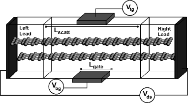
In Fig. 1 we show a schematic representation of the bilayer dual-gated graphene nanotransistor considered in our calculations. The atomic geometry is composed of an stacked bilayer graphene (BG) with a scattering region up to nm in length, sandwiched by left and right leads. A source-drain voltage () is applied across the system defining the current direction. The charge transport properties were calculated with the NEGF-DFT formalism, which uses the Kohn-Sham Hamiltonian and overlap matrices computed with the siesta codesiesta to self-consistently obtain the density matrix. In order to investigate a finite dual-gate system, we have done two main modifications in the transampa code transampa : (i) The inclusion of points that are transversal to the transport direction (), where for each point in reciprocal space we find a -dependent density , by means of an integration of the lesser Green’s functiondft_negf ; ref39 , and transmittance , given by:negf4
| (1) |
is the retarded (advanced) Green’s function, whereas, are the terms that couple the leads to the scattering region. The total density and transmittance are obtained upon an integration in the reciprocal space with the following equations:
| (2) |
| (3) |
These modifications allow the simulations of truly 2D systems. Once the density matrix convergence is achieved, the current is calculated within the Landauer-Büttikernegf1 model in the non-interacting approach of Meir-Wingreennegf4 , where the current is given by:
| (4) |
is given by (3), and are the Fermi-Dirac distributions for the left(L)/right(R) leads. We used the local density approximation (LDA) for the exchange-correlation functionalpz since it correctly describes the graphene interlayer distance without the inclusion of van der Waals corrections.vdw (ii) The second modification was the inclusion of a real-space Poisson solver that allows non-periodic solutions for the Hartree potential, necessary to set different values for the top () and back () gate voltages with finite gate lengths. Therefore, we solve the Poisson equation in a rectangular box, fixing the upper and lower boundary conditions, where the values of and are defined only in a finite region of length (see Fig. 1). In our investigation we consider , and , , and a distance between the upper and lower boundaries of Å.
We guarantee the convergence of the transmittance using a double- basis, for the mesh cut-off and 800 points in the Brillouin zone with the Monkhorst-Pack schememonkhost . We used a fully relaxed geometry with a carbon-carbon distance of Å and an interlayer distance of Å. In the transport calculations, a tiny imaginary value of is added to the energy in order to calculate the retarded Green’s function, and the electron density was calculated with 60 energy points and 5 poles to evaluate the integral of the lesser Green’s function.
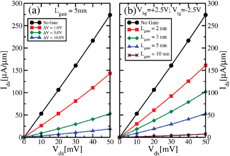
The flowing current as a function of the source-drain voltage is depicted in Figs. 2(a) and 2(b) for room temperature. In our simulations the gate voltages and are tuned independently. In Fig. 2 all curves are for gate voltages with , where the voltage difference is . In Fig. 2(a) we used , and , generating electric fields of , , and , comparable to experimental values. In all experimentson-off ; tunable2 ; prl_105_166601 , the electric displacement field in the bilayer is estimated through the dielectric constant and thickness of the substrate dielectric layer, and from the effective potential caused by the carrier doping due to the experimental conditions. In this Brief Report, the electric field was calculated via , where is the distance between the bottom and top gates. For the configuration studied here, we verify a decrease of the current as increases, suggesting the opening of a band gap that increases with . Moreover, for fixed gate length and gate voltages, the electric current has a linear dependence with the source-drain voltage, indicating an ohmic contact between the gated and non-gated bilayer graphene. This behavior is also observed experimentallyon-off ; tunable1 ; tunable2 ; tunable3 . From Fig. 2(a) we show that we do not reach a zero electric current, even for . This result is in agreement with experimental works that fabricate dual-gate bilayer graphene deviceson-off .
In Fig. 2(b) we fixed the and , and we present the dependence of the flowing current with the gate length , for , up to . We also observe a decrease of the current as increases, indicating an increase of the region with a gap. Again, the system does not reach a zero current even for .
Since we used open-boundary conditions, with the chemical potential fixed by the leads, we can independently vary and to control the carriers at the scattering region. The presence of the external electric field causes a breakdown of the equivalence between the two layers. As a result, there is the opening of a band gap and an inter-layer charge transfer. If there were no charge transfer, the condition would define the charge neutrality point (CNP). However, the presence of a Hubbard-like correlation termtb-matheus , even at the mean-field level, coupled to this charge transfer, leads to an overall shift of the bands. As a result, the CNP occurs for , as shown in Fig. 3.

Thus, we performed calculations where we fixed the at a certain value (+2.5 V) and varied the . The calculated source-drain current and net carrier concentration in the bilayer, as a function of the top gate, is shown in Figs. 3(a) and 3(b) for a gate length , for and , respectively. The bias voltage was fixed at . The current minimum in both curves corresponds to the charge neutrality point. For a top gate voltage higher than , electrons are being injected in the scattering region, whereas for below this value the holes are being injected. As we have no external doping, the chemical potential at the gated graphene is at the midgap. Moreover, since the conduction and valence bands are very similar, temperature will create intrinsic carriers but it will not change the position of the chemical potential. Thus, there will be some charge transfer from the graphene leads (electrons or holes) depending on the shift of the mid-gap position, at the gated graphene region, relative to the chemical potential of the leads. Also, in Figs. 3(a) and 3(b) we plot the carrier concentration per unit area. This presents a linear behavior as a function of the variation of the gate voltage, with zero net charge at the charge neutrality point. This indicates a linear displacement of the bands with the gate voltage. There is a notable decrease in the current when the temperature is diminished from to . This is caused both by variations in the transmittance with temperature as well as by changes in the tail of the Fermi-Dirac distribution [see Eq. (4)]. For the case presented in Fig. 3, the current decreases by more than six times. However, the net charge concentration is very similar in both temperatures, a result of the invariance of the mid-gap position with temperature, as discussed above.
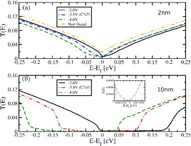
Figure 4 shows the effect of the gate potential in the transmittance for (a) and (b) ; at with a fixed back gate voltage of , and varying . Under the same conditions, for larger gates the modifications on the transmittance are more expressive in comparison to the smaller ones. For each configuration the gate potentials causes a low transmittance region that is much more pronounced with in comparisson with . However, the transmittance never goes to zero, as can be seen on the inset in Fig. 4(b).
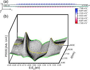
It is important to emphasize that in our calculations the electric field is applied only in a finite portion of the scattering region through the dual-gate system. As a consequence, the inter-layer charge transfer caused by this electric field occurs only in the gated region. In Fig. 5(a) we present the charge induced at CNP, by a dual gate with . In the bottom (top) layer there is an excess (lack) of electrons. In Fig. 5(b) we show the density of states projected on every four atoms (equivalent to the unitary cell) along its entire length, from the left-hand () to the right-hand electrodes (). Near to the leads (green lines) the projected density of states (PDOS) are similar to the PDOS of a non-gated pristine bilayer, as expected, whereas directly under the gated region (yellow line) the PDOS is characteristic of a bilayer with an applied perpendicular electric field, where the two peaks located at approximately are associated with the presence of a ”mexican” hat behavior of the bands. However, since the gate is spatially finite, even in the presence of an energy band gap there is a finite density of states present. This is due to the penetration of the wave function in this forbidden energy region. This results explains the absence of an energy gap for transport [e.g.. see Fig. 4(b).]
To understand further the persistent current on the device, we look at its behavior as a function of the gate length. In Fig. 6, we fix and , and vary for and . We obtain an exponential dependence between the current and the gate length, characteristic of a tunneling regime. The tunneling current persists even for the largest gate length, . A significant increase of the current with temperature can be observed; this is largely caused by the broadening of the transport window via the term. At the low-bias regime, the tail of the Fermi-Dirac function mostly controls the current, since there is a small density of states (and hence a small number of transport channels) around the Fermi level in the electrodes. It is important to remind that in our ab initio calculations we retain all the intrinsic properties of the device, without the presence of defects, impurity carrier doping, or a substrate dielectric material. Therefore, the off-current in our simulations is explained by tunneling across the gated region, and strongly depends on the transport energy window caused by the Fermi-Dirac distribution.
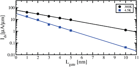
For our nanodevice we estimated the on/off current ratio, at room temperature, , and low temperature, . The on current is calculated for the non-gated bilayer graphene with a source-drain voltage of and the off currents are all defined at the charge neutrality point, with a back gate voltage of and the source-drain voltage fixed at . The largest happens at , which is around at room temperature, and at .
In summary, using ab initio calculations, we study the electronic transport properties of a dual-gated bilayer graphene nanotransistor. Under the action of an external electric field, we show that, even for gate lengths up to Å and for room temperature and , a non-zero current is exhibited. The results can be explained by the presence of a tunneling regime due the remanescent states in the gated region.
We would like to thank E. Mucciolo for comments and discussions. This research was supported by Brazilian agencies INCT/CNPq and FAPESP.
References
- (1) F. Schwierz, Nature Nanotechnol. 5, 487 (2010).
- (2) K. S. Novoselov et al., Science 306, 666 (2004).
- (3) A. H. Castro Neto et al., Rev. Mod. Phys. 81, 109 (2009).
- (4) X. Du et al., Nature Nanotechnol. 3, 491 (2008);
- (5) K.I. Bolotin et al. Sol. State Comm. 146, 351 (2008).
- (6) M. P. Lima, A. R. Rocha, A. J. R. da Silva, A. Fazzio, Phys. Rev. B 82, 153402 (2010)
- (7) M. Y. Han, J. C. Brant, and P. Kim, Phys. Rev. Lett. 104 056801 (2010);
- (8) K. F. Mak, C. H. Lui, J. Shan and T. F. Heinz, Phys. Rev. Lett. 102, 256405 (2009);
- (9) Z. H. Ni et al., ACS Nano 2, 2301 (2008).
- (10) X. Wang et al., Phys. Rev. Lett. 100, 206803 (2008).
- (11) J. B. Oostinga, H. B. Heersche, X. Liu, A. F. Morpurgo and L. M. K. Vandersypen, Nature Mat. 7, 151 (2007);
- (12) Y. Zhang et al., Nature (London) 459, 820 (2009).
- (13) K. F. Mak, C. H. Lui, J. Shan and T. F. Heinz, Phys. Rev. Lett. 102, 256405 (2009)
- (14) H. K. Min, B. Sahu, S. K. Banerjee, A. H. MacDonald, Phys. Rev. B 75, 155115 (2007).
- (15) E. McCann, Phys. Rev. B 74, 161403(R) (2006).
- (16) F. Xia, D. B. Farmer, Y.-M. Lin and P. Avouris, Nano Lett. 10, 715 (2010)
- (17) P. Hohenberg, W. Kohn ,Phys. Rev. 136, B864 (1964); W. Kohn and L.J. Sham, Phys. Rev. 140, A1133 (1965); K. Capelle, Braz. J. Phys. 36, 1318 (2006).
- (18) R. Landauer, Philos. Mag. 21, 863 (1970); M. Büttiker, Y. Imry, R. Landauer, and S. Pinhas, Phys. Rev. B 31, 6207 (1985); M. Büttiker, Phys. Rev. Lett. 57, 1761 (1986);
- (19) M. P. Merrick, K. A. Iyer and T. L. Beck, J. Phys. Chem. 99, 12478 (1995).
- (20) E. Artacho et al., Phys. Status Solidi B 215, 809 (1999).
- (21) F. D. Novaes, A. J. R. da Silva and A. Fazzio, Braz. J. Phys. 36, 799 (2006); J. E. Padilha, R. B. Pontes, A. J. R. da Silva and A. Fazzio, Int. J. Quantum Chem. n/a, doi: 10.1002/qua.22690
- (22) M. Brandbyge, J.-L. Mozos, P. Ordejón, J. Taylor, and K. Stokbro, Phys. Rev. B 65, 165401 (2002).
- (23) H. Haug and A.-P. Jauho, Quantum Kinetics in Transport and Optics of Semiconductors (Springer-Verlag, Berlin, 1996).
- (24) Y. Meir and N. S. Wingreen, Phys. Rev. Lett. 68, 2512 (1992).
- (25) J. P. Perdew and A. Zunger, Phys. Rev. B 23, 5048 (1981).
- (26) M. P. Lima, A. Fazzio, A. J. R. da Silva, Phys. Rev. B 79, 153401 (2009).
- (27) H. J. Monkhorst and J. D. Pack , Phys. Rev. B 13, 5188 (1976).
- (28) T. Taychatanapat and P. Jarillo-Herrero, Phys. Rev. Lett. 105, 166601 (2010).
- (29) M. P. Lima, A. J. R. da Silva and A. Fazzio, Phys. Rev. B 81, 045430 (2010).