Dielectric capping effects on binary and ternary topological insulator surface states
Abstract
Using a density functional based electronic structure method, we study the effect of crystalline dielectrics on the metallic surface states of Bismuth- and chalcogen-based binary and ternary three dimensional topological insulator (TI) thin films. Crystalline quartz (SiO2) and boron nitride (BN) dielectrics were considered. Crystalline approximation to the amorphous quartz allows to study the effect of oxygen coverage or environmental effects on the surface states degradation which has gained attention recently in the experimental community. We considered both symmetric and asymmetric dielectric cappings to the sufaces of TI thin films. Our studies suggest that BN and quartz cappings have negligible effects on the Dirac cone surface states of both binary and ternary TIs, except in the case of an oxygen-terminated quartz surface. Dangling bond states of oxygens in oxygen-terminated quartz dominate the region close to Fermi level, thereby distorting the TI Dirac cone feature and burying the Dirac point in the quartz valence band region. Passivating the oxygen-terminated surface with atomic hydrogen removes these dangling bond states from the Fermi surface region, and consequently the clear Dirac cone is recovered. Our results are consistent with recent experimental studies of TI surface degradation in the presence of oxygen coverage.
pacs:
71.15.Dx, 71.18.+y, 73.20.At, 73.61.LeI Introduction
Three dimensional (3D) topological band insulator (TI) Bi2X3 (X=Se, Te) and its ternary counterparts have attracted considerable attention from the condensed matter physics community because of the relatively simple crystal structure that hosts novel surface stateszhang1 ; zahid1 . and their unusual responses to external fields. Many more 3D TI materials have been predictednew3d1 ; new3d2 ; new3d3 ; new3d4 ; new3d5 by now, and quest for studying their novel surface state properties, in isolation as well as in presence of other materials, has increased in recent years. The 3D TI surface states are time-reversal symmetric (TRS) at high-symmetry points in the momentum space and are therefore protected against perturbations which cannot break TRS such as non-magnetic impurities or adatoms. Such novel properties have caused excitement in the electron device community as well because it can be a potential alternative to graphene as a channel material in field effect transistors. The advances in understanding of structural, electronic, magnetic and transport properties of 3D TI, made possible by both experimental and theoretical studieszhang2 ; Burkov ; Hor , can provide important informations for novel applications. Beside the fundamental studies of these model 3D TI materials, theoretically, no studies of dielectric effects on the surface states have been performed so far from first principles. We address dielectric effects on the TI surface states using ab-initio density functional theory (DFT) and semi-local density approximationperdew . Two crystalline dielectrics were considered: quartz (SiO2) and boron nitride (BN). Both binary TI Bi2Se3 and ternary TIs Bi2Se2Te and Bi2Te2Se were considered for this study. Our studies suggest that neither of the two dielectrics has an effect on the Dirac cone except the oxygen-terminated quartz. Under the environment of oxygen dangling bond, the Dirac cone on the TI surface is buried inside the quartz valence band continuum with the oxygen dangling bond states occupying the region around the Fermi level. Surface passivation by atomic hydrogen pushes the dangling bond states from the Fermi surface region down below Fermi level and a clear Dirac cone emerges at the Fermi level. These findings are consistent with recent experimental studies of surface degradation effects in the presence of oxygenshen .
We begin by describing the thin film structures of both binary and ternary TIs, built from their bulk hexagonal structures, and the computational method in section II. In section III, we present the dielectric capping effects, by BN and SiO2, on their metallic surface states. Both symmetric and asymmetric cappings are explored. Finally we present our summary and conclusions.
II Isolated Thin Films and Computational Approach
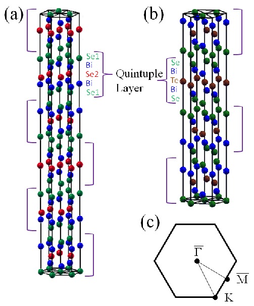
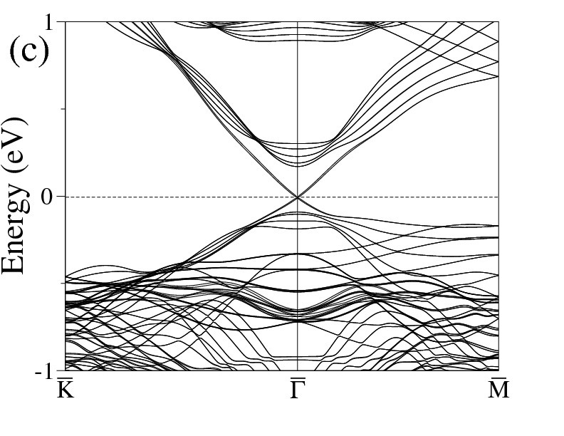
The thin film structures for both binary and ternary TIs are constructed by stacking up several quintuple layers (or QLs: 1QL=5 atomic layers) along the crystallographic z-direction with a vacuum region of 3 nm which forms the supercell in the DFT calculation. The first principle calculations were performed using the OPENMX codeOpenmx1 , based on a linear combination of pseudoatomic orbital (PAO) methodOpenmx2 . The pseudopotentials were generated from full relativistic calculations, and the generalized gradient approximationperdew was applied for the exchange-correlation potential. The kinetic energy cut-off of 180 Rydberg and the k-point mesh of 7 7 1 for Brillouin zone (BZ) integration (Fig. 1(c)) were used. The basis sets were carefully chosen to reproduce previous bulk and thin film calculations. The cut-off, k-point mesh and vacuum region were optimized to guarantee the convergence of the results and their agreement with previous theoretical calculations.
For the binary TI, previous theoretical studies of bulk Bi2Se3 found the computed lattice parameters close to the experimental valueszhang2 , so we used the experimental lattice parameters a=0.41388 nm and c=2.8633 nm in the hexagonal unit cell and optimized bulk atomic positions to build the thin film structure. For the ternary TI Bi2Se2Te (Bi2Te2Se), we built thin film structures with the bulk hexagonal unit cell lattice parameters a=0.422 nm (0.428 nm) and c=2.92 nm (2.99 nm) in the previous theoretical calculationjiwon , and optimized the thin film structure by letting atoms move along z-direction. We optimized thin film structures only for ternary TIs, since atomic relaxations significantly affect the band structure of thin film Bi2Se2Te around the Dirac pointjiwon . We considered the thin film of 6QLs and 4QLs for binary and ternary TIs, respectively, since previous studies on binaryliu ; zhang3 and ternaryjiwon TIs suggest that 6QLs and 4QLs are the minimum thicknesses to maintain the gapless surface state at the Dirac point. We also obtained the same critical thickness values by our own calculations. In the calculated band structure of 6QLs Bi2Se3, we could observe the Dirac cone within a bulk gap of 0.262 eV. For the ternary TIs Bi2Se2Te and Bi2Te2Se, Dirac cone surface states reside inside the bulk gap of 0.204 eV and 0.325 eV, respectively.
III Thin Films with Symmetric and Asymmetric Dielectric Cappings
We chose crystalline SiO2 in order to assess the effect of oxygen environment on the TI surface states. The choice of BN dielectrics is perhaps guided by the recent graphene transport experiments using crystalline dielectricsphilip1 ; philip2 . We considered both symmetric and asymmetric cappings in terms of relative orientations of TI and dielectric surface atoms. Asymmetry in terms of different dielectrics on two opposite TI surfaces was not considered.
The bulk structures of both dielectrics were studied with the computational parameters described in the previous section. For the hexagonal BN, the experimental lattice paramters are: a=0.2494 nm and c=0.666 nm with the distance between B and N dB-N=0.144 nmCrystalBN , and the band gap is 5.97 eVkanda . We used the experimental values of lattice constants and atomic positions. With these experimental values, our calculated bulk band gap value is 5.5 eV close to the experimental value 5.97 eV. The hexagonal crystal structure of quartz contains fourfold coordinated oxygens, forming a layered structure with Si with the experimental lattice parameters (a=0.4914 nm and c=0.5408 nmquartz ). Our DFT calculations of optimized lattice paramters with semi-local potentials are found to be close to these experimental values, accurate to within 0.1. Therefore, we chose experimental lattice parameters for building our interface structures of TI and quartz. The bulk quartz SiO2 has a direct band gap of 9 eVsio2gap , and our DFT calculation of crystalline SiO2 results in a band gap value of 9.4 eV. We note that our results obtained for quartz should be considered at best qualitative with regard to TIs capped with amorphous SiO2.
III.1 Thin Films of Binary TI Bi2Se3 with Dielectrics
In this section, we discuss the thin film of binary TI Bi2Se3.
III.1.1 Construction of Supercell Structure
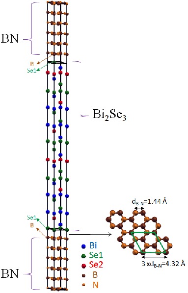
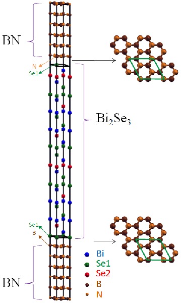
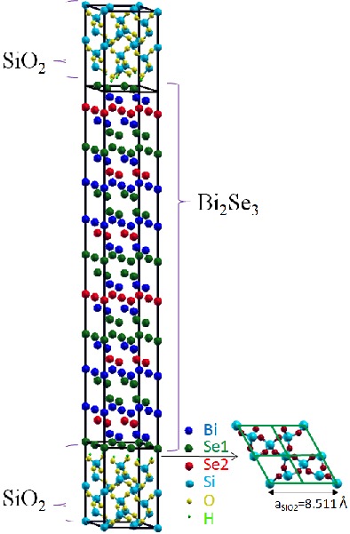
The interface structures are built by putting the dielectric material on the surfaces of 6QLs of Bi2Se3 film stacked along the z-direction (since it has no band gap for the surface states). In constructing supercells, we maintained the TI lattice and strained the dielectrics to fit with the TI surface resulting in the compressive or tensile strain on the dielectrics to focus on their effects on the TI electronic structure. For the BN, our analysis suggests that to keep our computational burden in DFT-based calculations minimal, 3dB-N3dB-N lattice structure can be matched in-plane with 11 Bi2Se3 cell (Fig.2 and Fig.3) or any multiples of this combination which maintains 3:1 matching ratio resulting in the 4.19 compressive strain on BN (in Table I). Other combinations to allow less strain result in either difficulty in forming the periodic structure or larger supercells with orders of magnitude more atoms. Along the stacking direction, 6QLs of Bi2Se3 (6nm) is put on six atomic layers of BN (1.7nm). The choice of 6 BN layers is somewhat arbitrary and guided by the fact that the size of vacuum and BN layers should be thick enough to avoid interactions of periodically repeated Bi2Se3 surface layers. We also relaxed the interfacial atoms to assess its effects. For the SiO2 dielectric, the supercell structure consists of two unit cells of SiO2 sandwiching 6QLs Bi2Se3. The size of SiO2 and Bi2Se3 cell along x-y direction chosen is, respectively, 11 and 22 (Fig. 4) to minimize the computational cost. This produces about 2.75 compressive strain on both sides of SiO2 as in Table I. Consideration of larger sizes can lead to the lower strain, but the total number of atoms in the cell increases at least an order of magnitude (250 versus 2500).
We considered four configurations of Se positions on the TI surfaces with respect to boron and nitrogen positions on the BN layer: Se on the top of B, on the top of N, on the hexagonal hole and on the bond between B and N atoms. Two surface terminations, Si and oxygen, of quartz were considered. Our calculations suggests that all BN configurations are energetically close and provide quite similar band structures. Therefore, we had a choice in the selection of a particular configuration for further studies. We chose the case of B or N on the top of Se on both TI surfaces. We refer the structure of B or N on the top of Se on both sides of TI film as symmetric capping (Fig. 2). The structures of B on the top of Se on one side and N on the top of Se on the other side of TI film, or only B or N on one side of TI film and vacuum on the other side, are referred as asymmetric capping (Fig. 3). For quartz, both TI surfaces capped with either oxygen-terminated or Si-terminated quartz were considered. Because quartz is a fourfold coordinated structure, both of the surface terminations of quartz possess dangling bonds. Therefore, for quartz we also considered the dangling bond saturation with hydrogen, that is, hydrogen passivation of the quartz surfaces.
To set the optimal distance between the BN and Bi2Se3 layers at the interface, we performed the total energy calculations at the chosen set of interfacial distances. Our studies suggest an optimal distance of 0.3 nm for the case of the Se layer in Bi2Se3 on the top of either B or N in BN. For Bi2Se3 on quartz, the interfacial distances for Si and oxygen quartz terminations with and without hydrogen passivation need to be considered. Our studies suggest an optimal distance of 0.3 nm for Si-terminated surface, regardless of whether dangling bonds are saturated or not. For the oxygen-terminated quartz with hydrogen passivation, we found the optimal distance to be 0.25 nm. We considered these optimal interfacial distances in our further studies.
We considered the atomic relaxation in the interfacial region in order to check its effect on the electronic structure of TI surface states. Two cases were considered: first is the case of Se on the top of B atom on both sides of TI with the initial optimal separation of 0.3 nm. We let atoms close to the interface (Bi/Se atoms in the top and bottom QLs and B/N atoms in the two layers next to TI surfaces) move in the z-direction. The second choice is that the oxygen-terminated quartz with the saturation of dangling bonds is put on both TI surfaces with optimal separation of 0.25 nm. Bi/Se atoms in the top and bottom QLs as well as Si/O atoms next to the TI surfaces are allowed to move in the z-direction, while hydrogen atoms used to saturate dangling bonds are relaxed in all directions.
| TI | a (nm) | Strain on SiO2 | Strain on BN |
|---|---|---|---|
| Bi2Se3 | 0.41388 | 2.75 compressive | 4.19 compressive |
III.1.2 Results and Discussion
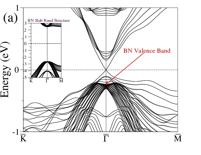
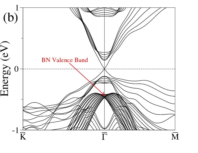
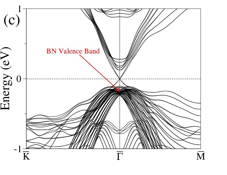
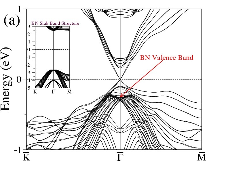
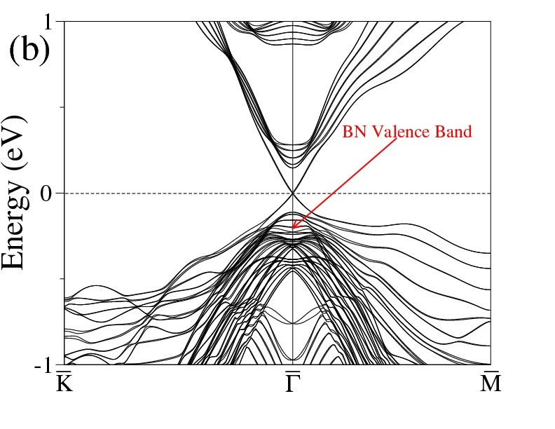
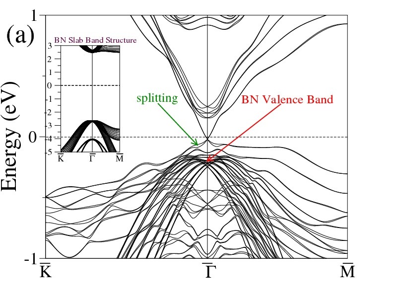
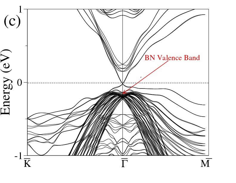
We first discuss the BN interface effects followed by the effects due to quartz surface terminations. Figs. 5(a) and (b), respectively, show the band structures of 6QLs Bi2Se3 capped on both sides by BN with either B on the top of Se atom or N on the top of Se atom (symmetric capping). The atomic relaxation is not considered here. The Dirac cone and its degeneracy are protected in both cases. This insensitivity of the Dirac cone to the presence of dielectric hints at negligible interactions between B or N orbitals with Se orbitals. We confirm this hypothesis by plotting atom-projected DOS in the same energy range as the band structures in Figs. 6(a) and 6(b). These plots show that both B and N orbitals are not in resonance with the Se orbitals of TI. As a result, the Dirac cone surface states are protected. From the band structure of only BN atomic layers without Bi2Se3 (inset in Fig. 5(a)) and the atom-projected DOS plots of Figs. 6(a) and 6(b), the BN valence band maximum is estimated to be about 0.25 eV and 0.45 eV below the Dirac point for B on the top of Se atom and N on the top of Se atom cases, respectively. The band structure including the effect of atomic relaxation for the structure of B on the top of Se on both sides is shown in Fig. 5(c). Comparison Fig. 5(c) with Fig. 5(a) indicates that the relaxation of interfacial atomic positions does not affect the essential characteristics of surface states near the Fermi surface. Fourfold degeneracy at the Dirac point and the dispersion relation still remain same, while valence bands of BN are a bit shifted close to the Dirac point. The bulk band gap size for each case (0.259 eV for B on the top of Se, 0.258 eV for N on the top of Se) does not change much from that of only 6QLs Bi2Se3 (0.262 eV).
In case of asymmetric capping, B on the top of Se atom on one side and vacuum on the other side of the TI film shows that the Dirac point degeneracy is still unaffected in Fig. 7(a). However, there is some splitting of valence and conduction bands close to it. With B on the top of Se on one side and N on the top of Se on the other side, the Dirac cone is not influenced either as seen in Fig. 7(b). Again, the atom-projected DOS plots in Figs. 8(a) and 8(b) suggest that this insensitivity is due to non-overlap of B and N orbitals with the Se orbitals. The position of BN valence band maximum is about 0.25 eV below the Fermi level for both cases similarly in the symmetric capping both TI surfaces with B on the Se, since B is placed on Se on one side of TI in both asymmetric cappings. The buulk band gap sizes are 0.268 eV and 0.257 eV for ’B on the top of Se atom on one side and vacuum on the other side’ and ’B on the top of Se on one side and N on the top of Se on the other side’, respectively.
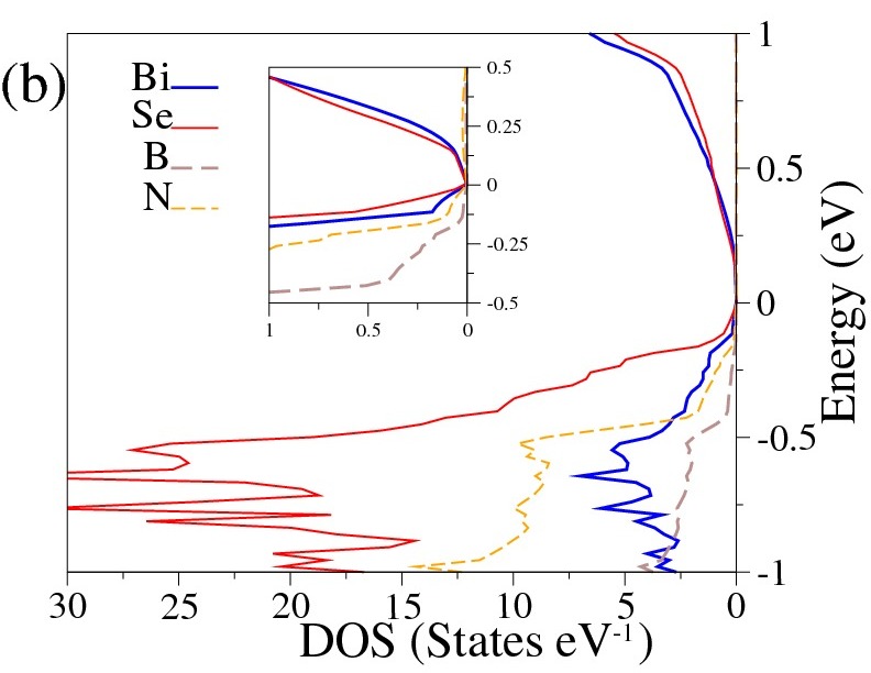
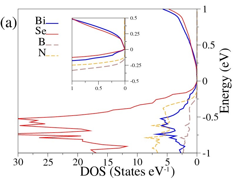
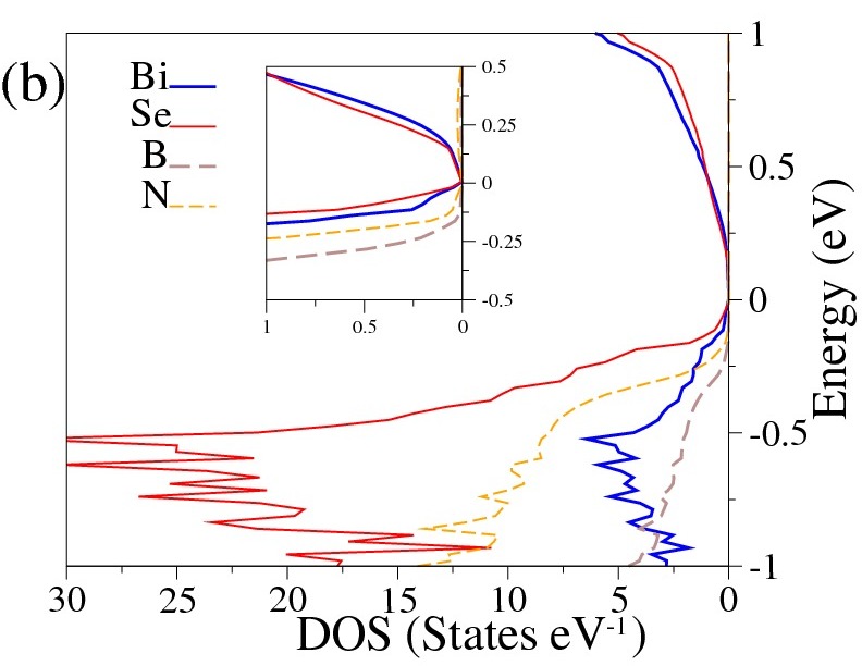
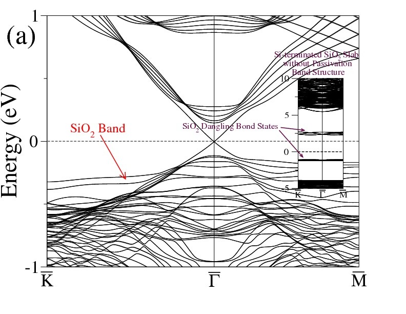
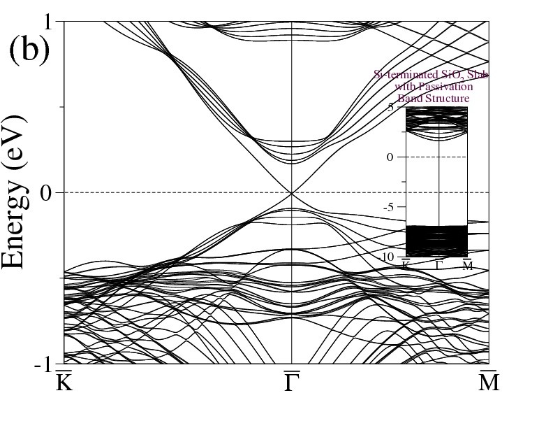
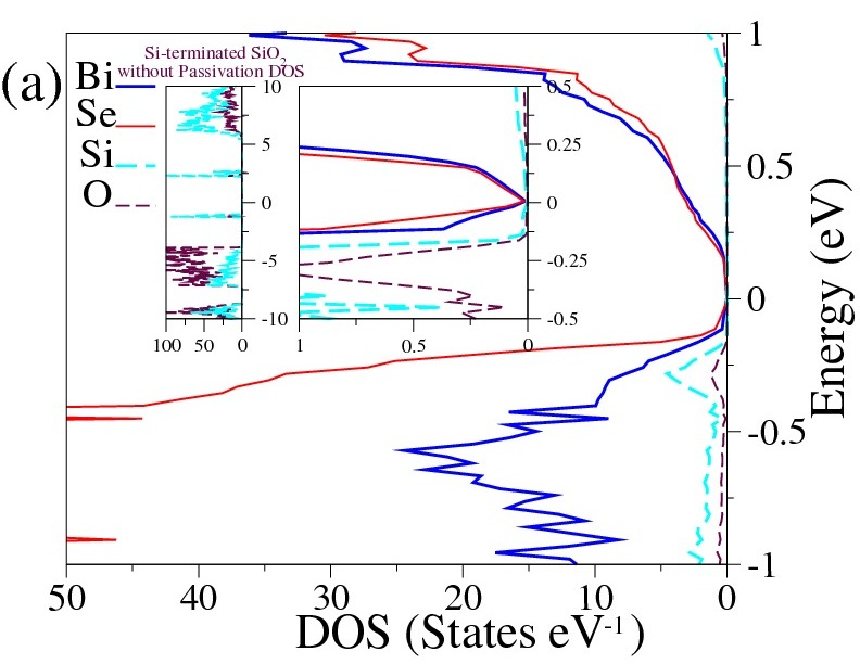
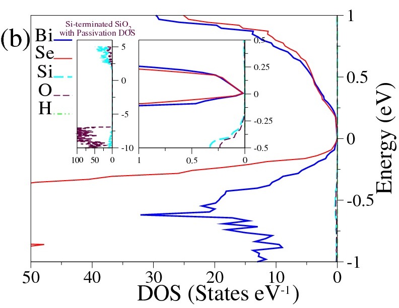
For Si-terminated SiO2, both without and with dangling bond passivations show the protected Dirac cone surface state (Figs. 9(a) and 9(b)), consistent with the DOS plots in Figs. 10(a) and 10(b). Si orbitals do not mix with Se orbitals in the energy range close to the Dirac point. The band structure of only Si-terminated quartz slab without the passivation (inset of Fig. 9(a)) and its DOS plot (left inset of Fig. 10(a)) show the Si dangling bond states within the bulk quartz band gap. These dangling bond states are also observed around the energy level of -0.26 meV in the band structure of Si-terminated quartz with Bi2Se3 (Fig. 9(a)), which is confirmed by the peak value of DOS from Si orbitals at -0.26 eV in Fig. 10(a). By the hydrogen passivation, dangling bond states are removed in the band gap of only Si-terminated SiO2 Slab as seen in the inset of Fig. 9(b) and the left inset of Fig. 10(b). As a result, we cannot find the SiO2 states in the energy range of -11 eV in Figs. 9(b) and 10(b).
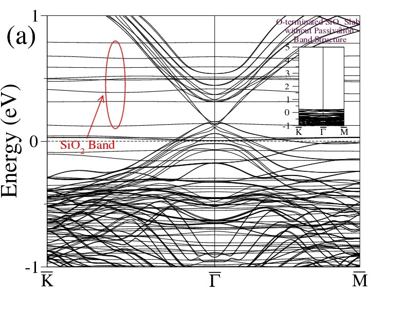
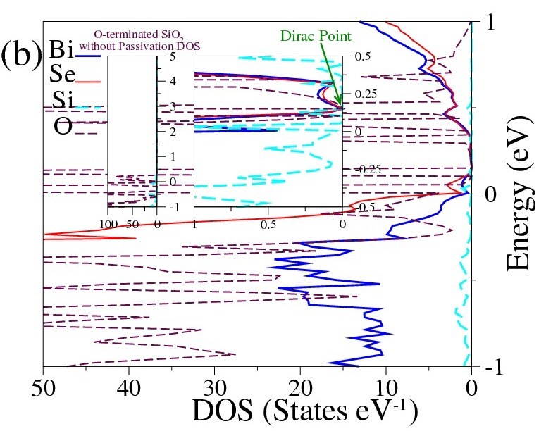
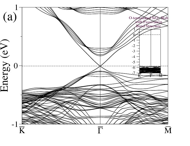
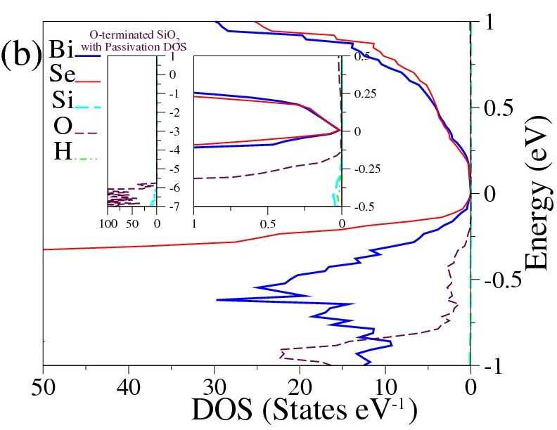
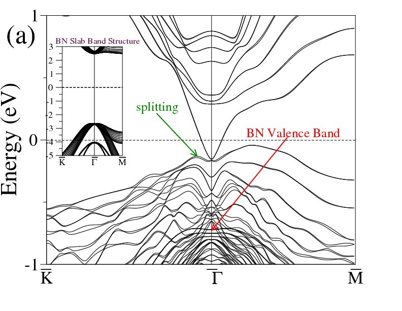
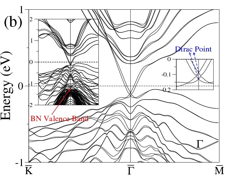
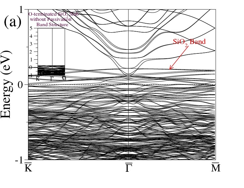
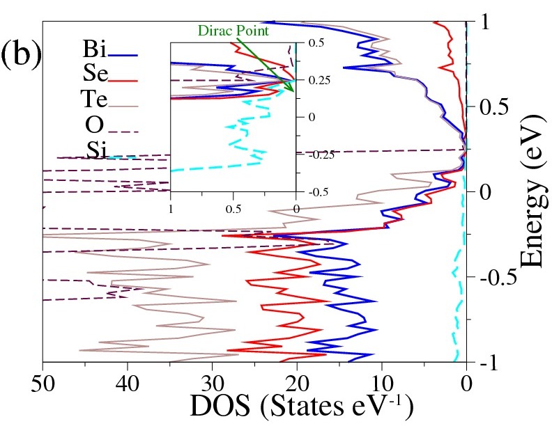
Fig. 11(a) is the band structure of the TI surface in the presence of oxygen-terminated quartz without passivation. The DOS plot (Fig. 11(b)) shows that oxygen orbitals lie close to the Se orbitals and dominate the region around Fermi level. By the effect of oxygen orbitals, the Dirac cone feature is significantly distorted. However, the Dirac point still remains intact, which can be confirmed by the linear increase of Bi and Se DOS around 0.15 eV in the right inset of Fig. 11(b). It exists close to the Fermi level and is buried inside SiO2 valence band continuum as shown in Figs. 11(a) and 11(b). In the band structure of only oxygen-terminated quartz without hydrogen passivation, the Fermi level is under the valence band edge in the inset of Fig. 11(a). When oxygen-terminated quartz is put on the surface of Bi2Se3, the Fermi levels of two materials align, thereby pushing the Dirac point under the quartz valence band. Recent experimental studies of environmental effects on TI surface suggest the charge doping due to presence of oxygenshen , but argue on the insensitiveness of TI Dirac cone. With oxygen surface passivation with atomic hydorgen, we recover a clear Dirac cone with the degeneracy point at the Fermi level (Fig. 12(a)) which is consistent with the DOS plots in Fig. 12(b). In the only oxygen-terminated quartz slab with passivation, we can observe that the Fermi level resides inside the band gap from the band structure and DOS plot shown in the inset of Fig. 12(a) and the left inset of Fig. 12(b), respectively. Therefore, the Fermi level matching between quartz and Bi2Se3 occurs without pulling down the Dirac cone surface states into the quartz valence band. Atomic relaxations of interfacial atoms has no effect on the Dirac cone as well as its degeneracy (Fig. 12(c)). For all SiO2 cappings, except oxygen-terminated quartz without passivation, the Dirac cones reside inside the bulk band gap of about 0.26 eV.
III.2 Thin Films of Ternary TIs Bi2Se2Te and Bi2Te2Se
In this section, we address the dielectric effects on the electronic structure of ternary TIs of Bi and Chalcogen.
III.2.1 Construction of Supercell Structure
The construction of interface structures for ternary TI Bi2Se2Te (Bi2Te2Se) is similar with that for Bi2Se3 except the thickness of TI films. Since 4QLs is predicted as a minimum thickness to preserve the Dirac cone band structure for ternary TIsjiwon , 4QLs thick TI films are used in the ternary TI calculations instead of 6QLs in the interface structure of binary TI Bi2Se3 with dielectrics.
| TI | a (nm) | Strain on SiO2 | Strain on BN |
|---|---|---|---|
| Bi2Se2Te | 0.422 | 0.83 compressive | 0.23 compressive |
| Bi2Te2Se | 0.428 | 0.57 tensile | 0.92 compressive |
For the BN dielectric capping, the BN of 3dB-N3dB-N lattice structure is matched in-plane with the 11 Bi2Se2Te (Bi2Te2Se) cell. Since we keep the lattice constant of Bi2Se2Te (Bi2Te2Se) and fit BN into it, BN is under about 0.23 compressive strain (0.92 compressive strain) in Table II. Six layers of BN (1.7nm) is put on each side of 4QLs Bi2Se2Te (Bi2Te2Se). For the SiO2 dielectric, the 11 SiO2 cell is fit with the 22 Bi2Se2Te (Bi2Te2Se) cell in-plain, which results in 0.83 compressive strain (0.57 tensile strain) on SiO2 as summarized in Table II. Two unit cells of SiO2 is stacked on both sides of 4QLs Bi2Se2Te (Bi2Te2Se) in the z-direction.
Four configurations of Se (Te) positions on the TI surfaces with respect to B and N positions on the BN layer were investigated and found to be energetically quite similar, same as our studies on the binary TI with BN. The optimal distance between BN and Bi2Se2Te (Bi2Te2Se), minimizing the total energy, is found to be 0.32 nm (0.3 nm). We considered asymmetric capping, B on the top of Se (Te) on one side and vacuum on the other side or B on the top of Se (Te) on one side and N on the top of Se (Te) on the other side, as well as symmetric capping, B on the top of Se (Te) on both sides. For the SiO2 capping, we focused on the oxygen-terminated SiO2 on both sides of TI without saturating oxygen dangling bond states as a critical case because there are reports, as discussed in the previous section, that oxygen dangling bond states may play a crucial role in modifying TI surface. Only Bi2Te2Se with oxygen-terminated quartz was studied because we know that Se orbitals lie close in energy with the oxygen orbitals from the previous study of Bi2Se3 and the ternary TI Bi2Se2Te is structurally similar to the binary TI Bi2Se3 regarding the atom species Se of top and bottom surfaces. Atomic relaxation was not considered for ternary TIs because the rearrangement of atomic positions was found to have no substantial effect in the binary TI with dielectrics.
III.2.2 Results and Discussion
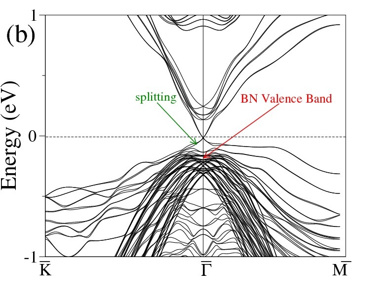
Computed band structures of Bi2Se2Te/BN supercell are seen in Fig. 13. Both asymmetric capping, in Fig. 13(a) (B on the top of Se on one side and vacuum on the other side) and Fig. 13(b) (B on the top of Se on one side and N on the top of Se on the other side), and symmetric capping in Fig. 13(c) (B on the top of Se on both sides) indicate that the Dirac point and the surface state dispersion are preserved. However, small splitting between top and bottom surface bands occurs in the asymmetric case, which are induced by different environments on opposite surfaces, while no such splitting exists in the symmetric structure. The valence band maximum is about 0.25 eV below for all three cases as we can estimate from the band structure of only BN slab in the inset of Fig. 13(a) and atom-projected DOS plots (figures not shown). The bulk band gap sizes (around 0.251 eV) in all BN cappings for Bi2Se2Te increases a little bit as compared with the bulk gap (0.204 eV) of only 4QLs Bi2Se2Te.
Fig. 14 shows band structures of Bi2Te2Se/BN supercell. In Fig. 14(a), the asymmetric capping of B on the top of Te on one side and vacuum on the other side, the fourfold degeneracy at the Dirac point is maintained, but two opposite surface bands seem to split. Another asymmetric capping that Te is on the top of B on one side and N on the other side leads to the split of fourfoud degeneracy into two twofold degeneracies at the -point. The twofold degeneracy on each surface band still remains due to Kramer’s theorem which requires that the twofold degeneracy at the time-reversal invariant momenta points is protected in the absence of time-reversal symmetry breaking perturbations. On the other hands, in the symmetric structure of B on the top of Te on both sides, surface bands on both sides are perfectly aligned as seen in Fig. 14(c). In BN cappings of Bi2Te2Se, the bulk band gap sizes (around 0.33 eV) are a bit larger than 0.325 eV the bulk band gap of 4QLs Bi2Te2Se without BN.
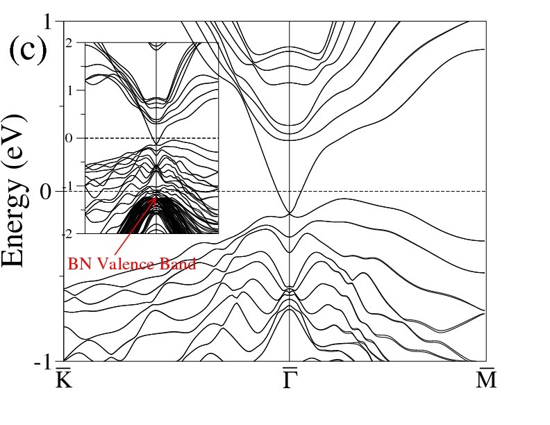
For the capping Bi2Te2Se with the oxygen-terminated quartz without dangling bond passivation, the Dirac cone surface states are highly influenced by the oxygen dangling bond states in Fig. 15(a). From the DOS plot in Fig. 15(b), Bi, Te and Se orbitals are overlapped with oxygen orbitals near the Dirac point. The Dirac point indicated in the inset in Fig. 15(b) is within the valence bands of quartz. The DOS values for Bi, Se and Te at the Dirac point are not zero as shown in the inset because the Dirac point is already buried under the bulk valence band maximum of Bi2Te2Sejiwon . Similarly with Bi2Se3, oxygen dangling states modify Dirac cone surface states without breaking the Dirac point.
IV Summary and Conclusions
We use a density functional based electronic structure method and atom-projected DOS to study the perturbations from dielectric cappings to the Dirac cone surface states of Bi-based binary and ternary TIs. Two crystalline dielectrics BN and quartz were considered with both symmetric and asymmetric cappings. Our study suggests that oxygen coverage substantially affects the Dirac cone, consistent with a recent experimental study. All other surface dielectric terminations have no significant effect on the TI surface states.
Acknowledgements.
The authors acknowledge financial support from the Nanoelectronics Research Initiative supported Southwest Academy of Nanoelectronics (NRI-SWAN) center. We thank Texas advanced computing center (TACC) for computational support (TG-DMR080016N).References
- (1) X.-L. Qi and S.-C. Zhang, Physics Today 63, 33 (2010).
- (2) M. Z. Hasan and C. L. Kane, Rev. Mod. Phys. 82, 3045 (2010).
- (3) B. Yan, H. -J. Zhang, C. -X. Liu, X. -L. Qi, T. Frauenheim, S. -C. Zhang, Phys. Rev. B 82, 161108 (2010).
- (4) D. Xiao, Y. Yao, W. Feng, J. Wen, W. Zhu, X. Q. Chen, G. M. Stocks, Z. Zhang, Phys. Rev. Lett. 105, 096404 (2010).
- (5) W. Feng, D. Xiao, J. Ding, Y. Yao, Phys. Rev. Lett. 106, 016402 (2011).
- (6) S. Chadov, X.-L. Qi, J Kübler, G. H. Fecher, C. Felser, S.-C. Zhang, Nature Mater. 9, 541 (2010).
- (7) H. Lin, L.A. Wray, Y. Xia, S. Jia, R.J. Cava, A. Bansil, M.Z. Hasan, Nature Materials (2010).
- (8) H. Zhang, C. -X. Liu, X. -L. Qi, X. Dai, Z. Fang and S.-C. Zhang, Nature Physics 5, 438 (2009).
- (9) A.A. Burkov, D.G. Hawthorn,PRL 105, 066802 (2010).
- (10) Y. S. Hor, P. Roushan, H. Beidenkopf, J. Seo, D. Qu, J. G. Checkelsky, L. A. Wray, D. Hsieh, Y. Xia, S.-Y. Xu, D. Qian, M. Z. Hasan, N. P. Ong, A. Yazdani, R. J. Cava, Phys. Rev. B 81, 195203 (2010).
- (11) J. P. Perdew, K. Burke and M. Ernzerhof, Phys. Rev. Lett. 77, 3865 (1996).
- (12) C. R. Dean, A. F. Young, I. Meric, C. Lee, L. Wang, S. Sorgenfrei, K. Watanabe, T. Taniguchi, P. Kim, K. L. Shepard and J. Hone, Nat. Nanotech. 5, 722 (2010).
- (13) J. Xue, J. S- Yamagishi, D. Bulmash, P. Jacquod, A. Deshpande, K. Watanabe, T. Taniguchi, P. J- Herrero and B. J. LeRoy, Nat. Mater. 10, 282 (2010).
- (14) D. Kong, J. J. Cha, K. Lai, H. Peng, J. G. Analytis, S. Meister, Y. Chen, H-J Zhang, I. R. Fisher, Z-X Shen, and Y. Cui, ACS Nano 5 (6), 4698-4703 (2011).
- (15) T. Ozaki and H. Kino, Phys. Rev. B 72, 045121 (2005).
- (16) T. Ozaki, Phys. Rev. B 67, 155108 (2003).
- (17) C. -X. Liu, X.-L. Qi, H. J. Zhang, X. Dai, Z. Fang, and S. -C. Zhang, Phys. Rev. B 82, 045122 (2010).
- (18) Y. Zhang, K. He, C. Z. Chang, C. L. Song, L. L. Wang, X. Chen, J. F. Jia, Z. Fang, X. Dai, W. Y. Shan, S. Q. Shen, Q. Niu, X. l. Qi, S. C. Zhang, X. C. Ma and Q. K. Xue, Nature Physics. 6. 584 (2010).
- (19) J. Chang, L. F. Register, S. K. Banerjee and B. Sahu Phys. Rev. B 83, 235108 (2011).
- (20) http://cst-www.nrl.navy.mil/lattice/struk/bk.html.
- (21) K. Watanabe, T. Taniguchi, and H. Kanda, Nat. Mater. 3, 404 (2004).
- (22) http://cst-www.nrl.navy.mil/lattice/struk/sio2a.html.
- (23) E. P. O’Reilly and J. Robertson, Phys. Rev. B 27, 3780 (1983͒).